US7911759B2 - Methods and arrangement for protecting against electrostatic discharge - Google Patents
Methods and arrangement for protecting against electrostatic discharge Download PDFInfo
- Publication number
- US7911759B2 US7911759B2 US12/189,188 US18918808A US7911759B2 US 7911759 B2 US7911759 B2 US 7911759B2 US 18918808 A US18918808 A US 18918808A US 7911759 B2 US7911759 B2 US 7911759B2
- Authority
- US
- United States
- Prior art keywords
- esd
- electronic device
- shield
- shielding
- external cover
- Prior art date
- Legal status (The legal status is an assumption and is not a legal conclusion. Google has not performed a legal analysis and makes no representation as to the accuracy of the status listed.)
- Expired - Fee Related, expires
Links
Images


Classifications
-
- H—ELECTRICITY
- H05—ELECTRIC TECHNIQUES NOT OTHERWISE PROVIDED FOR
- H05K—PRINTED CIRCUITS; CASINGS OR CONSTRUCTIONAL DETAILS OF ELECTRIC APPARATUS; MANUFACTURE OF ASSEMBLAGES OF ELECTRICAL COMPONENTS
- H05K9/00—Screening of apparatus or components against electric or magnetic fields
- H05K9/0067—Devices for protecting against damage from electrostatic discharge
-
- H—ELECTRICITY
- H04—ELECTRIC COMMUNICATION TECHNIQUE
- H04M—TELEPHONIC COMMUNICATION
- H04M1/00—Substation equipment, e.g. for use by subscribers
- H04M1/02—Constructional features of telephone sets
- H04M1/0202—Portable telephone sets, e.g. cordless phones, mobile phones or bar type handsets
-
- Y—GENERAL TAGGING OF NEW TECHNOLOGICAL DEVELOPMENTS; GENERAL TAGGING OF CROSS-SECTIONAL TECHNOLOGIES SPANNING OVER SEVERAL SECTIONS OF THE IPC; TECHNICAL SUBJECTS COVERED BY FORMER USPC CROSS-REFERENCE ART COLLECTIONS [XRACs] AND DIGESTS
- Y10—TECHNICAL SUBJECTS COVERED BY FORMER USPC
- Y10T—TECHNICAL SUBJECTS COVERED BY FORMER US CLASSIFICATION
- Y10T29/00—Metal working
- Y10T29/53—Means to assemble or disassemble
- Y10T29/5313—Means to assemble electrical device
Definitions
- the invention relates to Electrostatic Discharge (ESD) protection in electronic devices and techniques for implementing the same.
- GPS Global Positioning System
- Electronic devices and more particularly portable electronic devices, are ubiquitous these days.
- a typical consumer may carry at times an electronic key fob for opening/closing automobile doors, a cellular phone for communication, a portable music/video player for entertainment, etc.
- electrostatic discharge refers to static electricity discharge that can occur when the electronic device is exposed to a nearby object having a higher electrical potential (i.e., the ESD source).
- ESD electrostatic discharge
- the discharge current path (of which the spark is a part) may traverse one or more sensitive circuits in the electronic device, causing a temporary or permanent malfunction.
- an ESD shield is a conductive shield that presents to the ESD source a lower resistance path to ground. The discharge current that emanates from the ESD source is then diverted onto the ESD shield, thereby preventing the discharge current from causing damage to the sensitive electronic components.
- a conductive or insulative housing or cover that acts as an environmental enclosure and also provides a pleasing cosmetic appearance.
- a typical cellular phone may be encased in a plastic or aluminum housing that provides a mounting framework for the electronic components therein as well as protects the electronic components from environmental damage.
- ESD current typically cannot penetrate the conductive or insulative housing material. Instead, ESD current penetrates the electronic device through joints or interfaces where the housing parts are assembled together. In an example cellular phone, there may be two half shells that form the housing. The joint between these two shells are often vulnerable to ESD current penetration and is often the focus for ESD protection. If one of the shells has other openings, such as an opening to accommodate a battery or a LCD (Liquid Crystal Display) sub-assembly, the opening edges are also vulnerable to ESD current penetration.
- LCD Liquid Crystal Display
- ESD protection is to provide an ESD shield at any location where ESD current penetration may occur.
- this approach also increases the mass and thickness of the resultant electronic device.
- engineers are constantly looking for ways to maintain or improve ESD protection while eliminating bulk and materials from the finished product.
- the finished product has to be aesthetically pleasing.
- ESD protection schemes must therefore also take aesthetic into consideration. Improving ESD protection while minimizing bulk and maintaining a pleasing aesthetic appearance is a subject of the present invention.
- the invention relates, in an embodiment, to an electronic device having ESD (Electrostatic Discharge) protection for a plurality of sides of the electronic device.
- the electronic device includes an external cover configured to externally cover a first side of the electronic device, the external cover having at least one aperture and a plurality of slots disposed sufficiently close to a periphery of the at least one aperture such that ESD current is diverted to material disposed in at least one of the plurality of slots if the ESD current penetrates a gap that exists at the at least one aperture.
- the electronic device further includes an ESD shield configured for providing ESD protection for a second side of an electronic device and also for the first side, the second side being opposite the first side.
- the ESD shield includes an ESD-shielding surface configured to provide the ESD protection for at least a portion of the second side, and a plurality of orthogonally protruding ESD shielding tabs, individual ones of the plurality of orthogonally protruding ESD shielding tabs configured to fit within respective ones of the plurality of slots when the ESD shield is mated with the external cover.
- FIGS. 1A , 1 B and 1 C show a flip-out cellular phone
- FIG. 2 shows, in accordance with one or more embodiments of the present invention, an ESD shield 200 having an ESD-shielding surface 202 and integrated ESD shielding walls and/or tabs.
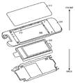
- FIG. 3 shows, in accordance with one or more embodiments of the present invention, an exploded view of the LCD-containing subsystem of an example flip-out cellular phone, including the inventive ESD shield.
- FIG. 4 shows, in accordance with one or more embodiments of the present invention, an enlarged view of a slot 402 configured to accommodate one of the ESD-shielding tabs.
- the invention might also cover articles of manufacture that includes a computer readable medium on which computer-readable instructions for carrying out embodiments of the inventive technique are stored.
- the computer readable medium may include, for example, semiconductor, magnetic, opto-magnetic, optical, or other forms of computer readable medium for storing computer readable code.
- the invention may also cover apparatuses for practicing embodiments of the invention. Such apparatus may include circuits, dedicated and/or programmable, to carry out tasks pertaining to embodiments of the invention. Examples of such apparatus include a general-purpose computer and/or a dedicated computing device when appropriately programmed and may include a combination of a computer/computing device and dedicated/programmable circuits adapted for the various tasks pertaining to embodiments of the invention.
- Embodiments of the invention relate to an ESD protection arrangement for protecting multiple sides of a given electronic device.
- an electrically conductive frame having an ESD-shielding surface and integrated but orthogonally protruding ESD-shielding walls and/or tabs is provided to provide ESD protection.
- the ESD-shielding surface is configured to protect ESD-sensitive devices that are disposed behind the ESD-shielding surface.
- the orthogonally protruding ESD-shielding walls and/or tabs are configured to extend ESD protection to one or more other sides of the device.
- a cellular phone may be formed of two main portions.
- the two main portions may be housed in two separate housings that are pivotally connected with one another.
- Such a cellular phone design may be referred to commonly as a clam-shell or slide-out or flip-out design, wherein one part of the cellular phone may house a portion of the circuitry and/or the keypad and the other part may house the display(s).
- the invention is not limited to clam-shell cellular phones or the display-containing portion of the cellular phone, the display-containing portion, and particularly a display-containing portion having at least two LCD panels, will be used to facilitate discussion of relevant details of the invention.
- the display-containing portion may include a housing having a plurality of apertures to allow the user to view one or more displays.
- An ESD shield may be provided wherein the ESD-shielding surface is configured to protect one side of the display-containing portion and the orthogonally protruding ESD-shielding walls and/or tabs may be configured to protect the edges as well as the opposite side.
- a single ESD shield may protect two or more sides of the electronic device while requiring minimal additional bulk or adding minimal, if any, additional thickness to the finished product.
- the orthogonally protruding ESD-shielding tabs may be hidden in slots in the housing in order preserve the aesthetically pleasing look of the finished product.
- FIGS. 1A , 1 B and 1 C show a flip-out cellular phone 102 having a first portion 104 and a second portion 106 , both of which are enclosed in their own housings and are pivotally connected with one another.
- First portion 104 represents the display-containing portion and includes a housing 120 having two apertures for accommodating two LCDs 108 ( FIG. 1C) and 110 ( FIG. 1B ).
- LCD 108 is intended to be viewed from the front side of housing 120
- LCD 110 is intended to be viewed from opposite side (backside) of housing 120 .
- These two LCDs are shown in the front view and back view of first portion 104 in FIG. 1C and FIG. 1B respectively.
- apertures are provided in opposite sides of housing 120 to accommodate LCDs 108 and 110 .
- housing 120 is formed of a conductive or insulative material (such as aluminum or plastic). If housing 120 is a metallic housing, and a path to ground is not already provided with housing 120 , the inventive ESD protection arrangement is particularly useful. ESD current tends not to be able to penetrate the housing material, thus rendering electronic devices housed therein relatively safe from ESD-related damage. Likewise, ESD current tends to not be able to penetrate the material that forms the LCD lens (such as transparent polycarbonate material). Accordingly, electronic components protected by the LCD lens are also relatively safe from ESD-related damage.
- Areas vulnerable to ESD-related damage include the edge of the apertures formed in housing 120 to accommodate LCDs 108 and 110 . If these edges ( 144 and 146 ) are inadequately protected, ESD current may be able to reach sensitive electronic components within display-containing portion 104 , rendering those sensitive electronic components temporarily or permanently damaged. If housing 120 is formed of multiple pieces that snap or are fastened together, similar vulnerability exists with respect to the joints where the housing pieces mate together.
- FIG. 2 shows, in accordance with one or more embodiments of the present invention, an ESD shield 200 having an ESD-shielding surface 202 and integrated ESD shielding walls and/or tabs.
- ESD shield 200 may be formed of a conductive material, such as metal or metallized plastic, in order to present a low resistance path to ground for the purpose of providing ESD protection.
- ESD shield 200 has an aperture 204 , the edge of which is configured to surround a LCD panel that projects light/text/images in the direction into the page of FIG. 2 (front to back direction in FIG. 2 ).
- the edge 206 of aperture 204 being in close proximity to the edge of the LCD panel, presents a low resistance path to ground to divert damaging ESD current from penetrating into the device through the gap between the LCD panel edge and edge 206 of ESD shield 200 .
- ESD shield 200 also functions as a back portion of the housing to enclose circuit 302 .
- the other portion of the housing is shown in FIG. 3 as front cover 304 , which may be formed of a material (such as a metal or plastic) that can provide both environmental and ESD protection to circuit 302 .
- Front cover 304 is configured as an external cover to cover the front side of the electronic device, in one or more embodiments.
- ESD shield 200 may include, in an embodiment, raised walls 210 a and 210 b , which protrude orthogonally from ESD shielding surface 202 .
- Walls 210 a and 210 b provide ESD protection for the edge of the device by presenting a low resistance path to ground, thereby preventing ESD current from being able to penetrate into the electronic device through the side of the device.
- Walls 210 a and 210 b may be extended to wrap around most or all of the periphery of ESD shield 200 to provide ESD protection from all around the edge.
- Walls 210 a and 210 b may be varied in height at various locations to accommodate different designs, if desired.
- Front cover 304 has an aperture 306 for accommodating a LCD display (front of circuit 302 ) to allow the LCD display to project light text image toward the front of the device.
- a LCD lens 310 covers the LCD panel and provides environmental as well as ESD protection for the LCD panel circuitry. Since the ESD current cannot penetrate the material of front cover 304 or the material of the LCD lens (which may be made of, for example, polycarbonate), the edge 312 where LCD lens 310 meets with the edge of aperture 306 represents one of the remaining areas vulnerable to ESC current penetration.
- ESD-shielding tabs which are orthogonal to ESD-shielding surface 202 , are provided with ESD shield 200 to facilitate insertion into slots built into front cover 304 of the device housing.
- ESD shielding tabs Four of these ESD shielding tabs may be seen as tabs 212 a , 212 b , 212 c , and 212 d .
- 8 ESD shielding tabs 8 ESD shielding tabs are shown, the number of ESD shielding tabs may vary as desired.
- the dimension of each ESD-shielding tab may also be varied as desired and all ESD-shielding tabs may have the same size and height or different ESD-shielding tabs may have different sizes and/or different heights.
- FIG. 4 shows, in accordance with one or more embodiments, an enlarged view of a slot 402 configured to accommodate one of the ESD-shielding tabs.
- slot 402 (and one or more other slots) is/are disclosed sufficiently close to a periphery of the aperture formed in front cover 304 such that ESD current is diverted to the tab disposed in slot 402 (or one or more other slots) if the ESD current attempts to penetrate the front cover gap around the aperture.
- ESD current is diverted to the tab disposed in slot 402 (or one or more other slots) if the ESD current attempts to penetrate the front cover gap around the aperture.
- the ESD-shielding tab may rest slightly protruded out of slot 402 after front cover 304 and ESD shield 200 are mated together. In an embodiment the ESD-shielding tab may rest flushed with slot 402 after front cover 304 and ESD shield 200 are mated together. In an embodiment, the ESD-shielding tab may rest slightly recessed with respect to slot 402 after front cover 304 and ESD shield 200 are mated together. Front cover 304 typically has sufficient slots to accommodate all ESD-shielding tabs.
- slot 402 is slightly inward of the outside edge of the electronic device.
- slot 402 is formed on an internal shelf 430 that is invisible from outside the finished device when looking at the device from the edge. In this manner, when front cover 304 and ESD shield 200 are mated together, the ESD-shielding tabs may be invisible from the edge since they are inserted into their slots and only walls 210 a and 210 b may be visible from the edge of the device.
- Internal shelf 430 represents a shelf also for supporting LCD lens 310 to allow the LCD and the LCD lens 310 to achieve a more flushed appearance with respect to front cover 304 when LCD lens 310 is fitted into the aperture of front cover 304 .
- Internal shelf 430 is supported by a wall 432 , which may also provide some degree of mechanical support and alignment for walls 210 a and 210 b of ESD shield 200 when front cover 304 and ESD shield 200 are mated together.
- a downwardly extending partial wall or lip may be provided with front cover 304 to overlap and visually cover the joint between wall 210 a / 210 b and front cover 304 if desired. Material left in between adjacent slots provides mechanical strength to internal shelf 430 and front cover 304 as a whole.
- LCD lens 310 covers the slots (and the ESD-shielding tabs in the slots) when LCD lens 310 is disposed on inner shelf 430 in the finished product.
- the presence of the ESD-shielding material (such as metal or a metallized plastic of the ESD shield) of the tab in slot 402 presents a low resistance path to ground for any ESD current attempting to penetrate the gap between front cover 304 and LCD lens 310 .
- Any ESD current attempting to penetrate the gap between front cover 304 and LCD lens 310 would be diverted to one of the ESD shielding tabs and harmless conducted to ground.
- the materials of front cover 304 and LCD lens 310 already provide ESD protection for most of the front side of the electronic device.
- the ESD-shielding tabs which are integrally formed with the ESD shield that protects the backside and the edge of the device, the remaining vulnerable area of the front side of the device (e.g., the gap between front cover 304 and LCD lens 310 ) is also protected.
- the innovative ESD shielding arrangement provides protection for the back side, the edge, and the front side of the electronic device with a single ESD shield.
- the thickness of the device is not adversely affected since the slots are formed on an internal shelf that already exists to support the LCD lens.
- the ESD-shielding tabs are hidden from view from the side after assembly (by being hidden in the slots) and also invisible from the top after assembly (by being covered with the LCD lens). Accordingly, improved ESD protection is achieved without incurring significant penalty in device thickness or in aesthetic.
- a portion of the ESD shield may be formed of a non-conductive material as long as the ESD shielding tabs are formed of a conductive material and there is a path from the ESD shielding tabs to ground for diverting ESD current.
- the discussion employs a portion of a cellular phone to facilitate discussion, the ESD shielding arrangement and technique may be applicable to any portion or the whole of any electronic device, irrespective whether the electronic device is intended to be stationary or portable, when ESD protection from multiple sides is desired.
- a portion of the ESD shield may be formed of a non-conductive material as long as the ESD shielding tabs are formed of a conductive material, and there is a path from the ESD shielding tabs to ground for diverting ESD current.
- the discussion employs a portion of a cellular phone to facilitate discussion
- the ESD shielding arrangement and technique may be applicable to any portion or the whole of any electronic device, irrespective whether the electronic device is intended to be stationary or portable, when ESD protection from multiple sides is desired.
Landscapes
- Engineering & Computer Science (AREA)
- Signal Processing (AREA)
- Microelectronics & Electronic Packaging (AREA)
- Telephone Set Structure (AREA)
- Devices For Indicating Variable Information By Combining Individual Elements (AREA)
- Shielding Devices Or Components To Electric Or Magnetic Fields (AREA)
Abstract
Description
Claims (20)
Priority Applications (4)
| Application Number | Priority Date | Filing Date | Title |
|---|---|---|---|
| US12/189,188 US7911759B2 (en) | 2008-08-10 | 2008-08-10 | Methods and arrangement for protecting against electrostatic discharge |
| CN2009801310939A CN102172110A (en) | 2008-08-10 | 2009-08-10 | Methods and settings for protection against electrostatic discharge |
| JP2011522305A JP2011530900A (en) | 2008-08-10 | 2009-08-10 | Method and configuration for protecting against electrostatic discharge |
| PCT/US2009/053280 WO2010019502A1 (en) | 2008-08-10 | 2009-08-10 | Methods and arrangement for protecting against electrostatic discharge |
Applications Claiming Priority (1)
| Application Number | Priority Date | Filing Date | Title |
|---|---|---|---|
| US12/189,188 US7911759B2 (en) | 2008-08-10 | 2008-08-10 | Methods and arrangement for protecting against electrostatic discharge |
Publications (2)
| Publication Number | Publication Date |
|---|---|
| US20100033886A1 US20100033886A1 (en) | 2010-02-11 |
| US7911759B2 true US7911759B2 (en) | 2011-03-22 |
Family
ID=41131651
Family Applications (1)
| Application Number | Title | Priority Date | Filing Date |
|---|---|---|---|
| US12/189,188 Expired - Fee Related US7911759B2 (en) | 2008-08-10 | 2008-08-10 | Methods and arrangement for protecting against electrostatic discharge |
Country Status (4)
| Country | Link |
|---|---|
| US (1) | US7911759B2 (en) |
| JP (1) | JP2011530900A (en) |
| CN (1) | CN102172110A (en) |
| WO (1) | WO2010019502A1 (en) |
Cited By (2)
| Publication number | Priority date | Publication date | Assignee | Title |
|---|---|---|---|---|
| US9690407B2 (en) * | 2014-08-19 | 2017-06-27 | Htc Corporation | Electronic device cover plate for draining electrostatic charges using conductive layer connection to ground and electronic device having the same |
| US10524370B2 (en) | 2017-06-28 | 2019-12-31 | Seagate Technology Llc | Electrostatic charge build-up prevention for data storage devices |
Families Citing this family (3)
| Publication number | Priority date | Publication date | Assignee | Title |
|---|---|---|---|---|
| JP5451149B2 (en) * | 2009-04-08 | 2014-03-26 | キヤノン株式会社 | Electronics |
| WO2013118164A1 (en) * | 2012-02-06 | 2013-08-15 | パナソニック株式会社 | Mobile terminal device |
| CN111867343B (en) * | 2019-04-30 | 2023-08-04 | 北京小米移动软件有限公司 | Terminal equipment and protective housing |
Citations (4)
| Publication number | Priority date | Publication date | Assignee | Title |
|---|---|---|---|---|
| US6483719B1 (en) * | 2000-03-21 | 2002-11-19 | Spraylat Corporation | Conforming shielded form for electronic component assemblies |
| US6728555B1 (en) * | 1999-09-29 | 2004-04-27 | Nokia Mobile Phones, Ltd. | Display frame with integrated ESD shield, and a user interface construction |
| US20060055841A1 (en) | 2004-09-10 | 2006-03-16 | Petri Keski-Opas | ESD protection for LCD panels and the like |
| DE102006040525B3 (en) | 2006-08-30 | 2008-04-30 | Johnson Controls Automotive Electronics Gmbh | Potential limiter for electronic device e.g. liquid crystal display, has electrically conductive connection to reference potential and circuit medium e.g. copper strip, for connection at electronic device |
Family Cites Families (2)
| Publication number | Priority date | Publication date | Assignee | Title |
|---|---|---|---|---|
| SE505004C2 (en) * | 1996-01-18 | 1997-06-09 | Ericsson Telefon Ab L M | Protective device for electromagnetic coupling and electrostatic discharge and use thereof |
| JP2006135842A (en) * | 2004-11-09 | 2006-05-25 | Mitsubishi Electric Corp | Portable electronic devices |
-
2008
- 2008-08-10 US US12/189,188 patent/US7911759B2/en not_active Expired - Fee Related
-
2009
- 2009-08-10 WO PCT/US2009/053280 patent/WO2010019502A1/en not_active Ceased
- 2009-08-10 JP JP2011522305A patent/JP2011530900A/en active Pending
- 2009-08-10 CN CN2009801310939A patent/CN102172110A/en active Pending
Patent Citations (4)
| Publication number | Priority date | Publication date | Assignee | Title |
|---|---|---|---|---|
| US6728555B1 (en) * | 1999-09-29 | 2004-04-27 | Nokia Mobile Phones, Ltd. | Display frame with integrated ESD shield, and a user interface construction |
| US6483719B1 (en) * | 2000-03-21 | 2002-11-19 | Spraylat Corporation | Conforming shielded form for electronic component assemblies |
| US20060055841A1 (en) | 2004-09-10 | 2006-03-16 | Petri Keski-Opas | ESD protection for LCD panels and the like |
| DE102006040525B3 (en) | 2006-08-30 | 2008-04-30 | Johnson Controls Automotive Electronics Gmbh | Potential limiter for electronic device e.g. liquid crystal display, has electrically conductive connection to reference potential and circuit medium e.g. copper strip, for connection at electronic device |
Cited By (2)
| Publication number | Priority date | Publication date | Assignee | Title |
|---|---|---|---|---|
| US9690407B2 (en) * | 2014-08-19 | 2017-06-27 | Htc Corporation | Electronic device cover plate for draining electrostatic charges using conductive layer connection to ground and electronic device having the same |
| US10524370B2 (en) | 2017-06-28 | 2019-12-31 | Seagate Technology Llc | Electrostatic charge build-up prevention for data storage devices |
Also Published As
| Publication number | Publication date |
|---|---|
| CN102172110A (en) | 2011-08-31 |
| US20100033886A1 (en) | 2010-02-11 |
| JP2011530900A (en) | 2011-12-22 |
| WO2010019502A1 (en) | 2010-02-18 |
Similar Documents
| Publication | Publication Date | Title |
|---|---|---|
| US7911759B2 (en) | Methods and arrangement for protecting against electrostatic discharge | |
| US8520373B2 (en) | Display assembly for a portable module | |
| US8482697B2 (en) | Protecting module and portable electronic device using the same | |
| KR101537438B1 (en) | A housing for a portable electronic device | |
| EP2773083B1 (en) | Fixation of the battery with a metal plate to the housing of an electronic device | |
| US7957123B2 (en) | Portable electronic device | |
| US20130330951A1 (en) | Connector of electronic device, plug of electronic device, and waterproof structure of electronic device | |
| EP3509278B1 (en) | Electronic component and electronic device comprising same | |
| US8444439B2 (en) | Connector mounting apparatus having a bracket with recesses abutting resisting tabs of a member received therein | |
| AU2011203352B1 (en) | Silicon case | |
| JP2009194223A (en) | Mobile terminal device and method of grounding mobile terminal device | |
| KR101413491B1 (en) | Door for Protection against Electromagnetic Wave and Radioactivity | |
| US10021228B2 (en) | Cradle with privacy protection function for portable electronic device | |
| US20090296976A1 (en) | Electronic device having a receiver | |
| JP2012114663A (en) | Electronic apparatus | |
| US10387708B2 (en) | Physiological characteristic identifying module | |
| CN104811590A (en) | Portable electronic device and camera module set thereof | |
| US8254099B2 (en) | Housing of portable electronic device | |
| US20160034003A1 (en) | Electronic device | |
| JP4889781B2 (en) | Mobile terminal device | |
| TWI344028B (en) | Display apparatus with electrostatic discharge protection | |
| US7778676B2 (en) | ESD protection for LCD panels and the like | |
| CN220173297U (en) | Prevent sheltering from camera lens support protective housing | |
| CN111356313A (en) | Housing assembly and electronic device | |
| KR100539806B1 (en) | Handheld terminal |
Legal Events
| Date | Code | Title | Description |
|---|---|---|---|
| AS | Assignment |
Owner name: KYOCERA WIRELESS CORP.,CALIFORNIA Free format text: ASSIGNMENT OF ASSIGNORS INTEREST;ASSIGNORS:WILLIAMS, GREGORY L.;CHOI, KWANGHYUN DAVID;SIGNING DATES FROM 20080709 TO 20080730;REEL/FRAME:021369/0791 Owner name: KYOCERA WIRELESS CORP., CALIFORNIA Free format text: ASSIGNMENT OF ASSIGNORS INTEREST;ASSIGNORS:WILLIAMS, GREGORY L.;CHOI, KWANGHYUN DAVID;SIGNING DATES FROM 20080709 TO 20080730;REEL/FRAME:021369/0791 |
|
| AS | Assignment |
Owner name: KYOCERA CORPORATION,JAPAN Free format text: ASSIGNMENT OF ASSIGNORS INTEREST;ASSIGNOR:KYOCERA WIRELESS CORP.;REEL/FRAME:024170/0005 Effective date: 20100326 Owner name: KYOCERA CORPORATION, JAPAN Free format text: ASSIGNMENT OF ASSIGNORS INTEREST;ASSIGNOR:KYOCERA WIRELESS CORP.;REEL/FRAME:024170/0005 Effective date: 20100326 |
|
| STCF | Information on status: patent grant |
Free format text: PATENTED CASE |
|
| FPAY | Fee payment |
Year of fee payment: 4 |
|
| FEPP | Fee payment procedure |
Free format text: MAINTENANCE FEE REMINDER MAILED (ORIGINAL EVENT CODE: REM.); ENTITY STATUS OF PATENT OWNER: LARGE ENTITY |
|
| LAPS | Lapse for failure to pay maintenance fees |
Free format text: PATENT EXPIRED FOR FAILURE TO PAY MAINTENANCE FEES (ORIGINAL EVENT CODE: EXP.); ENTITY STATUS OF PATENT OWNER: LARGE ENTITY |
|
| STCH | Information on status: patent discontinuation |
Free format text: PATENT EXPIRED DUE TO NONPAYMENT OF MAINTENANCE FEES UNDER 37 CFR 1.362 |
|
| FP | Lapsed due to failure to pay maintenance fee |
Effective date: 20190322 |