US7892900B2 - Integrated circuit system employing sacrificial spacers - Google Patents
Integrated circuit system employing sacrificial spacers Download PDFInfo
- Publication number
- US7892900B2 US7892900B2 US12/098,751 US9875108A US7892900B2 US 7892900 B2 US7892900 B2 US 7892900B2 US 9875108 A US9875108 A US 9875108A US 7892900 B2 US7892900 B2 US 7892900B2
- Authority
- US
- United States
- Prior art keywords
- spacer
- dielectric layer
- forming
- integrated circuit
- circuit system
- Prior art date
- Legal status (The legal status is an assumption and is not a legal conclusion. Google has not performed a legal analysis and makes no representation as to the accuracy of the status listed.)
- Active, expires
Links
Images


Classifications
-
- H—ELECTRICITY
- H10—SEMICONDUCTOR DEVICES; ELECTRIC SOLID-STATE DEVICES NOT OTHERWISE PROVIDED FOR
- H10D—INORGANIC ELECTRIC SEMICONDUCTOR DEVICES
- H10D30/00—Field-effect transistors [FET]
- H10D30/60—Insulated-gate field-effect transistors [IGFET]
- H10D30/791—Arrangements for exerting mechanical stress on the crystal lattice of the channel regions
- H10D30/792—Arrangements for exerting mechanical stress on the crystal lattice of the channel regions comprising applied insulating layers, e.g. stress liners
-
- H—ELECTRICITY
- H10—SEMICONDUCTOR DEVICES; ELECTRIC SOLID-STATE DEVICES NOT OTHERWISE PROVIDED FOR
- H10D—INORGANIC ELECTRIC SEMICONDUCTOR DEVICES
- H10D84/00—Integrated devices formed in or on semiconductor substrates that comprise only semiconducting layers, e.g. on Si wafers or on GaAs-on-Si wafers
- H10D84/01—Manufacture or treatment
- H10D84/0123—Integrating together multiple components covered by H10D12/00 or H10D30/00, e.g. integrating multiple IGBTs
- H10D84/0126—Integrating together multiple components covered by H10D12/00 or H10D30/00, e.g. integrating multiple IGBTs the components including insulated gates, e.g. IGFETs
- H10D84/0165—Integrating together multiple components covered by H10D12/00 or H10D30/00, e.g. integrating multiple IGBTs the components including insulated gates, e.g. IGFETs the components including complementary IGFETs, e.g. CMOS devices
- H10D84/0167—Manufacturing their channels
-
- H—ELECTRICITY
- H10—SEMICONDUCTOR DEVICES; ELECTRIC SOLID-STATE DEVICES NOT OTHERWISE PROVIDED FOR
- H10D—INORGANIC ELECTRIC SEMICONDUCTOR DEVICES
- H10D84/00—Integrated devices formed in or on semiconductor substrates that comprise only semiconducting layers, e.g. on Si wafers or on GaAs-on-Si wafers
- H10D84/01—Manufacture or treatment
- H10D84/0123—Integrating together multiple components covered by H10D12/00 or H10D30/00, e.g. integrating multiple IGBTs
- H10D84/0126—Integrating together multiple components covered by H10D12/00 or H10D30/00, e.g. integrating multiple IGBTs the components including insulated gates, e.g. IGFETs
- H10D84/0165—Integrating together multiple components covered by H10D12/00 or H10D30/00, e.g. integrating multiple IGBTs the components including insulated gates, e.g. IGFETs the components including complementary IGFETs, e.g. CMOS devices
- H10D84/0184—Manufacturing their gate sidewall spacers
-
- H—ELECTRICITY
- H10—SEMICONDUCTOR DEVICES; ELECTRIC SOLID-STATE DEVICES NOT OTHERWISE PROVIDED FOR
- H10D—INORGANIC ELECTRIC SEMICONDUCTOR DEVICES
- H10D84/00—Integrated devices formed in or on semiconductor substrates that comprise only semiconducting layers, e.g. on Si wafers or on GaAs-on-Si wafers
- H10D84/01—Manufacture or treatment
- H10D84/02—Manufacture or treatment characterised by using material-based technologies
- H10D84/03—Manufacture or treatment characterised by using material-based technologies using Group IV technology, e.g. silicon technology or silicon-carbide [SiC] technology
- H10D84/038—Manufacture or treatment characterised by using material-based technologies using Group IV technology, e.g. silicon technology or silicon-carbide [SiC] technology using silicon technology, e.g. SiGe
Definitions
- the present invention relates generally to integrated circuits, and more particularly to an integrated circuit system employing sacrificial spacers.
- Integrated circuits find application in many of today's consumer electronics, such as cell phones, video cameras, portable music players, printers, computers, etc.
- Integrated circuits may include a combination of active devices, passive devices and their interconnections.
- Active devices such as a metal-oxide-semiconductor field-effect transistor (MOSFET) generally include a semiconductor substrate, having a source, a drain, and a channel located between the source and drain.
- a gate stack composed of a conductive material (i.e., a gate) and an oxide layer (i.e., a gate oxide) are typically located directly above the channel.
- an inversion layer forms a conducting bridge or “channel” between the source and drain when a voltage is applied to the gate.
- CMOS complementary-metal-oxide-semiconductor
- the present invention provides an integrated circuit system including: providing a substrate including a first device and a second device; configuring the first device and the second device to include a first spacer, a first liner made from a first dielectric layer, and a second spacer made from a sacrificial spacer material; forming a second dielectric layer over the integrated circuit system; forming a first device source/drain and a second device source/drain adjacent the second spacer and through the second dielectric layer; removing the second spacer without damaging the substrate; forming a third dielectric layer over the integrated circuit system before annealing; and forming a fourth dielectric layer over the integrated circuit system that promotes stress within the channel of the first device, the second device, or a combination thereof.
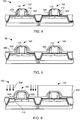
- FIG. 1 is a partial cross sectional view of an integrated circuit system in an initial stage of manufacture in accordance with an embodiment of the present invention
- FIG. 2 is the structure of FIG. 1 after forming a first dielectric layer
- FIG. 3 is the structure of FIG. 2 after forming a sacrificial spacer material
- FIG. 4 is the structure of FIG. 3 after forming a second spacer and a first liner
- FIG. 5 is the structure of FIG. 4 after forming a second dielectric layer
- FIG. 6 is the structure of FIG. 5 during formation of a first device source/drain
- FIG. 7 is the structure of FIG. 6 during formation of a second device source/drain
- FIG. 8 is the structure of FIG. 7 after removal of a second mask layer
- FIG. 9 is the structure of FIG. 8 after removing the second dielectric layer
- FIG. 10 is the structure of FIG. 9 after removing the second spacer
- FIG. 11 is the structure of FIG. 10 after forming a third dielectric layer
- FIG. 12 is the structure of FIG. 11 after forming an electrical contact
- FIG. 13 is the structure of FIG. 12 after further processing
- FIG. 14 is a flow chart of an integrated circuit system for an integrated circuit system in accordance with an embodiment of the present invention.
- horizontal as used herein is defined as a plane parallel to the conventional plane or surface of the substrate, regardless of its orientation.
- vertical refers to a direction perpendicular to the horizontal as just defined. Terms, such as “on”, “above”, “below”, “bottom”, “top”, “side” (as in “sidewall”), “higher”, “lower”, “upper”, “over”, and “under”, are defined with respect to the horizontal plane.
- processing includes deposition of material or photoresist, patterning, exposure, development, implanting, etching, cleaning, and/or removal of the material or photoresist as required in forming a described structure.
- example or “exemplary” are used herein to mean serving as an instance or illustration. Any aspect or embodiment described herein as an “example” or as “exemplary” is not necessarily to be construed as preferred or advantageous over other aspects, embodiments, or designs.
- first”, “second”, “third”, “fourth”, and “fifth” as used herein are for purposes of differentiation between elements only and are not to be construed as limiting the scope of the present invention.
- system means and refers to the method and to the apparatus of the present invention in accordance with the context in which the term is used.
- stress inducing layer includes one or more materials or layers that affects the physical properties, such as carrier mobility, of an adjacent structure or element.
- sacrificial spacer material includes one or more materials or layers that can be removed without causing damage to underlying layers (e.g., no active region silicon loss).
- FIGS. 1-13 depict by way of example and not by limitation, an exemplary process flow for the formation of an integrated circuit system and they are not to be construed as limiting. It is to be understood that a plurality of conventional processes that are well known within the art and not repeated herein, may precede or follow FIGS. 1-13 . Moreover, it is to be understood that many modifications, additions, and/or omissions may be made to the below described process without departing from the scope or spirit of the claimed subject matter. For example, the below described process may include more, fewer, or other steps. Additionally, steps may be performed in any suitable order without departing from the scope of the present invention.
- the integrated circuit system of the present disclosure may include any number of multi-electrode devices in which the current flowing between two specified electrodes is controlled or modulated by the voltage applied at a control electrode.
- Exemplary illustrations may include an n-channel field effect transistor (NFET), a p-channel field effect transistor (PFET), a complementary metal-oxide-silicon (CMOS) configuration, a single-gate transistor, a multi-gate transistor, a fin-FET, or an annular gate transistor.
- NFET n-channel field effect transistor
- PFET p-channel field effect transistor
- CMOS complementary metal-oxide-silicon
- the integrated circuit system of the present disclosure may also include any number of resistance devices with varying resistance values formed by strategically altering the process techniques.
- one or more of the integrated circuit system could be prepared at one time on a medium, which could be separated into individual or multiple integrated circuit assemblies at a later stage of fabrication.
- the following embodiments relate to the formation of an integrated circuit system including, but not limited to, an active device structure with strategically engineered sacrificial spacers whose removal does not damage underlying layers.
- the integrated circuit system 100 may include a first device 102 and a second device 104 .
- the first device 102 and the second device 104 may more particularly include, for example, active devices, such as NFET devices, PFET devices and/or a combination thereof (e.g., a CMOS device structure).
- the first device 102 and the second device 104 may also include one or more passive devices, such as resistors.
- the first device 102 and the second device 104 may include a combination of active and passive devices acting in concert or independently.
- the first device 102 and the second device 104 are not limited to the preceding examples and may include any number of active devices, passive devices, or any combination thereof.
- the integrated circuit system 100 manufactured by the embodiments described herein can be used within a multitude of electronic systems, such as processor components, memory components, logic components, digital components, analog components, mixed-signal components, power components, radio-frequency (RF) components (e.g., RF CMOS circuits), digital signal processor components, micro-electromechanical components, optical sensor components, and so forth, in numerous configurations and arrangements as may be needed.
- RF radio-frequency
- the first device 102 and the second device 104 can be formed over, on and/or within a substrate 106 by conventional deposition, patterning, photolithography, and etching techniques known in the semiconductor processing industry for the manufacture of active devices.
- the substrate 106 may include any semiconducting material, such as, Si, SiC, SiGe, Si/SiGe, SiGeC, Ge, GaAs, InAs, InP, other III/V or II/VI compound semiconductors, as well as silicon-on-insulator configurations.
- the substrate 106 may also include doped and undoped configurations, epitaxial layers, strained configurations, and one or more crystal orientations (e.g., ⁇ 100>, ⁇ 110>, and/or ⁇ 111> orientations), which may be strategically employed to optimize carrier mobility within NFET and/or PFET devices.
- the substrate 106 may also include any material that becomes amorphous upon implantation.
- the substrate 106 may possess a thickness ranging from about one hundred (100) nanometers to about several hundred microns, for example.
- the examples provided for the substrate 106 are not to be construed as limiting and the composition of the substrate 106 may include any surface, material, configuration, or thickness that physically and electrically enables the formation of active and/or passive device structures.
- the first device 102 and the second device 104 both include a well 108 , a gate 110 , a gate dielectric 112 , a channel 114 , a first spacer 116 , a source/drain extension 118 , and a halo region 120 .
- each of the well 108 can be formed within the substrate 106 prior to or subsequent to the formation of the gate 110 and the gate dielectric 112 , depending upon, for example, the desired dopant concentration within the channel 114 .
- the dopants used to form each of the well 108 are of opposite conductivity type as compared to the dopants used to form the source/drain extension 118 , i.e., p-type impurities for NFET devices and n-type impurities for PFET devices.
- the depth, dopant concentration, and energy used to form the well 108 can depend upon the dopant used and the design specifications of the first device 102 and the second device 104 .
- the gate 110 may be formed from conventional materials including doped and undoped semiconducting materials (such as, for example, polySi, amorphous Si, or SiGe), a metal, a metallic alloy, a silicide, or a combination thereof, for example.
- the gate 110 may also include any conducting material or composition that becomes amorphous upon implantation. Regardless of the composition of the gate 110 , the gate 110 may include a critical dimension, i.e., a cross-sectional width, of 45 nanometers or less.
- the gate dielectric 112 may be made from materials including, but not limited to, silicon oxide, silicon oxynitride, silicon nitride, a silicon oxide/nitride/oxide stack, a high-k dielectric material (i.e.—one having a dielectric constant value greater than silicon oxide), or a combination thereof.
- the type of material chosen for the gate dielectric 112 is not limited to the above examples; for example, the gate dielectric 112 may include any material that permits induction of a charge in the channel 114 when an appropriate voltage is applied to the gate 110 . Accordingly, other materials, which may be known to those skilled in the art for gate structures, may also be used for the gate 110 and the gate dielectric 112 .
- the thickness of the gate 110 is between about 500 angstroms and about 3000 angstroms and the thickness of the gate dielectric 112 is between about 10 angstroms and about 50 angstroms. However, larger or smaller thicknesses of the gate 110 and the gate dielectric 112 may be appropriate depending on the design specifications of the first device 102 and the second device 104 .
- the first spacer 116 may be formed from the deposition and anisotropic etching of conventional dielectric materials such as an oxide, a nitride, or a combination thereof. In some embodiments, the first spacer 116 can be formed from the deposition and anisotropic etching of silicon oxide. However, it is to be understood that the type of materials chosen for the first spacer 116 are not limited to the above examples and may include any material that permits electrical isolation of the gate 110 and formation of the source/drain extension 118 aligned to the first spacer 116 . By way of example, the first spacer 116 can be formed by a variety of techniques, including, but not limited to, physical vapor deposition, chemical vapor deposition and thermal oxidation, followed by an appropriate anisotropic etch.
- the thickness and/or width of the first spacer 116 at its interface with the substrate 106 can vary between about 50 angstroms and about 500 angstroms. In a preferred aspect of the embodiment, the thickness and/or width of the first spacer 116 at its interface with the substrate 106 can vary between about 80 angstroms and about 200 angstroms. However, it is to be understood that the thickness of the first spacer 116 can vary with the design specifications of the first device 102 and the second device 104 , such as, but not limited to, critical dimension scaling, placement of the source/drain extension 118 and/or placement of the halo region 120 .
- the thickness of the first spacer 116 may include without limitation any thickness that is optimized to strategically affect the formation of subsequently formed source and drain regions, source and drain contact formations, and/or the proximity of a subsequently deposited stress inducing layer (i.e., a layer that can enhance carrier mobility within the channel region of an active device).
- the first device 102 and the second device 104 may also include the source/drain extension 118 formed adjacent the gate 110 and optionally aligned to the first spacer 116 .
- the source/drain extension 118 may be formed to a shallow depth with a low concentration of impurities relative to a source and drain region.
- the impurities used to form the source/drain extension 118 may include n-type or p-type, depending on the first device 102 and/or the second device 104 being formed (e.g., n-type impurities for an NMOS device and p-type impurities for a PMOS device).
- the impurities used to form the source/drain extension 118 are of the same conductivity type as the impurities used to form a source and drain region. It is to be understood that the source/drain extension 118 can be formed via an angled or perpendicular, with respect to the conventional surface of the substrate 106 , implant that can be aligned to the gate 110 or the first spacer 116 .
- a halo implant can help to decrease the length of the channel 110 , which may be advantageous for minimizing punchthrough current and short channel effects, thereby helping to improve the performance of the first device 102 and the second device 104 .
- the halo region 120 can be formed by implanting impurities adjacent the gate 110 and/or the first spacer 116 .
- the halo region 120 can be formed by implanting the substrate 106 with impurities of opposite conductivity type to that of the impurities used to form the source/drain extension 118 and a source and drain region. For example, if the source/drain extension 118 and the source and drain region are formed with n-type impurities then the halo region 120 can be formed with p-type impurities.
- the halo dopant material is typically implanted at an angle so that the dopant material can be implanted underneath the gate 110 and the first spacer 116 .
- the angle of the implantation is typically substantially less than ninety degrees relative to the conventional surface of the substrate 106 , e.g., between about fifteen to about seventy-five degrees relative to the surface of the substrate 106 .
- the substrate 106 can be rotated during the angled halo implantation to provide symmetrical forms of the halo region 120 , i.e., to form dual and quad halo implant regions.
- the halo dopant implant may be implanted perpendicular to the conventional surface of the substrate 106 .
- an isolation structure 122 such as a shallow trench isolation structure, can electrically isolate and/or separate the first device 102 , the second device and other structures from each other.
- the isolation structure 122 may be made from a dielectric material such as silicon dioxide (“SiO 2 ”).
- the first dielectric layer 200 can be formed over the entirety or on selected portions of the integrated circuit system 100 , e.g., blanket deposited over or on the substrate 106 , the first spacer 116 , and the gate 110 , each of the first device 102 and the second device 104 .
- the first dielectric layer 200 can be formed by a variety of techniques, including, but not limited to, chemical vapor deposition and physical vapor deposition.
- the first dielectric layer 200 may include an insulating material such as a nitride deposited by low pressure chemical vapor deposition (LPCVD) or plasma enhanced chemical vapor deposition (PECVD).
- the first dielectric layer 200 may include a silicon nitride film deposited by rapid thermal chemical vapor deposition (RTCVD).
- RTCVD rapid thermal chemical vapor deposition
- the first dielectric layer 200 may have a thickness ranging from about 50 angstroms to about 100 angstroms. However, larger or smaller thicknesses may be employed depending upon the design specifications of the first device 102 and the second device 104 .
- the first dielectric layer 200 may include any material, such as a stress inducing layer, that transfers its inherent or intrinsic stress to the gate 110 , the channel 114 , and/or the source and drain of the first device 102 and/or the second device 104 .
- the first dielectric layer 200 may include a compressively stressed layer or a tensile stressed layer.
- the stress induced within the first device 102 and/or the second device 104 by the first dielectric layer 200 can be increased by altering the intrinsic stress within the first dielectric layer 200 .
- a multitude of deposition parameters such as reactant flow rates, pressure, temperature, RF power, reactant materials, and thickness, can be adjusted to modulate the intrinsic stress within the first dielectric layer 200 and thereby maximize its stress transference effect upon the first device 102 and/or the second device 104 .
- the first dielectric layer 200 may include a silicon nitride layer deposited by a plasma enhanced chemical vapor deposition process.
- the first dielectric layer 200 may be formed of a material that can be selectively etched with respect to a sacrificial spacer material 300 , of FIG. 3 .
- a material that possesses a differential etch characteristic with respect to the sacrificial spacer material 300 damage to the gate 110 of the first device 102 and the second device 104 can be diminished or prevented during the removal of the sacrificial spacer material 300 .
- the sacrificial spacer material 300 can be formed over or on the entirety or selected portions of the integrated circuit system 100 , e.g., blanket deposited over or on the first dielectric layer 200 , which can be over or on the substrate 106 , the first spacer 116 , and the gate 110 , each of the first device 102 and the second device 104 .
- the sacrificial spacer material 300 can be formed by a variety of techniques, including, but not limited to, chemical vapor deposition and spin-on coating followed by baking.
- the sacrificial spacer material 300 may have a thickness ranging from about 200 angstroms to about 800 angstroms. However, larger or smaller thicknesses may be employed depending upon the design specifications of the first device 102 and the second device 104 .
- the sacrificial spacer material 300 may include any material that prevents damage to the integrated circuit system 100 (e.g., the substrate 106 ) during removal of the sacrificial spacer material 300 .
- the sacrificial spacer material 300 may include organic materials, such as amorphous carbon, for example.
- the amorphous carbon can be deposited by chemical vapor deposition techniques, such as plasma enhanced chemical vapor deposition.
- the amorphous carbon can be deposited utilizing alkanes, alkenes, and alkynes of two and three carbon chains, at strategically determined temperatures, pressures, flow rates, energies, and/or dopant doses, so as to form the sacrificial spacer material 300 such that it can be removed without causing damage to the integrated circuit system 100 (e.g., the substrate 106 ).
- the sacrificial spacer material 300 may also include any organic material that is removable by O 2 ashing.
- spacers including amorphous carbon are easier to integrate and remove than conventional oxide and/or nitride spacers because the carbon containing compounds exhibit a high etch selectivity to silicon oxide, silicon nitride and poly-silicon with easy strippability when employing ashing processes.
- the sacrificial spacer material 300 may include a thermally decomposable material, for example.
- the thermally decomposable material can be deposited by spin-on coating followed by baking.
- the thermally decomposable material may include a combination of organic and inorganic materials, moieties, and/or species, such as silicon containing and carbonaceous materials, that can be removed without causing damage to the integrated circuit system 100 (e.g., the substrate 106 ).
- the thermally decomposable material may include hydrocarbon-siloxane polymer hybrid, for example.
- the siloxane portion of the polymer may include polysiloxane with an oligopolyolefin, oligopolycyclolefin, oligopolyarylolefin, or oligopolycarbonate graft, and combinations thereof.
- the siloxane portion of the polymer may also include polyolefin, polycyclolefin, oligopolyarylolefin, or oligopolycarbonate, or combinations thereof, with an oligosiloxane graft.
- the thermally decomposable material may include inorganic polymers or oligomers, such as silsesquioxanes, hydrosilsesquioxanes, and carboranes.
- FIG. 4 therein is shown the structure of FIG. 3 after forming a second spacer 400 and a first liner 402 .
- the first liner 402 can be formed adjacent the first spacer 116 of both of the first device 102 and the second device 104 and the second spacer 400 can be formed adjacent the first liner 402 of both of the first device 102 and the second device 104 .
- the second spacer 400 can be formed by removing selected portions of the sacrificial spacer material 300 , of FIG. 3
- the first liner 402 can be formed by removing selected portions of the first dielectric layer 200 , of FIG. 3 .
- the second spacer 400 can be formed by an appropriate anisotropic etch process that removes material of the sacrificial spacer material 300 from over horizontal portions of the substrate 106 and the top of the first device 102 and the second device 104 , thereby exposing portions of the first dielectric layer 200 formed over the substrate 106 and the top of the first device 102 and the second device 104 .
- the spacer etch process used to form the second spacer 400 may include any etch process that can selectively etch the material of the sacrificial spacer material 300 with respect to the material of the first liner 402 .
- the second spacer 400 can be formed by any appropriate spacer etch process that does not substantially damage the underlying layers.
- the second spacer 400 may include a thickness ranging from about 50 angstroms to about 500 angstroms at its base adjacent the substrate 106 .
- the thickness of the second spacer 400 may include without limitation any thickness that is optimized to strategically affect the formation of subsequently formed source and drain regions and/or source and drain contact formations. Accordingly, the thickness the second spacer 400 can be altered to meet the design specifications (e.g., sub 45 nanometer technology node critical dimensions) of the integrated circuit system 100 .
- the first liner 402 can be formed.
- the first liner 402 can also be formed by an appropriate anisotropic etch process that removes material of the first dielectric layer 200 from over horizontal portions of the substrate 106 and the top of the first device 102 and the second device 104 , thereby exposing the gate 110 of the first device 102 and the second device 104 .
- the spacer etch process used to form the first liner 402 may include any etch process that can selectively etch the material of the first dielectric layer 200 with respect to the material of the substrate 106 , the gate 110 , and/or the second spacer 400 .
- the first liner 402 can be formed by any appropriate spacer etch process that does not substantially damage the underlying layers.
- the base of the first liner 402 adjacent the substrate 106 may extend outward from a vertical portion of the first spacer 116 by an amount substantially equal to the dimension of the second spacer 400 , e.g., about 50 angstroms to about 500 angstroms, at its base adjacent the substrate 106 .
- the combined thicknesses of the first spacer 116 , the first liner 402 , and the second spacer 400 may determine, at least in part, the formation of subsequently formed source and drain regions, source and drain contact formations, and/or the proximity of a subsequently deposited stress inducing layer (i.e., a layer that can enhance carrier mobility within the channel region of an active device).
- the second dielectric layer 500 can be formed over the entirety or on selected portions of the integrated circuit system 100 , e.g., blanket deposited over or on the substrate 106 , the second spacer 400 , and the gate 110 , each of the first device 102 and the second device 104 .
- the second dielectric layer 500 can be formed by a variety of techniques, including, but not limited to, chemical vapor deposition and physical vapor deposition.
- the second dielectric layer 500 may include a low temperature oxide film deposited by reacting silane with either oxygen, nitrous oxide, or carbon dioxide at temperatures below about 400° C. in a plasma, when the second spacer 400 includes a thermally decomposable material. For example, at temperatures between about 200° C. and about 400° C., the second dielectric layer 500 can be deposited without causing decomposition of the second spacer 400 .
- the second dielectric layer 500 may include any oxide that is deposited using temperatures, pressures, and reactants that minimizes damage to the second spacer 400 during deposition.
- the second dielectric layer 500 may have a thickness ranging from about 50 angstroms to about 100 angstroms. However, larger or smaller thicknesses of the second dielectric layer 500 may be appropriate depending on the design specifications of the first device 102 and the second device 104 . For example, in some embodiments, the second dielectric layer 500 may possess a thickness that protects the second spacer 400 from subsequent process steps, such as resist stripping and wet cleaning.
- a first mask layer 602 is formed over the integrated circuit system 100 , and is subsequently patterned to form at least an opening over the first device 102 (i.e., the second device 104 remains covered by the first mask layer 602 ).
- the first mask layer 602 could also be formed over the first device 102 and be patterned to form an opening over the second device 104 .
- the material composition of the first mask layer 602 and the patterning techniques used to form an opening within the first mask layer 602 are well known within the art and not repeated herein.
- the first device source/drain 600 can be aligned to the second spacer 400 of the first device 102 .
- arrows 604 can represent a perpendicular, with respect to the conventional surface of the substrate 106 , implant.
- arrows 604 can also represent angled implants, as well.
- the first device source/drain 600 may be of the same conductivity type as the dopants used to form the source/drain extension 118 of the first device 102 (e.g., n-type impurities for an NFET device or p-type impurities for a PFET device).
- the first device source/drain 600 may include p-type implanted impurities.
- the first mask layer 602 can be removed and a clean step may be performed to remove remaining surface contaminants.
- the first mask layer 602 can be removed by a conventional photoresist strip process, followed by a wet clean.
- FIG. 7 therein is shown the structure of FIG. 6 during formation of a second device source/drain 700 .
- a second mask layer 702 is formed over the integrated circuit system 100 , and is subsequently patterned to form at least an opening over the second device 104 (i.e., the first device 102 remains covered by the second mask layer 702 ).
- the material composition of the second mask layer 702 and the patterning techniques used to form an opening within the second mask layer 702 are well known within the art and not repeated herein.
- the second device source/drain 700 can be aligned to the second spacer 400 of the second device 104 .
- arrows 604 can represent a perpendicular, with respect to the conventional surface of the substrate 106 , implant.
- arrows 604 can also represent angled implants, as well.
- the second device source/drain 700 may be of the same conductivity type as the dopants used to form the source/drain extension 118 of the second device 104 (e.g., n-type impurities for an NFET device or p-type impurities for a PFET device).
- the second device source/drain 700 may include n-type implanted impurities.
- FIG. 8 therein is shown the structure of FIG. 7 after removal of the second mask layer 702 , of FIG. 7 .
- the second mask layer 702 can be removed and a clean step may be performed to remove remaining surface contaminants.
- the second mask layer 702 can be removed by a conventional photoresist strip process, followed by a wet clean.
- the second dielectric layer 500 can be etched by common wet or dry etch chemistries.
- the second dielectric layer 500 and any remaining oxides can be removed by an oxide wet etch, such as a buffered oxide etch or a buffered hydrofluoric acid etch.
- an oxide wet etch such as a buffered oxide etch or a buffered hydrofluoric acid etch.
- damage to the substrate 106 can be minimized.
- the type of etch chemistry used to etch the second dielectric layer 500 is not essential, what is important is that the second dielectric layer 500 is removed from over the integrated circuit system 100 , thereby exposing the second spacer 400 .
- the second spacer 400 can be removed by an ashing process employing an in-situ or remote O 2 plasma.
- etching processes may be employed to remove the second spacer 400 , these etching processes only being limited by their ability to prevent damage to the material of the first liner 402 , the material of the substrate 106 , and/or the material of the gate 110 .
- there is minimal damage to silicon containing regions of the integrated circuit system 100 thereby maintaining the integrity of the active regions of the first device 102 and the second device 104 .
- the second spacer 400 can be removed by a thermal process that can selectively etch the material of the second spacer 400 , without limitation, with respect to the material of the first liner 402 , the material of the substrate 106 , and/or the material of the gate 110 .
- the thermal process may include heating the integrated circuit system 100 to a temperature not to exceed about 500° C.
- etching processes employed to remove the second spacer 400 do not substantially harm the first liner 402 , thereby allowing such structure to define in part the boundaries of a subsequent deposition of a low resistance electrical contact, such as a silicide or salicide contact, to the first device source/drain 600 and the second device source/drain 700 .
- a low resistance electrical contact such as a silicide or salicide contact
- the removal of the second spacer 400 helps to decrease the stress on the underlying material of the substrate 106 , thereby reducing the likelihood of silicide piping problems.
- the third dielectric layer 1100 can be formed over or on the entirety or selected portions of the integrated circuit system 100 , e.g., blanket deposited over or on the substrate 106 , the first liner 402 , and the gate 110 , each of the first device 102 and the second device 104 .
- the third dielectric layer 1100 can be formed by a variety of techniques, including, but not limited to, chemical vapor deposition and physical vapor deposition.
- the third dielectric layer 1100 may include a low temperature oxide film deposited by reacting silane with either oxygen, nitrous oxide, or carbon dioxide at temperatures around about 400° C. in a plasma.
- the third dielectric layer 1100 may include any oxide that is deposited using temperatures, pressures, and reactants that prevents or minimizes the out-diffusing of dopants from the substrate 106 and/or the gate 110 , for example.
- the third dielectric layer 1100 may have a thickness ranging from about 40 angstroms to about 100 angstroms. However, larger or smaller thicknesses of the third dielectric layer 1100 may be appropriate depending on the design specifications of the first device 102 and the second device 104 .
- an anneal may be performed subsequent to forming the third dielectric layer 1100 .
- the anneal may include, for example, any thermal process that causes electrical activation of the dopants within the first device 102 , the second device 104 and/or the substrate 106 .
- the anneal may include a rapid thermal anneal, a spike anneal, a millisecond anneal, a flash anneal, and/or a laser anneal.
- the third dielectric layer 1100 may help to prevent or minimize the out-diffusing of dopants from the substrate 106 and/or the gate 110 during the above anneal.
- FIG. 12 therein is shown the structure of FIG. 11 after forming an electrical contact 1200 .
- a conventional silicide blocking mask layer (not shown) can be formed over selected portions of the integrated circuit system 100 , thereby preventing deposition of the electrical contact 1200 in selected regions.
- the third dielectric layer 1100 of FIG. 11 , can be selectively removed by conventional wet or dry etch chemistries and the integrated circuit system 100 may also undergo a cleaning step to remove surface contaminants, such as particles, mobile ionic contaminants, organics and native oxides, before formation of the electrical contact 1200 .
- the electrical contact 1200 can be formed over the gate 110 and adjacent the first liner 402 (e.g., over at least a portion of the first device source/drain 600 and the second device source/drain 700 ) of the first device 102 and the second device 104 .
- the electrical contact 1200 may include any conducting compound that forms an electrical interface between itself and another material that is thermally stable and provides uniform electrical properties with low resistance.
- the electrical contact 1200 may include refractory metal materials such as, nickel (Ni), tantalum (Ta), cobalt (Co), titanium (Ti), tungsten (W), platinum (Pt), or molybdenum (Mo).
- the electrical contact 1200 formed over a portion of the first device source/drain 600 and the second device source/drain 700 can be aligned to the first liner 402 via a salicide process.
- the electrical contact 1200 can affect the mobility of carriers (e.g., due to stresses imparted by the electrical contact 1200 ) within the channel 114 of either the first device 102 or the second device 104 .
- the first device 102 includes a PFET device
- the electrical contact 1200 can detrimentally affect the mobility of carriers within the channel 114 .
- the dimensions of the first liner 402 can be modulated to reduce or negate the detrimental effect that the electrical contact 1200 can have on carrier mobility within the channel 114 of the first device 102 .
- the dimensions of the first liner 402 can also be modulated to enhance the effect that the electrical contact 1200 can have on carrier mobility within the channel 114 of the second device 104 , if the second device 104 is an NFET device. Accordingly, the dimensions of the first liner 402 can be modulated to enhance or reduce the effects that the electrical contact 1200 could have on the stress level within the first device 102 and the stress level within the second device 104 .
- a fourth dielectric layer 1300 is deposited over the entirety or on selected portions of the integrated circuit system 100 , e.g., blanket deposited over or on the substrate 106 , the electrical contact 1200 , the first liner 402 , and the gate 110 , each of the first device 102 and the second device 104 .
- the fourth dielectric layer 1300 can be formed by a variety of techniques, including, but not limited to, chemical vapor deposition and physical vapor deposition.
- the fourth dielectric layer 1300 may include an insulating material such as a nitride deposited by low pressure chemical vapor deposition (LPCVD) or plasma enhanced chemical vapor deposition (PECVD). In other embodiments, the fourth dielectric layer 1300 may include a silicon nitride film deposited by rapid thermal chemical vapor deposition (RTCVD). In general, the fourth dielectric layer 1300 may have a thickness ranging from about 100 angstroms to about 800 angstroms. However, larger or smaller thicknesses may be employed depending upon the design specifications of the first device 102 and the second device 104 .
- LPCVD low pressure chemical vapor deposition
- PECVD plasma enhanced chemical vapor deposition
- RTCVD rapid thermal chemical vapor deposition
- the fourth dielectric layer 1300 may include any material that transfers its inherent or intrinsic stress to the channel 114 of the first device 102 and/or the second device 104 .
- the fourth dielectric layer 1300 may include a compressively stressed layer, a tensile stressed layer, or a combination thereof (e.g., tensile for NFET and compressive for PFET). It will be appreciated by those skilled in the art that an appropriately applied stress to the channel region of an active device by a stress inducing layer will enhance the carrier mobility within the channel region, thereby improving device performance.
- the stress induced within the first device 102 and/or the second device 104 by the fourth dielectric layer 1300 can be increased by altering the intrinsic stress within the fourth dielectric layer 1300 .
- a multitude of deposition parameters such as reactant flow rates, pressure, temperature, RF power, reactant materials, and thickness, can be adjusted to modulate the intrinsic stress within the fourth dielectric layer 1300 and thereby maximize its stress transference effect upon the first device 102 and/or the second device 104 .
- the fourth dielectric layer 1300 may include a tensile stressed silicon nitride layer deposited by a plasma enhanced chemical vapor deposition process.
- the fourth dielectric layer 1300 can be placed in closer proximity (e.g., proximate or adjacent) to the channel 114 of the first device 102 and the second device 104 , thereby enhancing (e.g., by improving carrier mobility) the affect of the stress level induced by the fourth dielectric layer 1300 .
- the removal of the second spacer 400 helps to increase the dense area spacing between the gate 110 of the first device 102 and the second device 104 , thereby improving the bottom step coverage of the fourth dielectric layer 1300 , which will help to boost up and/or increase the strain effect from the fourth dielectric layer 1300 (e.g., a tensile stressed SiN) in dense areas.
- the fourth dielectric layer 1300 e.g., a tensile stressed SiN
- the remainder of the integrated circuit system 100 can then be completed by conventional transistor and/or CMOS process steps, such as, but not limited to, formation of a fifth dielectric 1302 followed by masking and etching of the fifth dielectric 1302 to form a contact 1304 between each of the first device source/drain 600 and the second device source/drain 700 and a metal-1 interconnect (not shown).
- CMOS process steps such as, but not limited to, formation of a fifth dielectric 1302 followed by masking and etching of the fifth dielectric 1302 to form a contact 1304 between each of the first device source/drain 600 and the second device source/drain 700 and a metal-1 interconnect (not shown).
- the integrated circuit system 1400 includes providing a substrate including a first device and a second device in a block 1402 ; configuring the first device and the second device to include a first spacer, a first liner made from a first dielectric layer, and a second spacer made from a sacrificial spacer material in a block 1404 ; forming a second dielectric layer over the integrated circuit system in a block 1406 ; forming a first device source/drain and a second device source/drain adjacent the second spacer and through the second dielectric layer in a block 1408 ; removing the second spacer without damaging the substrate in a block 1410 ; forming a third dielectric layer over the integrated circuit system before annealing in a block 1412 ; and forming a fourth dielectric layer over the integrated circuit system that promotes stress within the channel of the first
- the present embodiments thus has numerous aspects.
- One such aspect is that the present embodiments permit the removal of a spacer without damaging the active silicon or silicide regions on a substrate.
- Another aspect is that the present embodiments increase the dense area spacing between poly lines of adjacent gate structures.
- Another aspect of the present embodiments is that they improve step coverage of stress inducing layers and pre-metallization dielectrics formed between the poly lines of adjacent gate structures.
- Another aspect of the present embodiments is that the techniques taught here within will reduce the variation in thickness of stress inducing layers deposited in dense and in isolated areas, thereby helping to reduce the variation in Ion/Ioff performance between isolated and dense structures.
- a stress inducing layer can be deposited in closer proximity to an active device channel due to the removal of a second spacer, thereby improving carrier mobility and device performance.
- Another aspect of the present embodiments is that the techniques taught here within provide an easy integration solution with a big process margin for formation of a sacrificial spacer.
- Yet another important aspect of the present invention is that it valuably supports and services the historical trend of reducing costs, simplifying systems, and increasing performance.
- the integrated circuit system of the present invention furnishes important and heretofore unknown and unavailable solutions, capabilities, and functional aspects for enhancing NFET and PFET device performance.
- the resulting processes and configurations are straightforward, cost-effective, uncomplicated, highly versatile and effective, can be implemented by adapting known technologies, and are thus readily suited for efficiently and economically manufacturing integrated circuit package devices.
Landscapes
- Metal-Oxide And Bipolar Metal-Oxide Semiconductor Integrated Circuits (AREA)
- Insulated Gate Type Field-Effect Transistor (AREA)
Abstract
Description
Claims (20)
Priority Applications (2)
| Application Number | Priority Date | Filing Date | Title |
|---|---|---|---|
| US12/098,751 US7892900B2 (en) | 2008-04-07 | 2008-04-07 | Integrated circuit system employing sacrificial spacers |
| SG200902346-6A SG155877A1 (en) | 2008-04-07 | 2009-04-06 | Integrated circuit system employing sacrificial spacers |
Applications Claiming Priority (1)
| Application Number | Priority Date | Filing Date | Title |
|---|---|---|---|
| US12/098,751 US7892900B2 (en) | 2008-04-07 | 2008-04-07 | Integrated circuit system employing sacrificial spacers |
Publications (2)
| Publication Number | Publication Date |
|---|---|
| US20090250762A1 US20090250762A1 (en) | 2009-10-08 |
| US7892900B2 true US7892900B2 (en) | 2011-02-22 |
Family
ID=41132470
Family Applications (1)
| Application Number | Title | Priority Date | Filing Date |
|---|---|---|---|
| US12/098,751 Active 2029-06-10 US7892900B2 (en) | 2008-04-07 | 2008-04-07 | Integrated circuit system employing sacrificial spacers |
Country Status (2)
| Country | Link |
|---|---|
| US (1) | US7892900B2 (en) |
| SG (1) | SG155877A1 (en) |
Cited By (5)
| Publication number | Priority date | Publication date | Assignee | Title |
|---|---|---|---|---|
| US8124525B1 (en) * | 2010-10-27 | 2012-02-28 | International Business Machines Corporation | Method of forming self-aligned local interconnect and structure formed thereby |
| US8648446B2 (en) * | 2009-04-22 | 2014-02-11 | Taiwan Semiconductor Manufacturing Company, Ltd. | Method for protecting a gate structure during contact formation |
| US20140361375A1 (en) * | 2013-06-05 | 2014-12-11 | Globalfoundries Inc. | Fabrication of nickel free silicide for semiconductor contact metallization |
| US10483278B2 (en) | 2010-10-05 | 2019-11-19 | Samsung Electronics Co., Ltd. | Nonvolatile memory devices and methods forming the same |
| US10971366B2 (en) | 2018-07-06 | 2021-04-06 | Applied Materials, Inc. | Methods for silicide deposition |
Families Citing this family (9)
| Publication number | Priority date | Publication date | Assignee | Title |
|---|---|---|---|---|
| US8114750B2 (en) * | 2008-04-17 | 2012-02-14 | International Business Machines Corporation | Lateral diffusion field effect transistor with drain region self-aligned to gate electrode |
| US7998881B1 (en) | 2008-06-06 | 2011-08-16 | Novellus Systems, Inc. | Method for making high stress boron-doped carbon films |
| US7906817B1 (en) | 2008-06-06 | 2011-03-15 | Novellus Systems, Inc. | High compressive stress carbon liners for MOS devices |
| US8288292B2 (en) | 2010-03-30 | 2012-10-16 | Novellus Systems, Inc. | Depositing conformal boron nitride film by CVD without plasma |
| US8455940B2 (en) * | 2010-05-24 | 2013-06-04 | Samsung Electronics Co., Ltd. | Nonvolatile memory device, method of manufacturing the nonvolatile memory device, and memory module and system including the nonvolatile memory device |
| US8455952B2 (en) * | 2010-11-22 | 2013-06-04 | Taiwan Semiconductor Manufacturing Company, Ltd. | Spacer elements for semiconductor device |
| US8519482B2 (en) * | 2011-09-28 | 2013-08-27 | Globalfoundries Singapore Pte. Ltd. | Reliable contacts |
| DE102012221932A1 (en) * | 2012-11-30 | 2014-06-05 | Leibniz-Institut für Festkörper- und Werkstoffforschung e.V. | Field-effect transistor used for switching circuit and/or micro fluid system as sensor for detecting fluid, has rolled multilayer structure comprising thin-layers comprising semiconductor material and electrical leading gate material |
| US10366918B2 (en) * | 2016-10-04 | 2019-07-30 | International Business Machines Corporation | Self-aligned trench metal-alloying for III-V nFETs |
Citations (8)
| Publication number | Priority date | Publication date | Assignee | Title |
|---|---|---|---|---|
| US6559017B1 (en) | 2002-06-13 | 2003-05-06 | Advanced Micro Devices, Inc. | Method of using amorphous carbon as spacer material in a disposable spacer process |
| US6833320B2 (en) | 2002-11-04 | 2004-12-21 | Intel Corporation | Removing sacrificial material by thermal decomposition |
| US7105431B2 (en) | 2003-08-22 | 2006-09-12 | Micron Technology, Inc. | Masking methods |
| US7126198B2 (en) | 2002-09-03 | 2006-10-24 | Agere Systems Inc. | Protruding spacers for self-aligned contacts |
| US7279419B2 (en) | 2003-10-20 | 2007-10-09 | Micron Technology, Inc. | Formation of self-aligned contact plugs |
| US7696036B2 (en) * | 2007-06-14 | 2010-04-13 | International Business Machines Corporation | CMOS transistors with differential oxygen content high-k dielectrics |
| US7737510B2 (en) * | 2005-10-27 | 2010-06-15 | Panasonic Corporation | Semiconductor device and method for fabricating the same |
| US7772051B2 (en) * | 2006-05-16 | 2010-08-10 | Taiwan Semiconductor Manufacturing Company, Ltd. | MOS devices with corner spacers |
-
2008
- 2008-04-07 US US12/098,751 patent/US7892900B2/en active Active
-
2009
- 2009-04-06 SG SG200902346-6A patent/SG155877A1/en unknown
Patent Citations (8)
| Publication number | Priority date | Publication date | Assignee | Title |
|---|---|---|---|---|
| US6559017B1 (en) | 2002-06-13 | 2003-05-06 | Advanced Micro Devices, Inc. | Method of using amorphous carbon as spacer material in a disposable spacer process |
| US7126198B2 (en) | 2002-09-03 | 2006-10-24 | Agere Systems Inc. | Protruding spacers for self-aligned contacts |
| US6833320B2 (en) | 2002-11-04 | 2004-12-21 | Intel Corporation | Removing sacrificial material by thermal decomposition |
| US7105431B2 (en) | 2003-08-22 | 2006-09-12 | Micron Technology, Inc. | Masking methods |
| US7279419B2 (en) | 2003-10-20 | 2007-10-09 | Micron Technology, Inc. | Formation of self-aligned contact plugs |
| US7737510B2 (en) * | 2005-10-27 | 2010-06-15 | Panasonic Corporation | Semiconductor device and method for fabricating the same |
| US7772051B2 (en) * | 2006-05-16 | 2010-08-10 | Taiwan Semiconductor Manufacturing Company, Ltd. | MOS devices with corner spacers |
| US7696036B2 (en) * | 2007-06-14 | 2010-04-13 | International Business Machines Corporation | CMOS transistors with differential oxygen content high-k dielectrics |
Cited By (9)
| Publication number | Priority date | Publication date | Assignee | Title |
|---|---|---|---|---|
| US8648446B2 (en) * | 2009-04-22 | 2014-02-11 | Taiwan Semiconductor Manufacturing Company, Ltd. | Method for protecting a gate structure during contact formation |
| US8970015B2 (en) | 2009-04-22 | 2015-03-03 | Taiwan Semiconductor Manufacturing Company, Ltd. | Method for protecting a gate structure during contact formation |
| US10483278B2 (en) | 2010-10-05 | 2019-11-19 | Samsung Electronics Co., Ltd. | Nonvolatile memory devices and methods forming the same |
| US8124525B1 (en) * | 2010-10-27 | 2012-02-28 | International Business Machines Corporation | Method of forming self-aligned local interconnect and structure formed thereby |
| US20140361375A1 (en) * | 2013-06-05 | 2014-12-11 | Globalfoundries Inc. | Fabrication of nickel free silicide for semiconductor contact metallization |
| US8912057B1 (en) * | 2013-06-05 | 2014-12-16 | Globalfoundries Inc. | Fabrication of nickel free silicide for semiconductor contact metallization |
| US20150061032A1 (en) * | 2013-06-05 | 2015-03-05 | Globalfoundries Inc. | Fabrication of nickel free silicide for semiconductor contact metallization |
| US9076787B2 (en) * | 2013-06-05 | 2015-07-07 | Globalfoundries Inc. | Fabrication of nickel free silicide for semiconductor contact metallization |
| US10971366B2 (en) | 2018-07-06 | 2021-04-06 | Applied Materials, Inc. | Methods for silicide deposition |
Also Published As
| Publication number | Publication date |
|---|---|
| US20090250762A1 (en) | 2009-10-08 |
| SG155877A1 (en) | 2009-10-29 |
Similar Documents
| Publication | Publication Date | Title |
|---|---|---|
| US7892900B2 (en) | Integrated circuit system employing sacrificial spacers | |
| US7867835B2 (en) | Integrated circuit system for suppressing short channel effects | |
| US8969151B2 (en) | Integrated circuit system employing resistance altering techniques | |
| US7692213B2 (en) | Integrated circuit system employing a condensation process | |
| US8183115B2 (en) | Method of manufacturing a semiconductor device having elevated layers of differing thickness | |
| US6693333B1 (en) | Semiconductor-on-insulator circuit with multiple work functions | |
| US8338245B2 (en) | Integrated circuit system employing stress-engineered spacers | |
| US8143668B2 (en) | SiGe MOSFET semiconductor device with sloped source/drain regions | |
| US7964894B2 (en) | Integrated circuit system employing stress memorization transfer | |
| US8242559B2 (en) | Integrated circuit system with a floating dielectric region and method of manufacture thereof | |
| WO2006039597A2 (en) | Metal gate transistors with epitaxial source and drain regions | |
| KR20050003401A (en) | Fin fet devices from bulk semiconductor and method for forming | |
| US20090146181A1 (en) | Integrated circuit system employing diffused source/drain extensions | |
| WO2005064680A1 (en) | Semiconductor device and semiconductor integrated circuit device | |
| US9502564B2 (en) | Fully depleted device with buried insulating layer in channel region | |
| US20100109045A1 (en) | Integrated circuit system employing stress-engineered layers | |
| US7951680B2 (en) | Integrated circuit system employing an elevated drain | |
| US7348231B2 (en) | Methods of fabricating semiconductor devices having insulating layers with differing compressive stresses | |
| CN101772839A (en) | Circuit structure with metal gate and high-K dielectric | |
| US7833888B2 (en) | Integrated circuit system employing grain size enlargement | |
| CN104425352B (en) | Shallow trench for nitrating isolates the method and structure of dielectric medium | |
| CN101981674A (en) | A semiconductor device comprising a metal gate stack of reduced height and method of forming the same | |
| JP3874716B2 (en) | Manufacturing method of semiconductor device | |
| US8158513B2 (en) | Integrated circuit system employing backside energy source for electrical contact formation | |
| US11749744B2 (en) | Fin structure for vertical transport field effect transistor |
Legal Events
| Date | Code | Title | Description |
|---|---|---|---|
| AS | Assignment |
Owner name: CHARTERED SEMICONDUCTOR MANUFACTURING LTD., SINGAP Free format text: ASSIGNMENT OF ASSIGNORS INTEREST;ASSIGNORS:LIU, HUANG;LU, WEI;CONG, HAI;AND OTHERS;REEL/FRAME:020766/0204 Effective date: 20080401 |
|
| STCF | Information on status: patent grant |
Free format text: PATENTED CASE |
|
| FPAY | Fee payment |
Year of fee payment: 4 |
|
| MAFP | Maintenance fee payment |
Free format text: PAYMENT OF MAINTENANCE FEE, 8TH YEAR, LARGE ENTITY (ORIGINAL EVENT CODE: M1552) Year of fee payment: 8 |
|
| AS | Assignment |
Owner name: WILMINGTON TRUST, NATIONAL ASSOCIATION, DELAWARE Free format text: SECURITY AGREEMENT;ASSIGNOR:GLOBALFOUNDRIES SINGAPORE PTE. LTD.;REEL/FRAME:047660/0203 Effective date: 20181127 |
|
| AS | Assignment |
Owner name: GLOBALFOUNDRIES SINGAPORE PTE. LTD., SINGAPORE Free format text: RELEASE BY SECURED PARTY;ASSIGNOR:WILMINGTON TRUST, NATIONAL ASSOCIATION;REEL/FRAME:054481/0673 Effective date: 20201117 |
|
| MAFP | Maintenance fee payment |
Free format text: PAYMENT OF MAINTENANCE FEE, 12TH YEAR, LARGE ENTITY (ORIGINAL EVENT CODE: M1553); ENTITY STATUS OF PATENT OWNER: LARGE ENTITY Year of fee payment: 12 |