US7889294B2 - Electro-optical device with transmissive and reflection display regions where the reflection display region has a scatter-reflection and mirror-reflection region - Google Patents
Electro-optical device with transmissive and reflection display regions where the reflection display region has a scatter-reflection and mirror-reflection region Download PDFInfo
- Publication number
- US7889294B2 US7889294B2 US11/351,180 US35118006A US7889294B2 US 7889294 B2 US7889294 B2 US 7889294B2 US 35118006 A US35118006 A US 35118006A US 7889294 B2 US7889294 B2 US 7889294B2
- Authority
- US
- United States
- Prior art keywords
- region
- display region
- mirror
- reflective
- reflective film
- Prior art date
- Legal status (The legal status is an assumption and is not a legal conclusion. Google has not performed a legal analysis and makes no representation as to the accuracy of the status listed.)
- Active, expires
Links
- 239000000758 substrate Substances 0.000 claims abstract description 111
- 239000000463 material Substances 0.000 claims abstract description 29
- 239000007769 metal material Substances 0.000 claims description 14
- 239000003086 colorant Substances 0.000 claims description 6
- 238000010030 laminating Methods 0.000 claims description 6
- 239000004973 liquid crystal related substance Substances 0.000 description 127
- 239000010408 film Substances 0.000 description 119
- 238000004519 manufacturing process Methods 0.000 description 32
- 238000000034 method Methods 0.000 description 15
- 230000008569 process Effects 0.000 description 12
- 229910052782 aluminium Inorganic materials 0.000 description 9
- XAGFODPZIPBFFR-UHFFFAOYSA-N aluminium Chemical compound [Al] XAGFODPZIPBFFR-UHFFFAOYSA-N 0.000 description 9
- 230000004048 modification Effects 0.000 description 9
- 238000012986 modification Methods 0.000 description 9
- 239000011347 resin Substances 0.000 description 6
- 229920005989 resin Polymers 0.000 description 6
- 230000009467 reduction Effects 0.000 description 5
- 239000004925 Acrylic resin Substances 0.000 description 4
- 229920000178 Acrylic resin Polymers 0.000 description 4
- 230000010365 information processing Effects 0.000 description 4
- 238000007789 sealing Methods 0.000 description 4
- 229910000838 Al alloy Inorganic materials 0.000 description 3
- 230000001413 cellular effect Effects 0.000 description 3
- 239000006185 dispersion Substances 0.000 description 3
- 230000006872 improvement Effects 0.000 description 3
- 239000010409 thin film Substances 0.000 description 3
- 230000005540 biological transmission Effects 0.000 description 2
- 239000004020 conductor Substances 0.000 description 2
- 230000006866 deterioration Effects 0.000 description 2
- 238000010586 diagram Methods 0.000 description 2
- 238000002347 injection Methods 0.000 description 2
- 239000007924 injection Substances 0.000 description 2
- 239000011159 matrix material Substances 0.000 description 2
- 229910052751 metal Inorganic materials 0.000 description 2
- 239000002184 metal Substances 0.000 description 2
- 239000012463 white pigment Substances 0.000 description 2
- VYZAMTAEIAYCRO-UHFFFAOYSA-N Chromium Chemical compound [Cr] VYZAMTAEIAYCRO-UHFFFAOYSA-N 0.000 description 1
- RYGMFSIKBFXOCR-UHFFFAOYSA-N Copper Chemical compound [Cu] RYGMFSIKBFXOCR-UHFFFAOYSA-N 0.000 description 1
- 230000003321 amplification Effects 0.000 description 1
- 230000008901 benefit Effects 0.000 description 1
- 238000006243 chemical reaction Methods 0.000 description 1
- 229910052804 chromium Inorganic materials 0.000 description 1
- 229910052802 copper Inorganic materials 0.000 description 1
- 239000010949 copper Substances 0.000 description 1
- 238000001962 electrophoresis Methods 0.000 description 1
- 238000005530 etching Methods 0.000 description 1
- 230000006870 function Effects 0.000 description 1
- 239000011521 glass Substances 0.000 description 1
- AMGQUBHHOARCQH-UHFFFAOYSA-N indium;oxotin Chemical compound [In].[Sn]=O AMGQUBHHOARCQH-UHFFFAOYSA-N 0.000 description 1
- 238000003199 nucleic acid amplification method Methods 0.000 description 1
- 230000003287 optical effect Effects 0.000 description 1
- 238000000206 photolithography Methods 0.000 description 1
- 229920003217 poly(methylsilsesquioxane) Polymers 0.000 description 1
- 229920001721 polyimide Polymers 0.000 description 1
- 239000009719 polyimide resin Substances 0.000 description 1
- 238000004544 sputter deposition Methods 0.000 description 1
- 229920003002 synthetic resin Polymers 0.000 description 1
- 239000000057 synthetic resin Substances 0.000 description 1
- 229910052715 tantalum Inorganic materials 0.000 description 1
- 238000002834 transmittance Methods 0.000 description 1
Images


Classifications
-
- G—PHYSICS
- G02—OPTICS
- G02F—OPTICAL DEVICES OR ARRANGEMENTS FOR THE CONTROL OF LIGHT BY MODIFICATION OF THE OPTICAL PROPERTIES OF THE MEDIA OF THE ELEMENTS INVOLVED THEREIN; NON-LINEAR OPTICS; FREQUENCY-CHANGING OF LIGHT; OPTICAL LOGIC ELEMENTS; OPTICAL ANALOGUE/DIGITAL CONVERTERS
- G02F1/00—Devices or arrangements for the control of the intensity, colour, phase, polarisation or direction of light arriving from an independent light source, e.g. switching, gating or modulating; Non-linear optics
- G02F1/01—Devices or arrangements for the control of the intensity, colour, phase, polarisation or direction of light arriving from an independent light source, e.g. switching, gating or modulating; Non-linear optics for the control of the intensity, phase, polarisation or colour
- G02F1/13—Devices or arrangements for the control of the intensity, colour, phase, polarisation or direction of light arriving from an independent light source, e.g. switching, gating or modulating; Non-linear optics for the control of the intensity, phase, polarisation or colour based on liquid crystals, e.g. single liquid crystal display cells
- G02F1/133—Constructional arrangements; Operation of liquid crystal cells; Circuit arrangements
- G02F1/1333—Constructional arrangements; Manufacturing methods
- G02F1/1335—Structural association of cells with optical devices, e.g. polarisers or reflectors
- G02F1/133553—Reflecting elements
- G02F1/133555—Transflectors
-
- G—PHYSICS
- G02—OPTICS
- G02F—OPTICAL DEVICES OR ARRANGEMENTS FOR THE CONTROL OF LIGHT BY MODIFICATION OF THE OPTICAL PROPERTIES OF THE MEDIA OF THE ELEMENTS INVOLVED THEREIN; NON-LINEAR OPTICS; FREQUENCY-CHANGING OF LIGHT; OPTICAL LOGIC ELEMENTS; OPTICAL ANALOGUE/DIGITAL CONVERTERS
- G02F1/00—Devices or arrangements for the control of the intensity, colour, phase, polarisation or direction of light arriving from an independent light source, e.g. switching, gating or modulating; Non-linear optics
- G02F1/01—Devices or arrangements for the control of the intensity, colour, phase, polarisation or direction of light arriving from an independent light source, e.g. switching, gating or modulating; Non-linear optics for the control of the intensity, phase, polarisation or colour
- G02F1/13—Devices or arrangements for the control of the intensity, colour, phase, polarisation or direction of light arriving from an independent light source, e.g. switching, gating or modulating; Non-linear optics for the control of the intensity, phase, polarisation or colour based on liquid crystals, e.g. single liquid crystal display cells
- G02F1/133—Constructional arrangements; Operation of liquid crystal cells; Circuit arrangements
- G02F1/1333—Constructional arrangements; Manufacturing methods
- G02F1/1335—Structural association of cells with optical devices, e.g. polarisers or reflectors
- G02F1/133509—Filters, e.g. light shielding masks
- G02F1/133514—Colour filters
-
- G—PHYSICS
- G02—OPTICS
- G02F—OPTICAL DEVICES OR ARRANGEMENTS FOR THE CONTROL OF LIGHT BY MODIFICATION OF THE OPTICAL PROPERTIES OF THE MEDIA OF THE ELEMENTS INVOLVED THEREIN; NON-LINEAR OPTICS; FREQUENCY-CHANGING OF LIGHT; OPTICAL LOGIC ELEMENTS; OPTICAL ANALOGUE/DIGITAL CONVERTERS
- G02F1/00—Devices or arrangements for the control of the intensity, colour, phase, polarisation or direction of light arriving from an independent light source, e.g. switching, gating or modulating; Non-linear optics
- G02F1/01—Devices or arrangements for the control of the intensity, colour, phase, polarisation or direction of light arriving from an independent light source, e.g. switching, gating or modulating; Non-linear optics for the control of the intensity, phase, polarisation or colour
- G02F1/13—Devices or arrangements for the control of the intensity, colour, phase, polarisation or direction of light arriving from an independent light source, e.g. switching, gating or modulating; Non-linear optics for the control of the intensity, phase, polarisation or colour based on liquid crystals, e.g. single liquid crystal display cells
- G02F1/133—Constructional arrangements; Operation of liquid crystal cells; Circuit arrangements
- G02F1/1333—Constructional arrangements; Manufacturing methods
- G02F1/1335—Structural association of cells with optical devices, e.g. polarisers or reflectors
- G02F1/133504—Diffusing, scattering, diffracting elements
-
- G—PHYSICS
- G02—OPTICS
- G02F—OPTICAL DEVICES OR ARRANGEMENTS FOR THE CONTROL OF LIGHT BY MODIFICATION OF THE OPTICAL PROPERTIES OF THE MEDIA OF THE ELEMENTS INVOLVED THEREIN; NON-LINEAR OPTICS; FREQUENCY-CHANGING OF LIGHT; OPTICAL LOGIC ELEMENTS; OPTICAL ANALOGUE/DIGITAL CONVERTERS
- G02F1/00—Devices or arrangements for the control of the intensity, colour, phase, polarisation or direction of light arriving from an independent light source, e.g. switching, gating or modulating; Non-linear optics
- G02F1/01—Devices or arrangements for the control of the intensity, colour, phase, polarisation or direction of light arriving from an independent light source, e.g. switching, gating or modulating; Non-linear optics for the control of the intensity, phase, polarisation or colour
- G02F1/13—Devices or arrangements for the control of the intensity, colour, phase, polarisation or direction of light arriving from an independent light source, e.g. switching, gating or modulating; Non-linear optics for the control of the intensity, phase, polarisation or colour based on liquid crystals, e.g. single liquid crystal display cells
- G02F1/133—Constructional arrangements; Operation of liquid crystal cells; Circuit arrangements
- G02F1/136—Liquid crystal cells structurally associated with a semi-conducting layer or substrate, e.g. cells forming part of an integrated circuit
- G02F1/1362—Active matrix addressed cells
- G02F1/136222—Colour filters incorporated in the active matrix substrate
Definitions
- the present invention relates to an electro-optical device substrate, to an electro-optical device, and to an electronic apparatus using them, such as a personal computer or a cellular phone.
- An advantage of some aspects of the invention is that it provides an electro-optical device substrate capable of improving the quality of monochromatic display in a reflective display region while ensuring the quality of color display in a transmissive display region, an electro-optical device, and an electronic apparatus including the electro-optical device.
- the ‘pixel’ includes a plurality of sub-pixels.
- the reflective film provided in a region other than the first mirror-reflection region in the reflective display region have an uneven surface. According to this structure, since the reflective film provided in the region other than the first mirror-reflection region in the reflective display region have an uneven surface, it is possible to allow light scattered by the uneven surface to contribute to reflective display. In addition, incident light is mirror-reflected from the reflective film provided in the first mirror-reflection region of the reflective display region, which makes it possible to prevent the reflected light from contributing to display.
- the reflective film provided in the first mirror-reflection region be formed of a different material from that forming the reflective film provided in the region other than the first mirror-reflection region in the reflective display region.
- the reflective film in the first mirror-reflection region and the reflective film in the region other than the first mirror-reflection region in the reflective display region are formed of different materials. In this case, since the reflective film in the first mirror-reflection region is simultaneously formed with metal wiring lines, it is possible to manufacture an electro-optical device without an increase in manufacturing costs.
- the colored layer to be provided in the transmissive display region protrudes toward the first mirror-reflection region due to, for example, a manufacturing error
- the colored layer overlaps the reflective film in the first mirror-reflection region so as not to protrude to the region other than the first mirror-reflection region in the reflective display region, so that it is hidden by the second light shielding portion, as viewed from the light transmission side, which makes it possible to improve the quality of monochromatic display in the reflective display region.
- a side of the first mirror-reflection region adjacent to the transmissive display region have a linear shape. According to this structure, since the side of the first mirror-reflection region adjacent to the transmissive display region has a linear shape, it is possible to shorten the length of the side of the first mirror-reflection region adjacent to the transmissive display region as compared with the case in which the first mirror-reflection region is provided in a curved line, which results in a reduction in the area of the first mirror-reflection region. Thus, it is possible to prevent a reduction in the brightness of reflective display and to improve the quality of monochromatic display in the reflective display region.
- an underlayer be provided between the substrate and the reflective film, and that the underlayer have a flat surface in the first mirror-reflection region and an uneven surface in a region other than the first mirror-reflection region in the reflective display region.
- the underlayer is provided between the substrate and the reflective film, and the underlayer has a flat surface in the first mirror-reflection region and an uneven surface in the region other than the first mirror-reflection region in the reflective display region. In this case, a height from the substrate to the reflective film in the first mirror-reflection region becomes large as compared with the case in which the underlayer is not provided in the first mirror-reflection region.
- an underlayer having an uneven surface be provided between the substrate and the reflective film, and that a planarizing film for planarizing the uneven surface of the underlayer be formed in the first mirror-reflection region between the underlayer and the reflective film.
- the underlayer having an uneven surface is provided between the substrate and the reflective film, and the planarizing film for planarizing the uneven surface of the underlayer is formed in the first mirror-reflection region between the underlayer and the reflective film.
- an electro-optical device substrate includes a substrate that holds an electro-optical material thereon and includes a plurality of pixels each having a reflective display region and a transmissive display region; a reflective film that is provided in the reflective display region and has a flat surface in a portion of the reflective display region adjacent to the transmissive display region, the portion of the reflective display region serving as a mirror-reflection region; and colored layers each of which is formed in only the mirror-reflection region and the transmissive display region.
- the ‘pixel’ includes a plurality of sub-pixels.
- the electro-optical device substrate includes a substrate that holds an electro-optical material thereon and includes a plurality of pixels each having a reflective display region and a transmissive display region; a reflective film that is provided in the reflective display region and has a flat surface in a portion of the reflective display region adjacent to the transmissive display region, the portion of the reflective display region serving as a mirror-reflection region; and colored layers each of which is formed in only the mirror-reflection region and the transmissive display region.
- this structure makes it possible to prevent thin reflective display, that is, thin monochromatic display, and thus to improve the quality of monochromatic display in the reflective display region, while ensuring the quality of color display by the colored layer provided in the transmissive display region.
- the light when light is incident on the mirror-reflection region, the light can be mirror-reflected therefrom without dispersion. Therefore, it is possible to prevent the colored layer protruding to only the mirror-reflection region from contributing to display.
- an electronic apparatus includes the above-mentioned electro-optical device.
- the electronic apparatus has an electro-optical device capable of improving the quality of monochromatic display in the reflective display region while ensuring the quality of color display.
- the electronic apparatus can have good display characteristics.
- FIG. 1 is a perspective view schematically illustrating a liquid crystal display device according to a first embodiment of the invention.
- FIG. 2 is a plan view schematically illustrating a pixel of a liquid crystal panel of the liquid crystal display device shown in FIG. 1 .
- FIG. 3 is a cross-sectional view of the pixel of the liquid crystal panel, taken along the line III-III of FIG. 2 .
- FIG. 4 is a flow chart illustrating a process for manufacturing the liquid crystal display device according to the first embodiment.
- FIG. 5 is a plan view schematically illustrating a pixel of a liquid crystal panel of a liquid crystal display device according to a second embodiment of the invention.
- FIG. 6 is a cross-sectional view of the pixel of the liquid crystal panel, taken along the line VI-VI of FIG. 5 .
- FIG. 7 is a cross-sectional view of a pixel of a liquid crystal panel of a liquid crystal display device according to a first modification.
- FIG. 8 is a cross-sectional view illustrating a process for forming an underlayer of the liquid crystal display device.
- FIG. 9 is a cross-sectional view illustrating a process for forming a flat surface on the underlayer of the liquid crystal display device.
- FIG. 10 is a cross-sectional view illustrating a process for forming a flat portion of the liquid crystal display device.
- FIG. 11 is a cross-sectional view illustrating another process for forming the flat surface on the underlayer of the liquid crystal display device.
- FIG. 12 is a cross-sectional view illustrating another process for forming the flat portion of the liquid crystal display device.
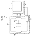
- FIG. 13 is a block diagram schematically illustrating a display control system of an electronic apparatus according to a third embodiment of the invention.
- an active-matrix-type transflective liquid crystal display device which is an example of an electro-optical device, using TFDs (thin film diodes) as two-terminal switching elements and an electronic apparatus using the liquid crystal display device, but the invention is not limited thereto.
- TFDs thin film diodes
- the number and scale of components or members differ from the actual number and scale thereof in order for them to have recognizable sizes.
- a liquid crystal display device 1 includes a liquid crystal panel 2 and a circuit board 3 connected to the liquid crystal panel 2 .
- the liquid crystal display device 1 may be provided with additional units including an illuminating device (not shown), such as a backlight, if necessary.
- the liquid crystal panel 2 includes a pair of substrates 5 and 6 which are bonded to each other with a sealing member 4 interposed therebetween and an electro-optical material injected in a space between the substrates 5 and 6 , for example, TN (twisted nematic) liquid crystal 7 .
- TN twisted nematic
- each pixel 8 has rectangular sub-pixels 9 R, 9 G, and 9 B for respectively displaying red, green, and blue, and the sub-pixels 9 R, 9 G, and 9 B are formed in a row along the X direction, with first light shielding layers 14 a interposed among the sub-pixels.
- the sub-pixel 9 R includes a transmissive display region 10 R transmitting light emitted from a backlight (not shown) which is provided on a surface of the substrate 5 opposite to the liquid crystal 7 to perform color display and a reflective display region 11 R having a reflective film, which will be described later, provided therein.
- the reflective display region 11 R has an effective reflective display region 13 R which reflects light incident on the substrate 5 from the substrate 6 to perform monochromatic display and a flat region 14 R, which will be described later, other than the effective reflective display region 13 R.
- reflective display is performed by the effective reflective display region 13 R and the flat region 14 R.
- a transmissive display region 10 R is provided in a portion (a lower side of FIG. 2 and a right side of FIG. 3 ) of the sub-pixel 9 R in the Y direction of FIG. 2 or 3
- the effective reflective display region 13 R is provided in another portion (an upper side of FIG. 2 and a left side of FIG. 3 ) of the sub-pixel 9 R in the Y direction of FIG. 2 or 3 .
- the sub-pixel 9 R includes an underlayer 15 R provided in the effective reflective display region 13 R, a reflective film 16 R which is provided in the reflective display region 11 R and has a flat portion 17 R provided in the flat region 14 R adjacent to the transmissive display region 10 R, a colored layer 18 R provided at least in the transmissive display region 10 R, a planarizing layer 19 for planarizing a surface of the reflective film 16 R facing the liquid crystal 7 , a cell thickness adjusting layer 20 for adjusting the thickness of the liquid crystal 7 in the Z direction, and a scanning electrode 21 .
- the underlayer 15 R is provided on a surface of the substrate 5 facing the liquid crystal 7 in the effective reflective display region 13 R.
- the underlayer 15 R is formed of, for example, resin. A plurality of uneven portions is provided in the underlayer 15 R.
- the reflective film 16 R is provided in the reflective display region 11 R.
- the reflective film 16 R is formed of, for example, aluminum or an aluminum alloy.
- the reflective film 16 R provided in the effective reflective display region 13 R has an uneven shape corresponding to the uneven shape of the underlayer 15 R. In this way, light incident from the substrate 6 can be scattered by the reflective film 16 R to be reflected therefrom.
- the flat portion 17 R of the reflective film 16 R extends from the reflective film 16 R provided in the effective reflective display region 13 R to the flat region 14 R so as to be provided on the surface of the substrate 5 facing the liquid crystal 7 without the underlayer interposed therebetween in the flat region 14 R.
- the reflective film 16 R and the flat portion 17 R are integrally formed of, for example, aluminum.
- the flat portion 17 R has a surface substantially parallel to the surface of the substrate 5 facing the liquid crystal 7 .
- a width a of the flat portion 17 R in the Y direction is within a range of 1 to 10 ⁇ m, preferably, a range of 2 to 6 ⁇ m, and more preferably, 4 ⁇ m. That is, a gap between the transmissive display region 10 R and the effective reflective display region 13 R is within a range of 1 to 10 ⁇ m.
- a flat portion 27 B extending from a reflective film 26 B provided in an effective reflective display region 13 B is provided on the surface of the substrate 5 facing the liquid crystal 7 in the vicinity of a boundary between the transmissive display region 10 R of the sub-pixel 9 R and the effective reflective display region 13 B of a sub-pixel 9 B adjacent to the transmissive display region 10 R.
- the flat portions 17 R and 27 B are provided on the substrate 5 .
- an underlayer may be formed on the substrate 5 and the flat portions 17 R and 27 B may be formed on the underlayer.
- a red colored layer 18 R is provided on the surface of the substrate 5 facing the liquid crystal 7 in the transmissive display region 10 R.
- an end of the colored layer 18 R adjacent to the flat region 14 R is laminated on the flat portion 17 R.
- the colored layer 18 R may not be formed on the flat portion 17 R.
- a portion of the colored layer 18 R is formed on the flat portion 17 R, considering the error in manufacture.
- the planarizing layer 19 is provided on surfaces of the reflective film 16 R, the flat portion 17 R, and the colored layer 18 R facing the liquid crystal 7 .
- the planarizing layer 19 is formed of, for example, acrylic resin.
- the planarizing layer 19 has a flat surface facing the liquid crystal 7 .
- the cell thickness adjusting layer 20 is provided on a surface of the planarizing layer 19 facing the liquid crystal 7 in the effective reflective display region 13 R and the flat region 14 R.
- the cell thickness adjusting layer 20 is formed of, for example, acrylic resin.
- the cell thickness adjusting layer 20 causes the thickness of the liquid crystal 7 in the Z direction in the effective reflective display region 13 R to be smaller than the thickness of the liquid crystal 7 in the Z direction in the transmissive display region 10 R.
- the scanning electrode 21 is provided on surfaces of the cell thickness adjusting layer 20 and the planarizing layer 19 facing the liquid crystal 7 in the X direction of FIG. 3 in the transmissive display region 10 R, the effective reflective display region 13 R, and the flat region 14 R.
- the scanning electrode 21 is formed of, for example, ITO (indium tin oxide).
- an alignment film (not shown) formed of, for example, polyimide resin is formed on the scanning electrode 21 , and a polarizing plate (not shown) is provided on a surface of the substrate 5 opposite to the liquid crystal 7 .
- the first light shielding layer 14 a is formed between, for example, adjacent sub-pixels 9 R and 9 G by laminating colored layers.
- a second light shielding layer 14 b is provided on a surface of the flat portion 27 B facing the liquid crystal 7 between the transmissive display region 10 R and the effective reflective display region 13 B of the sub-pixel 9 B adjacent to the transmissive display region 10 R.
- the second light shielding layer 14 b is formed by laminating an end portion of the colored layer 18 R provided in the transmissive display region 10 R, facing the effective reflective display region 13 B, on another colored layer.
- the sub-pixels 9 G and 9 B have the same structure as the sub-pixel 9 R except that green and blue colored materials are used to perform green and blue display, and thus a description thereof will be omitted.
- the substrate 6 has a plurality of pixel electrodes 22 arranged in a matrix, a plurality of signal electrodes 23 (which is shown in FIG. 1 , but is not shown in FIG. 3 ) which extend in strip shapes so as to intersect the scanning electrodes 21 at boundary regions between the pixel electrodes 22 , and TFDs 24 connected to the pixel electrodes 22 and the signal electrodes 23 on a surface thereof facing the liquid crystal 7 .
- an alignment film (not shown) is formed on surfaces of the pixel electrodes 22 facing the liquid crystal 7 .
- the pixel electrodes 22 are formed of a transparent conductive material, such as ITO. Similar to the substrate 5 , for example, a polarizing plate (not shown) is provided on a surface of the substrate 6 opposite to the liquid crystal.
- the substrates 5 and 6 are plate members formed of a transmissive material, such as glass or synthetic resin.
- the substrate 5 has a protruding portion 26 extending from the edge of the substrate 6 (hereinafter, referred to as a ‘protruding portion’).
- the protruding portion 26 is provided with scanning electrode wiring lines 27 and signal electrode wiring lines 28 composed of the scanning electrodes 21 and the scanning electrodes 23 extending from a region surrounded the sealing member 4 and a liquid crystal driving IC 29 for supplying, for example, a liquid crystal driving current to the scanning and signal electrode wiring lines 27 and 28 .
- the protruding portion 26 is provided with a plurality of electrode terminals (not shown) provided in a mounting region of the substrate 5 corresponding to a mounting surface of the liquid crystal driving IC 29 and a plurality of input terminals (not shown) for inputting a current from the circuit board 3 to the liquid crystal driving IC 29 .
- the electrode terminals are connected to the scanning electrode wiring lines 27 and the signal electrode wiring lines 28 .
- the protruding portion 26 includes external connection terminals (not shown) for receiving a current from the circuit board 3 and input wiring lines 30 for supplying the current from the outside to the input terminals.
- the signal electrodes 23 are formed of a metallic material, such as Ta, Cr, or TaW.
- the circuit board 3 is constituted by forming, for example, a wiring pattern 32 on a base substrate 31 .
- the base substrate 31 is a film member having flexibility, and the wiring pattern 32 is formed of, for example, copper.
- terminals are formed on a side of the base substrate 31 facing the protruding portion 26 so as to be connected to the external connection terminals through, for example, ACF.
- FIG. 4 is a flow chart illustrating a process of manufacturing the liquid crystal display device 1 according to the first embodiment.
- the substrate 5 is cleaned and dried, and, for example, a positive photosensitive resin is applied onto the substrate 5 to form the underlayer 15 R having an uneven pattern thereon in the effective reflective display region 13 R (S 1 ).
- an aluminum film is formed with a predetermined thickness so as to cover the substrate 5 and underlayers 15 R and 15 B by using, for example, a sputtering method. Portions of the reflective film is removed by, for example, etching to form a plurality of apertures through which light passes, thereby forming the reflective films 16 R and 26 B having the flat portions 17 R and 27 B, respectively (S 2 ).
- the flat portion 17 R is integrally formed with the reflective film 16 R in the flat region 14 R so as to have a width a of 1 to 10 ⁇ m in the Y direction.
- the flat portion 27 B is integrally formed with the reflective film 26 B in the flat region 24 R so as to have a width a of 1 to 10 ⁇ m in the Y direction.
- a material forming a colored layer 14 c is applied in the vicinity of the boundary between the transmissive display region 10 R of the sub-pixel 9 R and the effective reflective display region 13 B of the sub-pixel 9 B adjacent to the transmissive display region 10 R in the Y direction to form the second light shielding layer 14 b therein, and a material forming the colored layer 18 R is applied so as to overlap the colored layer 14 c and the surface of the substrate 5 facing the liquid crystal 7 in the transmissive display region 10 R (S 3 ).
- the material forming the colored layer 18 R flows on the flat portion 17 R to protrude from the flat region 14 R, there is no fear that the colored layer 18 R will be provided in the effective reflective display region 13 R.
- a gap (the width a of the flat portion 17 R in the Y direction) between the transmissive display region 10 R and the effective reflective display region 13 R is set such that the colored layer 18 R is not provided in the effective reflective display region 13 R.
- the green colored layer 18 G and the blue colored layer 18 B are formed, and the first and second light shielding layers 14 a and 14 b are formed in the same manner as described above.
- the second light shielding layer 14 b may not be provided.
- the planarizing layer 19 is formed in the transmissive display region 10 R, the effective reflective display region 13 R, and the flat region 14 R, and a transparent photosensitive resin is applied on a surface of the planarizing layer 19 facing the liquid crystal 7 in the effective reflective display region 13 R and the flat region 14 R to form the cell thickness adjusting layer 20 .
- the thickness of the liquid crystal 7 in the Z direction in the effective reflective display region 13 R is smaller than the thickness of the liquid crystal 7 in the Z direction in the transmissive display region 10 R.
- a thin film made of, for example, ITO is formed on the colored layer 18 R and the cell thickness adjusting layer 20 and is then patterned, thereby forming the scanning electrode 21 (S 5 ).
- an alignment film (not shown) is formed so as to cover the scanning electrodes 21 , and a rubbing process is performed thereon.
- the pixel electrodes 22 , the signal electrodes 23 , and the TFDs 24 are formed on the substrate 6 opposite to the substrate 5 . Then, an alignment film (not shown) is formed so as to cover the pixel electrodes 22 , and a rubbing process is performed thereon (S 6 ).
- the sealing member 4 is provided on the substrate 5 , and the substrates 5 and 6 are bonded to each other such that the first and second light shielding layers 14 a and 14 b are opposite to the boundary regions between the pixel electrodes 22 formed on the substrate 6 (S 7 ).
- the liquid crystal 7 is injected through an injection hole formed in the sealing member 4 , and the injection hole is sealed.
- polarizing plates are formed on outer surfaces of the substrates 5 and 6 , and the circuit board 3 is connected to the liquid crystal panel 2 , thereby manufacturing the liquid crystal display device 1 (S 8 ).
- the reflective film 16 R is provided in the reflective display region 11 R and has the flat portion 17 R formed in the flat region 14 R of the reflective display region 11 R adjacent to the transmissive display region, and the colored layer 18 R is formed only between the flat region 14 R and the transmissive display region 10 R. Therefore, even when the colored layer 18 R to be provided in only the transmissive display region 10 R protrudes to the flat region 14 R of the reflective display region 11 R due to a manufacturing error, the colored layer 18 R can be provided to protrude to only the flat region 14 R, but not to protrude to the uneven effective reflective display region 13 R.
- This structure makes it possible to ensure the quality of color display by the colored layer 18 R provided in the transmissive display region 10 R and to prevent poor monochromatic reflective display, resulting in an improvement in the quality of monochromatic display in the reflective display region 11 R.
- the light When light is incident on the flat region 14 R, the light can be mirror-reflected therefrom without dispersion, which makes it possible to prevent the colored layer 18 R protruding to the flat region 14 R from contributing to display.
- the flat portion 17 R can be formed of the same material as that of the reflective film 16 R in the flat region 14 R at the same time when the reflective film 16 R is provided in the effective reflective display region 13 R. Thus, it is possible to reduce the number of manufacturing processes and manufacturing costs.
- the reflective film 16 R provided in the effective reflective display region 13 R other than the flat region 14 R in the reflective display region 11 R has an uneven surface, the reflective film 16 R can contribute to reflective display by distributed light.
- the sub-pixel 9 B is provided adjacent to the sub-pixel 9 R, and the reflective film 26 B has the flat portion 27 B provided in the flat region 24 R between the transmissive display region 10 R of the sub-pixel 9 R and the reflective display region 11 B of the sub-pixel 9 B.
- This structure makes it possible to prevent the colored layer 18 R for performing color display from protruding to the effective reflective display region 13 B through the flat region 24 R and thus to improve the quality of reflective display.
- the flat portion 17 R of the reflective film 16 R can be simultaneously formed with the flat portion 27 B of the reflective film 26 B, which results in a reduction in the number of manufacturing processes.
- the second light shielding layer 14 b formed by laminating the colored layer 18 R on a colored layer having a different color from that of the colored layer 18 R is provided between the transmissive display region 10 R of the sub-pixel 9 R and the effective reflective display region 13 B of the sub-pixel 9 B adjacent to the sub-pixel 9 R. Therefore, the colored layer 18 R for performing color display can be used for forming the second light shielding layer 14 b , which makes it possible to further reduce manufacturing costs as compared with the case in which the second light shielding layer 14 b is formed of a member different from the colored layer 14 b.
- the transmissive display region 10 R is provided in a portion (a lower side of FIG. 2 and a right side of FIG. 3 ) of the sub-pixel 9 R in the Y direction of FIG. 2
- the effective reflective display region 13 R is provided in the other portion (an upper side of FIG. 2 and a left side of FIG. 3 ) of the sub-pixel 9 R in the Y direction of FIG. 2
- the side of the flat region 14 R facing the transmissive display region 10 R has a linear shape. Therefore, it is possible to decrease the length of the side of the flat region 14 R facing the transmissive display region 10 R as compared with the case in which the flat region is provided in a curved line and thus to reduce the area of the flat region 14 R. As a result, it is possible to prevent a reduction in the brightness of reflective display and to improve the quality of monochromatic display in the effective reflective display region 13 R.
- the width a (the width a of the flat portion 17 R in the Y direction) of the flat region 14 R is within a range of 1 to 10 ⁇ m, which makes it possible to reliably prevent the colored layer from protruding to the effective reflective display region 13 R through the flat region 14 R and thus to prevent reflective display from being excessively dark by the flat region 14 R.
- the uneven underlayer 15 R is provided in the reflective display region 11 R except the flat region 14 R to give a scattering function to the reflective film 16 R.
- This structure makes it possible to allow scattered light to contribute to reflective display and to form the flat portion 17 R not contributing to reflective display in the flat region 14 R, corresponding to a region where the underlayer 15 R is not formed.
- the flat region 14 R is a mirror-reflective region, poor reflective color display does not occur therein even when the colored layer 18 R protrudes toward the flat region 14 R.
- the underlayer 15 R is provided between the substrate 5 and the reflective film 16 R in the effective reflective display region 13 R, but is not provided in the flat region 14 R, and the flat portion 17 R is provided on the substrate 5 without the underlayer 15 R interposed therebetween. Therefore, the flat portion 17 R can be formed in the region where the underlayer 15 R is not formed. In addition, since the flat surface of the substrate 5 is used to provide the flat portion 17 R, the flat portion 17 R can be more reliably provided.
- the reflective film 16 R and the colored layer 18 R may be provided on different substrates.
- the reflective film 16 R provided in the effective reflective display region 13 R and the flat region 14 R partially overlaps the colored layer 18 R provided in a portion of the flat region 14 R and the transmissive display region 10 R in the flat region 14 R.
- liquid crystal display device according to a second embodiment of the invention will be described.
- a description will be made of an active-matrix-type transflective liquid crystal display device using TFTs (thin film transistors) as three-terminal switching elements.
- TFTs thin film transistors
- the same components as those in the second embodiment have the same reference numerals, and a description thereof will be omitted. Therefore, a description will be made centered on different components.
- FIG. 5 is a plan view schematically illustrating pixels of a liquid crystal panel of the liquid crystal display device according to the second embodiment.
- FIG. 6 is a cross-sectional view of a pixel of the liquid crystal panel, taken along the line VI-VI of FIG. 5 .
- the reflective film 16 R provided in the reflective display region 11 R has the flat portion 17 R in the flat region 14 R, and is provided on the surface of the substrate 5 facing the liquid crystal 7 .
- a reflective film 49 R which will be described later, is provided on a surface of the substrate 5 facing the liquid crystal 7
- a light shielding portion 50 R is provided on a surface of the substrate 6 facing the liquid crystal 7 , corresponding to a flat portion 37 R of the reflective film 49 R.
- a plurality of pixels 35 which are units for displaying, for example, characters, are provided on the substrate 5 in the X and Y directions. As shown in FIG. 5 , each pixel 35 has three rectangular sub-pixels 40 R, 40 G, and 40 B for respectively displaying red, green, and blue, and the sub-pixels 40 R, 40 G, and 40 B are formed in a row along the X direction, with first light shielding layers 14 a interposed among the sub-pixels.
- a transmissive display region 41 R is provided in a portion (a lower side of FIG. 5 and a right side of FIG. 6 ) of the sub-pixel 40 R in the Y direction of FIG. 5 , and a reflective display region 42 R having a reflective film, which will be described later, formed therein is provided in another portion (an upper side of FIG. 5 and a left side of FIG. 6 ) of the sub-pixel 40 R in the Y direction of FIG. 5 .
- the reflective display region 42 R includes an effective reflective display region 43 R for reflecting light incident on the substrate 5 from the substrate 6 to perform monochromatic display and a light shielding region 44 R (which will be described later), which is a portion of the reflective display region 42 R other than the effective reflective display region 43 R.
- the substrate 5 has contact electrodes 45 R each provided in the effective reflective display region 43 R and a portion of the light shielding region 44 R to electrically connect the reflective film 49 R, a transparent electrode 46 R, and a TFT 47 , the transparent electrodes 46 R each provided in the transmissive display region 41 R and a portion of the light shielding region 44 R, TFTs 47 each electrically connected to the contact electrode 45 R, an underlayer 48 R provided on a surface of the substrate 5 facing the liquid crystal 7 in the effective reflective display region 43 R, and the reflective film 49 R which is formed on the underlayer 48 R and has the flat portion 37 R provided in the light shielding region 44 R provided thereon.
- the substrate 6 has the light shielding portions 50 R provided on a surface thereof facing the liquid crystal 7 in the light shielding region 44 R, light shielding portions 51 R, which will be described later, colored layers 52 R provided on the surface thereof facing the liquid crystal 7 in at least the transmissive display region 41 R, a planarizing layer 53 , and a common electrode 54 provided thereon, which will be described later.
- the contact electrode 45 R is provided on the surface of the substrate 5 facing the liquid crystal 7 in the effective reflective display region 43 R and a portion of the light shielding region 44 R. An end portion of the contact electrode 45 R is provided in the light shielding region 44 R.
- the contact electrode 45 R is formed of a metallic material, such as chrome.
- the transparent electrode 46 R is provided on the surface of the substrate 5 facing the liquid crystal 7 in the effective reflective display region 41 R and a portion of the light shielding region 44 R. As shown in FIG. 6 , an end portion of the transparent electrode 46 R is laminated on the end portion of the contact electrode 45 R in the light shielding region 44 R.
- the transparent electrode 46 R is formed of, for example, ITO.
- Each TFT 47 includes gate and source electrodes (not shown) and is electrically connected to the contact electrode 45 R.
- the underlayer 48 R is provided on the surface of the substrate 5 facing the liquid crystal 7 so as to be laid across the effective reflective display region 43 R and a portion of the light shielding region 44 R. A plurality of uneven portions is provided in the underlayer 48 R.
- the reflective film 49 R is formed on a surface of the underlayer 48 R facing the liquid crystal 7 .
- the reflective film 49 R is formed of, for example, aluminum or an aluminum alloy.
- the reflective film 49 R has an uneven shape corresponding to the uneven shape of the underlayer 48 R.
- An end portion of the reflective film 49 R in the light shielding region 44 R is electrically connected to a connecting portion between the contact electrode 45 R and the transparent electrode 46 R and constitutes the flat portion 37 R serving as a reflective electrode.
- the light shielding portion 50 R is provided on the surface of the substrate 6 facing the liquid crystal 7 in the light shielding region 44 R without the underlayer interposed therebetween.
- the light shielding portion 50 R has a surface substantially parallel to the surface of the substrate 6 facing the liquid crystal 7 .
- a width a of the light shielding portion 50 R in the Y direction is within a range of 1 to 10 ⁇ m.
- the light shielding portion 50 R is formed of a metallic material, such as aluminum.
- the light shielding portion 51 R is provided on the surface of the substrate 6 facing the liquid crystal 7 in the vicinity of a boundary between the transmissive display region 41 R of the sub-pixel 40 R and the effective reflective display region 43 B of the sub-pixel 40 B adjacent to the transmissive display region 41 R in the Y direction.
- the width a of the light shielding portion 51 R in the Y direction is within a range of 1 to 10 ⁇ m.
- the light shielding portion 51 R is formed of a metallic material, such as aluminum.
- the width of the transmissive display region 41 R is determined by the light shielding portions 50 R and 51 R.
- the red colored layer 52 R is provided in at least the transmissive display region 41 R on the surface of the substrate 6 facing the liquid crystal 7 . Both ends of the colored layer 52 R in the Y direction are laminated on portions of the light shielding portions 50 R and 51 R. Alternatively, the colored layer 52 R may be formed so as not to be laminated on the light shielding portions 50 R and 51 R. However, in order to prevent a region not having the colored layer 52 R therein from being formed in the transmissive display region 41 R due to an error in manufacture, a portion of the colored layer 52 R is formed on the light shielding portion 50 R, considering the error in manufacture.
- the planarizing layer 53 is provided on surfaces of the substrate 6 , the light shielding portion 50 R, and the colored layer 52 R facing the liquid crystal 7 .
- the planarizing layer 53 has a flat surface facing the liquid crystal 7 .
- the planarizing layer 53 is formed of, for example, acrylic resin.
- the common electrode 54 is provided on a surface of the planarizing layer 53 facing the liquid crystal 7 .
- the common electrode 54 is formed of a transparent conductive material, such as ITO.
- an alignment film (not shown) is provided on a surface of the common electrode 54 facing the liquid crystal 7 .
- a polarizing plate (not shown) is provided on the surface of the substrate 6 opposite to the liquid crystal 7 .
- the reflective film 49 R and the flat portion 37 R are provided on the surface of the substrate 5 facing the liquid crystal 7
- the light shielding portion 50 R is provided on the surface of the substrate 6 facing the liquid crystal 7 so as to correspond to the flat portion 37 R. Therefore, even when the colored layer 52 R to be provided in the transmissive display region 41 R protrudes toward the light shielding region 44 R due to a manufacturing error, the colored layer 52 R does not protrude to the effective reflective display region 43 R, and is hidden by the light shielding portion 50 R, as viewed from the light transmission side, which makes it possible to improve the quality of monochromatic display in the reflective display region 43 R.
- a light shielding portion 51 R capable of shielding light is provided in the vicinity of a boundary between the transmissive display region 41 R of the sub-pixel 40 R and the effective reflective display region 43 B of the sub-pixel 40 B adjacent to the transmissive display region 41 R.
- the light shielding portions 50 R and 51 R can be formed at the same time between the transmissive display region 41 R and the effective reflective display region 43 R and in the vicinity of the boundary between the transmissive display region 41 R of the sub-pixel 40 R and the effective reflective display region 43 B of the sub-pixel 40 B, respectively.
- FIG. 7 is a cross-sectional view of a pixel of a liquid crystal panel of a liquid crystal display device according to a first modification.
- the flat portion 17 R is provided on the surface of the substrate 5 facing the liquid crystal 7 so as to extend from the reflective film 16 R provided in the effective reflective display region 13 R to the flat region 14 R.
- a flat portion 67 R which will be described later, is formed of a different material from a reflective film 66 R provided in an effective reflective display region 63 R on a surface of the substrate 5 facing the liquid crystal 7 .
- the sub-pixel 60 R has a rectangular transmissive display region 61 R transmitting light emitted from a backlight (not shown) which is provided on a surface of the substrate 5 opposite to the liquid crystal 7 to perform color display and a reflective display region 62 R, which will be described later, provided therein.
- the reflective display region 62 R has an effective reflective display region 63 R which reflects light incident on the substrate 5 from the substrate 6 to perform monochromatic display and a flat region 64 R other than the effective reflective display region 63 R.
- the sub-pixel 60 R includes an underlayer 65 R provided in the effective reflective display region 63 R, a reflective film 66 R formed on the underlayer 65 R, a flat portion 67 R provided in the flat region 64 R, a colored layer 18 R provided in at least the transmissive display region 61 R, a planarizing layer 19 for planarizing a surface of the reflective film 66 R facing the liquid crystal 7 , a cell thickness adjusting layer 20 for adjusting the thickness of the liquid crystal 7 in the Z direction, and a scanning electrode 21 .
- the underlayer 65 R is provided on a surface of the substrate 5 facing the liquid crystal 7 in the effective reflective display region 63 R, but is not provided in the flat region 64 R.
- the underlayer 65 R is formed of, for example, resin. A plurality of uneven portions is provided in the underlayer 65 R.
- the reflective film 66 R is formed on a surface of the underlayer 65 R facing the liquid crystal 7 , but is not provided in the flat region 64 R.
- the reflective film 66 R is formed of, for example, aluminum or an aluminum alloy.
- the reflective film 66 R has an uneven shape corresponding to the uneven shape of the underlayer 65 R. In this way, light incident from the substrate 6 can be scattered by the reflective film 66 R to be reflected therefrom.
- the flat portion 67 R is formed of, for example, a metallic material different from that forming the reflective film 66 R provided in the effective reflective display region 63 R on the surface of the substrate 5 facing the liquid crystal 7 .
- the flat portion 67 R is provided on the surface of the substrate 5 facing the liquid crystal 7 without the underlayer 65 R interposed therebetween in the flat region 64 R.
- the flat portion 67 R is formed of, for example, aluminum.
- the flat portion 67 R has a surface substantially parallel to the surface of the substrate 5 facing the liquid crystal 7 .
- a width a of the flat portion 67 R in the Y direction is within a range of 1 to 10 ⁇ m.
- a red colored layer 18 R is provided in at least the transmissive display region 61 R on the surface of the substrate 5 facing the liquid crystal 7 .
- an end of the colored layer 18 R adjacent to the flat region 64 R is laminated on the flat portion 67 R.
- the end of the colored layer 18 R is formed on the flat portion 67 R, but the colored layer 18 R may not be formed on the flat portion 67 R.
- a portion of the colored layer 18 R is formed on the flat portion 67 R, considering the error in manufacture.
- the planarizing layer 19 is provided on surfaces of the reflective film 66 R, the flat portion 67 R, and the colored layer 18 R facing the liquid crystal 7 .
- the planarizing layer 19 is formed of, for example, acrylic resin.
- the planarizing layer 19 has a flat surface facing the liquid crystal 7 .
- the cell thickness adjusting layer 20 and the scanning electrode 21 have the same structure as those in the first embodiment, and thus a description thereof will be omitted.
- the sub-pixels 60 G and 60 B have the same structure as that of the sub-pixel 60 R except that green and blue colored materials are used to perform green and blue display, and thus a description thereof will be omitted.
- the substrate 6 has the same structure as that in the first embodiment, and a description thereof will be omitted.
- the flat portion 67 R is formed of a metallic material different from that forming the reflective film 66 R provided on the surface of the substrate 5 in the effective reflective display region 63 R. Therefore, the flat portion 67 R can be simultaneously formed with metal wiring lines, and thus a liquid crystal display device can be manufactured without an increase in manufacturing costs.
- the reflective film 66 R of the effective reflective display region 63 R can be formed of, for example, a metallic material, and the flat portion 67 R can be formed of a material (for example, white pigment) other than the metallic material.
- the flat portion 17 R is provided on the surface of the substrate 5 facing the liquid crystal 7 so as to extend from the reflective film 16 R provided in the effective reflective display region 13 R to the flat region 14 R.
- the underlayer 15 R having unevenness on a surface thereof is formed in the effective reflective display region 13 R and flat region 14 R on the surface of the substrate 5 facing the liquid crystal 7 , and a planarizing film 15 h made of the same resin material as that forming the underlayer 15 R is formed on the uneven underlayer 15 R in the flat region 14 R to planarize the uneven surface, so that a flat surface 14 h is formed in the flat region 14 R by the planarizing film 15 h made of resin, as shown in FIG. 9 .
- the side of the flat region 14 R adjacent to the transmissive display region 10 R has a linear shape, but the forming positions of the transmissive display region and the flat region in a sub-pixel are not limited thereto.
- the transmissive display region may be formed in an island shape in the reflective display region, and the flat region may be provided between the reflective display region and the transmissive display region.
- the reflective display region may be formed in an island shape in the transmissive display region, and the flat region may be provided between the reflective display region and the transmissive display region. In these cases, it is possible to prevent the deterioration of display quality depending on the deviation of the forming positions of the transmissive display region and the reflective display region.
- the following structures can be considered: a structure in which a reflective film is provided in an island shape in a sub-pixel, regions where the reflective film is provided are used as an effective reflective display region and a flat region, and a transmissive display region is provided so as to surround the island-shaped reflective film; and a structure in which apertures are formed in a reflective film, the apertures are used as transmissive display regions, and effective reflective display regions and flat regions are provided so as to surround the apertures.
- FIG. 13 is a block diagram schematically illustrating the overall structure of a display control system of the electronic apparatus according to the third embodiment of the invention.
- an electronic apparatus 300 includes, as a display control system, the liquid crystal panel 2 and a display control unit 390 .
- the display control unit 390 includes a display information output source 391 , a display information processing circuit 392 , a power supply circuit 393 , and a timing generator 394 .
- the liquid crystal panel 2 has a driving circuit 361 including the liquid crystal driving IC 29 for driving a display region I.
- the display information output source 391 has a memory composed of a ROM (read only memory) or a RAM (random access memory), a storage unit composed of, for example, a magnetic recording disk or an optical recording disk, and a tuning circuit for tuning and outputting digital image signals.
- the display information output source 391 supplies display information to the display information processing circuit 392 in the form of image signals having a predetermined format, on the basis of various clock signals generated by the timing generator 394 .
- the display information processing circuit 392 includes various well-known circuits, such as a serial-parallel conversion circuit, an amplification/inversion circuit, a rotation circuit, a gamma correction circuit, and a clamp circuit.
- the display information processing circuit 392 processes input display information to supply the processed image information to the driving circuit 361 together with a clock signal CLK.
- the power supply circuit 393 supplies a predetermined voltage to the above-mentioned components.
- the electronic apparatus since the electronic apparatus has the liquid crystal display device 1 capable of improving the quality of monochromatic display in the effective reflective display region 13 R while ensuring the quality of monochromatic display in the transmissive display region 10 R, it can have good display characteristic.
- the invention can be applied to various electronic apparatuses, such as a cellular phone, a personal computer, a digital still camera, a touch panel, a projector, a liquid crystal television, a view-finder-type/monitor-direct-view-type videotape recorder, a car navigation apparatus, a pager, an electronic organizer, an electronic calculator, a word processor, a workstation, a television phone, and a POS terminal which are equipped with the liquid crystal display devices.
- a cellular phone such as a personal computer, a digital still camera, a touch panel, a projector, a liquid crystal television, a view-finder-type/monitor-direct-view-type videotape recorder, a car navigation apparatus, a pager, an electronic organizer, an electronic calculator, a word processor, a workstation, a television phone, and a POS terminal which are equipped with the liquid crystal display devices.
- a cellular phone such as a cellular phone, a personal computer, a digital still camera
- the liquid crystal display device 1 using TFDs and the liquid crystal display device using TFTs are used, but the invention is not limited thereto.
- the invention may be applied to a passive matrix liquid crystal display device.
- the invention may be applied to various electro-optical devices, such as an electrophoresis display device, and electronic apparatuses including touch panels.
Landscapes
- Physics & Mathematics (AREA)
- Nonlinear Science (AREA)
- Mathematical Physics (AREA)
- Chemical & Material Sciences (AREA)
- Crystallography & Structural Chemistry (AREA)
- General Physics & Mathematics (AREA)
- Optics & Photonics (AREA)
- Liquid Crystal (AREA)
Abstract
Description
Claims (12)
Applications Claiming Priority (2)
| Application Number | Priority Date | Filing Date | Title |
|---|---|---|---|
| JP2005-057116 | 2005-03-02 | ||
| JP2005057116A JP4127272B2 (en) | 2005-03-02 | 2005-03-02 | Electro-optical device substrate, electro-optical device, and electronic apparatus |
Publications (2)
| Publication Number | Publication Date |
|---|---|
| US20060197895A1 US20060197895A1 (en) | 2006-09-07 |
| US7889294B2 true US7889294B2 (en) | 2011-02-15 |
Family
ID=36943773
Family Applications (1)
| Application Number | Title | Priority Date | Filing Date |
|---|---|---|---|
| US11/351,180 Active 2027-04-25 US7889294B2 (en) | 2005-03-02 | 2006-02-09 | Electro-optical device with transmissive and reflection display regions where the reflection display region has a scatter-reflection and mirror-reflection region |
Country Status (4)
| Country | Link |
|---|---|
| US (1) | US7889294B2 (en) |
| JP (1) | JP4127272B2 (en) |
| KR (1) | KR100756100B1 (en) |
| CN (1) | CN100432767C (en) |
Families Citing this family (3)
| Publication number | Priority date | Publication date | Assignee | Title |
|---|---|---|---|---|
| JP4670102B2 (en) * | 2006-11-21 | 2011-04-13 | ワン ラップトップ パー チャイルド アソシエイション インク. | Dual mode display |
| US8194211B2 (en) * | 2008-03-18 | 2012-06-05 | Nlt Technologies, Ltd. | Transflective liquid crystal display unit |
| KR20130114996A (en) * | 2012-04-10 | 2013-10-21 | 삼성디스플레이 주식회사 | Display apparatus and fabricating method thereof |
Citations (24)
| Publication number | Priority date | Publication date | Assignee | Title |
|---|---|---|---|---|
| US6008871A (en) * | 1997-01-20 | 1999-12-28 | Seiko Epson Corporation | Transflective liquid crystal display device having a reflective polarizer |
| JP2000111902A (en) | 1998-01-26 | 2000-04-21 | Sharp Corp | Liquid crystal display |
| US6081354A (en) * | 1998-05-15 | 2000-06-27 | E. I. Du Pont De Nemours And Company | Holographic reflector for liquid crystal display |
| US6195140B1 (en) * | 1997-07-28 | 2001-02-27 | Sharp Kabushiki Kaisha | Liquid crystal display in which at least one pixel includes both a transmissive region and a reflective region |
| US6215538B1 (en) | 1998-01-26 | 2001-04-10 | Sharp Kabushiki Kaisha | Liquid crystal display including both color filter and non-color filter regions for increasing brightness |
| JP2002055333A (en) | 2000-08-11 | 2002-02-20 | Seiko Epson Corp | Liquid crystal device substrate, method of manufacturing the same, liquid crystal device and electronic equipment |
| US20030016459A1 (en) * | 2001-07-13 | 2003-01-23 | Keiji Takizawa | Color filter substrate and electro-optical device, manufacturing method for color filter substrate and manufacturing method for electro-optical device, and electronic equipment |
| US20030025977A1 (en) * | 2001-07-27 | 2003-02-06 | Keiji Takizawa | Electro-optical device, color filter substrate and electronic apparatus |
| US20030133059A1 (en) | 2002-01-15 | 2003-07-17 | Chi Mei Optoelectronics Corp. | Liquid crystal display device |
| US6624860B1 (en) | 1998-01-26 | 2003-09-23 | Sharp Kabushiki Kaisha | Color filter layer providing transmitted light with improved brightness and display device using same |
| CN1447155A (en) | 2002-03-26 | 2003-10-08 | 精工爱普生株式会社 | LCD device and electronic equipment |
| JP2003344847A (en) | 2002-05-30 | 2003-12-03 | Optrex Corp | Transflective liquid crystal display panel |
| JP2004037494A (en) | 2002-06-28 | 2004-02-05 | Seiko Epson Corp | Electro-optical device substrate, electro-optical device substrate manufacturing method, electro-optical device, and electronic apparatus |
| JP2004054129A (en) | 2002-07-23 | 2004-02-19 | Seiko Epson Corp | Liquid crystal display and electronic equipment |
| JP2004077544A (en) | 2002-08-09 | 2004-03-11 | Seiko Epson Corp | Electro-optical devices and electronic equipment |
| JP2004093670A (en) | 2002-08-29 | 2004-03-25 | Casio Comput Co Ltd | Liquid crystal display device |
| JP2004093781A (en) | 2002-08-30 | 2004-03-25 | Seiko Epson Corp | Liquid crystal display |
| JP2004109777A (en) | 2002-09-20 | 2004-04-08 | Seiko Epson Corp | Liquid crystal display device and electronic device |
| US20040252262A1 (en) | 2003-06-10 | 2004-12-16 | Lg. Philips Lcd Co., Ltd. | Transflective liquid crystal display device |
| US20050024559A1 (en) * | 2003-03-13 | 2005-02-03 | Seiko Epson Corporation | Liquid crystal display device and electronic apparatus |
| US20050083453A1 (en) * | 2003-09-10 | 2005-04-21 | Tomoyuki Nakano | Electro-optical device, color filter substrate, method of manufacturing electro-optical device, and electronic apparatus |
| JP2005181604A (en) | 2003-12-18 | 2005-07-07 | Seiko Epson Corp | Color filter substrate, liquid crystal display device and electronic device |
| US7050132B2 (en) * | 1997-12-26 | 2006-05-23 | Sharp Kabushiki Kaisha | Liquid crystal display |
| US7298439B2 (en) * | 2001-09-25 | 2007-11-20 | Seiko Epson Corporation | Transflective liquid crystal device with particular color filter thickness adjusting layer stacking and reflective and electronic apparatus using the same |
Family Cites Families (5)
| Publication number | Priority date | Publication date | Assignee | Title |
|---|---|---|---|---|
| US6407786B1 (en) | 1999-06-09 | 2002-06-18 | Sharp Kabushiki Kaisha | Liquid crystal display device and method for fabricating the same |
| JP2001183649A (en) * | 1999-12-27 | 2001-07-06 | Nec Corp | Reflection type color liquid crystal display device |
| JP3961945B2 (en) * | 2002-12-27 | 2007-08-22 | 株式会社アドバンスト・ディスプレイ | Liquid crystal display |
| JP3918765B2 (en) * | 2003-04-21 | 2007-05-23 | セイコーエプソン株式会社 | Liquid crystal display device and electronic device |
| JP2005173037A (en) | 2003-12-09 | 2005-06-30 | Fujitsu Display Technologies Corp | Liquid crystal display device and manufacturing method thereof |
-
2005
- 2005-03-02 JP JP2005057116A patent/JP4127272B2/en not_active Expired - Lifetime
-
2006
- 2006-02-09 US US11/351,180 patent/US7889294B2/en active Active
- 2006-02-28 KR KR1020060019259A patent/KR100756100B1/en not_active Expired - Lifetime
- 2006-03-02 CN CNB2006100586441A patent/CN100432767C/en not_active Expired - Lifetime
Patent Citations (32)
| Publication number | Priority date | Publication date | Assignee | Title |
|---|---|---|---|---|
| US6008871A (en) * | 1997-01-20 | 1999-12-28 | Seiko Epson Corporation | Transflective liquid crystal display device having a reflective polarizer |
| US6195140B1 (en) * | 1997-07-28 | 2001-02-27 | Sharp Kabushiki Kaisha | Liquid crystal display in which at least one pixel includes both a transmissive region and a reflective region |
| US7050132B2 (en) * | 1997-12-26 | 2006-05-23 | Sharp Kabushiki Kaisha | Liquid crystal display |
| JP2000111902A (en) | 1998-01-26 | 2000-04-21 | Sharp Corp | Liquid crystal display |
| US6215538B1 (en) | 1998-01-26 | 2001-04-10 | Sharp Kabushiki Kaisha | Liquid crystal display including both color filter and non-color filter regions for increasing brightness |
| US6906765B2 (en) | 1998-01-26 | 2005-06-14 | Sharp Kabushiki Kaisha | Color filter layer and display device using the same |
| US7250998B2 (en) | 1998-01-26 | 2007-07-31 | Sharp Kabushiki Kaisha | Color filter layer comprising a transmissive non-color filter region and the transflective display device using the same |
| US6624860B1 (en) | 1998-01-26 | 2003-09-23 | Sharp Kabushiki Kaisha | Color filter layer providing transmitted light with improved brightness and display device using same |
| US20070247570A1 (en) | 1998-01-26 | 2007-10-25 | Sharp Kabushiki Kaisha | Color filter layer and display device using the same |
| US20080002085A1 (en) | 1998-01-26 | 2008-01-03 | Sharp Kabushiki Kaisha | Color filter layer and display device using the same |
| US6081354A (en) * | 1998-05-15 | 2000-06-27 | E. I. Du Pont De Nemours And Company | Holographic reflector for liquid crystal display |
| JP2002055333A (en) | 2000-08-11 | 2002-02-20 | Seiko Epson Corp | Liquid crystal device substrate, method of manufacturing the same, liquid crystal device and electronic equipment |
| US20030016459A1 (en) * | 2001-07-13 | 2003-01-23 | Keiji Takizawa | Color filter substrate and electro-optical device, manufacturing method for color filter substrate and manufacturing method for electro-optical device, and electronic equipment |
| US20030025977A1 (en) * | 2001-07-27 | 2003-02-06 | Keiji Takizawa | Electro-optical device, color filter substrate and electronic apparatus |
| US7298439B2 (en) * | 2001-09-25 | 2007-11-20 | Seiko Epson Corporation | Transflective liquid crystal device with particular color filter thickness adjusting layer stacking and reflective and electronic apparatus using the same |
| US20030133059A1 (en) | 2002-01-15 | 2003-07-17 | Chi Mei Optoelectronics Corp. | Liquid crystal display device |
| CN1447155A (en) | 2002-03-26 | 2003-10-08 | 精工爱普生株式会社 | LCD device and electronic equipment |
| US7119861B2 (en) | 2002-03-26 | 2006-10-10 | Seiko Epson Corporation | Liquid crystal display and electronic apparatus |
| JP2003344847A (en) | 2002-05-30 | 2003-12-03 | Optrex Corp | Transflective liquid crystal display panel |
| JP2004037494A (en) | 2002-06-28 | 2004-02-05 | Seiko Epson Corp | Electro-optical device substrate, electro-optical device substrate manufacturing method, electro-optical device, and electronic apparatus |
| JP2004054129A (en) | 2002-07-23 | 2004-02-19 | Seiko Epson Corp | Liquid crystal display and electronic equipment |
| US20040061817A1 (en) * | 2002-07-23 | 2004-04-01 | Seiko Epson Corporation | Liquid crystal display device and electronic apparatus |
| US7072011B2 (en) | 2002-07-23 | 2006-07-04 | Seiko Epson Corporation | Liquid crystal display device and electronic apparatus |
| JP2004077544A (en) | 2002-08-09 | 2004-03-11 | Seiko Epson Corp | Electro-optical devices and electronic equipment |
| JP2004093670A (en) | 2002-08-29 | 2004-03-25 | Casio Comput Co Ltd | Liquid crystal display device |
| JP2004093781A (en) | 2002-08-30 | 2004-03-25 | Seiko Epson Corp | Liquid crystal display |
| US6757038B2 (en) | 2002-09-20 | 2004-06-29 | Seiko Epson Corporation | Liquid crystal display device and electronic apparatus |
| JP2004109777A (en) | 2002-09-20 | 2004-04-08 | Seiko Epson Corp | Liquid crystal display device and electronic device |
| US20050024559A1 (en) * | 2003-03-13 | 2005-02-03 | Seiko Epson Corporation | Liquid crystal display device and electronic apparatus |
| US20040252262A1 (en) | 2003-06-10 | 2004-12-16 | Lg. Philips Lcd Co., Ltd. | Transflective liquid crystal display device |
| US20050083453A1 (en) * | 2003-09-10 | 2005-04-21 | Tomoyuki Nakano | Electro-optical device, color filter substrate, method of manufacturing electro-optical device, and electronic apparatus |
| JP2005181604A (en) | 2003-12-18 | 2005-07-07 | Seiko Epson Corp | Color filter substrate, liquid crystal display device and electronic device |
Also Published As
| Publication number | Publication date |
|---|---|
| US20060197895A1 (en) | 2006-09-07 |
| CN100432767C (en) | 2008-11-12 |
| KR100756100B1 (en) | 2007-09-05 |
| CN1828380A (en) | 2006-09-06 |
| KR20060096310A (en) | 2006-09-11 |
| JP4127272B2 (en) | 2008-07-30 |
| JP2006243221A (en) | 2006-09-14 |
Similar Documents
| Publication | Publication Date | Title |
|---|---|---|
| US8009253B2 (en) | Electro-optical device having insulating layer with varying thickness in the reflection and transmission displays | |
| US7477347B2 (en) | Liquid crystal device and electronic apparatus | |
| KR20080110541A (en) | Liquid Crystal Devices and Electronic Devices | |
| US7397528B2 (en) | Liquid crystal display device and electronic apparatus | |
| KR100627505B1 (en) | Electro-optic panel and manufacturing method thereof | |
| US20060066766A1 (en) | Liquid crystal device and electronic apparatus | |
| US7586575B2 (en) | Liquid crystal device and electronic apparatus | |
| US20060215101A1 (en) | Liquid crystal device and electronic apparatus | |
| US20060197894A1 (en) | Liquid crystal device and electronic apparatus | |
| US20060061716A1 (en) | Electro-optical device, method of manufacturing the same, and electronic apparatus | |
| JP2006220711A (en) | Liquid crystal device, substrate for liquid crystal device and electronic device | |
| US7889294B2 (en) | Electro-optical device with transmissive and reflection display regions where the reflection display region has a scatter-reflection and mirror-reflection region | |
| JP2004258365A (en) | Electro-optical device and electronic apparatus using the same | |
| JP2006276108A (en) | Liquid crystal device and electronic equipment | |
| JP2003029289A (en) | Liquid crystal device, method of manufacturing the same, and electronic equipment | |
| JP4052293B2 (en) | Liquid crystal device and electronic device | |
| US7446832B2 (en) | Electro-optical device with light shield made of small to larger width colored layers between adjacent dot regions on colored filter substrate | |
| JP4645327B2 (en) | Liquid crystal display device and electronic device | |
| JP4622427B2 (en) | Liquid crystal device and electronic device | |
| JP4433738B2 (en) | Electro-optical device substrate, electro-optical device, and electronic apparatus | |
| JP4036004B2 (en) | ELECTRO-OPTICAL PANEL, ELECTRO-OPTICAL PANEL MANUFACTURING METHOD, DISPLAY DEVICE, AND ELECTRONIC DEVICE | |
| JP2005181604A (en) | Color filter substrate, liquid crystal display device and electronic device | |
| JP2006058633A (en) | Liquid crystal device and electronic device | |
| JP2007114337A (en) | Electro-optical device and electronic apparatus | |
| JP4479717B2 (en) | Liquid crystal display device and electronic device |
Legal Events
| Date | Code | Title | Description |
|---|---|---|---|
| AS | Assignment |
Owner name: SEIKO EPSON CORPORATION, JAPAN Free format text: ASSIGNMENT OF ASSIGNORS INTEREST;ASSIGNORS:KAMIJO, KIMITAKA;NAKANO, TOMOYUKI;TAKIZAWA, KEIJI;AND OTHERS;REEL/FRAME:017563/0071 Effective date: 20060130 |
|
| STCF | Information on status: patent grant |
Free format text: PATENTED CASE |
|
| FEPP | Fee payment procedure |
Free format text: PAYOR NUMBER ASSIGNED (ORIGINAL EVENT CODE: ASPN); ENTITY STATUS OF PATENT OWNER: LARGE ENTITY |
|
| FPAY | Fee payment |
Year of fee payment: 4 |
|
| AS | Assignment |
Owner name: BOE TECHNOLOGY (HK) LIMITED, CHINA Free format text: ASSIGNMENT OF ASSIGNORS INTEREST;ASSIGNOR:SEIKO EPSON CORPORATION;REEL/FRAME:037515/0050 Effective date: 20141118 Owner name: BOE TECHNOLOGY GROUP CO., LTD., CHINA Free format text: ASSIGNMENT OF ASSIGNORS INTEREST;ASSIGNOR:BOE TECHNOLOGY (HK) LIMITED;REEL/FRAME:037515/0082 Effective date: 20150214 |
|
| MAFP | Maintenance fee payment |
Free format text: PAYMENT OF MAINTENANCE FEE, 8TH YEAR, LARGE ENTITY (ORIGINAL EVENT CODE: M1552) Year of fee payment: 8 |
|
| MAFP | Maintenance fee payment |
Free format text: PAYMENT OF MAINTENANCE FEE, 12TH YEAR, LARGE ENTITY (ORIGINAL EVENT CODE: M1553); ENTITY STATUS OF PATENT OWNER: LARGE ENTITY Year of fee payment: 12 |