US7884584B2 - Switching power supply circuit - Google Patents
Switching power supply circuit Download PDFInfo
- Publication number
- US7884584B2 US7884584B2 US12/487,073 US48707309A US7884584B2 US 7884584 B2 US7884584 B2 US 7884584B2 US 48707309 A US48707309 A US 48707309A US 7884584 B2 US7884584 B2 US 7884584B2
- Authority
- US
- United States
- Prior art keywords
- output
- data
- signal
- waveform
- predetermined
- Prior art date
- Legal status (The legal status is an assumption and is not a legal conclusion. Google has not performed a legal analysis and makes no representation as to the accuracy of the status listed.)
- Expired - Fee Related, expires
Links
Images


Classifications
-
- H—ELECTRICITY
- H02—GENERATION; CONVERSION OR DISTRIBUTION OF ELECTRIC POWER
- H02M—APPARATUS FOR CONVERSION BETWEEN AC AND AC, BETWEEN AC AND DC, OR BETWEEN DC AND DC, AND FOR USE WITH MAINS OR SIMILAR POWER SUPPLY SYSTEMS; CONVERSION OF DC OR AC INPUT POWER INTO SURGE OUTPUT POWER; CONTROL OR REGULATION THEREOF
- H02M3/00—Conversion of dc power input into dc power output
- H02M3/02—Conversion of dc power input into dc power output without intermediate conversion into ac
- H02M3/04—Conversion of dc power input into dc power output without intermediate conversion into ac by static converters
- H02M3/10—Conversion of dc power input into dc power output without intermediate conversion into ac by static converters using discharge tubes with control electrode or semiconductor devices with control electrode
- H02M3/145—Conversion of dc power input into dc power output without intermediate conversion into ac by static converters using discharge tubes with control electrode or semiconductor devices with control electrode using devices of a triode or transistor type requiring continuous application of a control signal
- H02M3/155—Conversion of dc power input into dc power output without intermediate conversion into ac by static converters using discharge tubes with control electrode or semiconductor devices with control electrode using devices of a triode or transistor type requiring continuous application of a control signal using semiconductor devices only
- H02M3/156—Conversion of dc power input into dc power output without intermediate conversion into ac by static converters using discharge tubes with control electrode or semiconductor devices with control electrode using devices of a triode or transistor type requiring continuous application of a control signal using semiconductor devices only with automatic control of output voltage or current, e.g. switching regulators
- H02M3/157—Conversion of dc power input into dc power output without intermediate conversion into ac by static converters using discharge tubes with control electrode or semiconductor devices with control electrode using devices of a triode or transistor type requiring continuous application of a control signal using semiconductor devices only with automatic control of output voltage or current, e.g. switching regulators with digital control
-
- H—ELECTRICITY
- H02—GENERATION; CONVERSION OR DISTRIBUTION OF ELECTRIC POWER
- H02M—APPARATUS FOR CONVERSION BETWEEN AC AND AC, BETWEEN AC AND DC, OR BETWEEN DC AND DC, AND FOR USE WITH MAINS OR SIMILAR POWER SUPPLY SYSTEMS; CONVERSION OF DC OR AC INPUT POWER INTO SURGE OUTPUT POWER; CONTROL OR REGULATION THEREOF
- H02M1/00—Details of apparatus for conversion
- H02M1/0003—Details of control, feedback or regulation circuits
- H02M1/0025—Arrangements for modifying reference values, feedback values or error values in the control loop of a converter
-
- Y—GENERAL TAGGING OF NEW TECHNOLOGICAL DEVELOPMENTS; GENERAL TAGGING OF CROSS-SECTIONAL TECHNOLOGIES SPANNING OVER SEVERAL SECTIONS OF THE IPC; TECHNICAL SUBJECTS COVERED BY FORMER USPC CROSS-REFERENCE ART COLLECTIONS [XRACs] AND DIGESTS
- Y10—TECHNICAL SUBJECTS COVERED BY FORMER USPC
- Y10S—TECHNICAL SUBJECTS COVERED BY FORMER USPC CROSS-REFERENCE ART COLLECTIONS [XRACs] AND DIGESTS
- Y10S323/00—Electricity: power supply or regulation systems
- Y10S323/901—Starting circuits
Definitions
- the present invention generally relates to a switching power supply circuit including a reference voltage generating circuit capable of preventing inrush current from flowing into the switching power supply circuit and reducing overshoot when the voltage rises to a set voltage.
- a switching power supply circuit there is a technology known to a person skilled in the art to increase a reference voltage for determining an output voltage using a soft-starting circuit so that inrush current is prevented from flowing into the switching power supply circuit when the output voltage rises to a predetermined voltage on the supply of electric power.
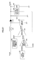
- FIG. 27 is an example of such a switching power supply circuit according to a related art.
- an error amplifying circuit 242 outputs an error voltage EAo 24 obtained by amplifying the difference in voltage between a divided voltage VFB 24 obtained by dividing an output voltage Vout 24 at a voltage dividing resistor 246 and a reference voltage VREF 24 output from a soft-starting circuit 241 .
- a comparator 244 compares a triangular wave signal TW 24 output from a triangular wave generating circuit 243 with the error voltage EAo 24 , and generates and outputs a switching pulse signal Spa 24 for carrying out PWM control to a switch circuit 245 .
- soft-starting circuits such as the aforementioned soft-starting circuit 241
- soft-starting circuit 241 are generally configured to include a capacitor and a resistor; however, in a case where the capacitor is installed in a chip, since the size of the capacitor is large, areas of the capacitor may be too large to be installed in the chip. Moreover, in a case where the capacitor is installed outside, since the number of nodes is increased, the number of components will be increased.
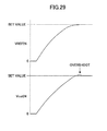
- FIG. 29 there is disclosed a method of applying the reference voltage VREF 24 in a gradual changing manner such that the output voltage Vout 24 is output in a gradual changing manner. Accordingly, the overshoot can be reduced when ramping up the reference voltage VREF 24 .
- embodiments of the present invention may provide a novel and useful switching power supply circuit solving one or more of the problems discussed above. More specifically, the embodiments of the present invention may provide a switching power supply circuit capable of reducing noises that occur during soft-starting operation.
- the “soft-starting operation” used herein is defined as an operation in which a reference voltage is applied in a gradual changing manner such that an output voltage is output in a gradual changing manner during start-up of the switching power supply circuit.
- One aspect of the present invention may be to provide a switching power supply circuit for generating an output voltage at an output node based on an input voltage at an input node that includes a reference voltage generating circuit configured to generate a reference voltage such that during an initial start-up period in which the reference voltage rises from zero voltage to a predetermined voltage a voltage rise rate of the reference voltage within a first predetermined period from a start point of the initial start-up period and a voltage rise rate of the reference voltage within a second predetermined period immediately preceding an end point of the initial start-up period are smaller than a voltage rise rate of the reference voltage in a period between the first predetermined period and the second predetermined period, a coil disposed between the input node and the output node, and a switch circuit configured to switch on and off to control a current running through the coil in response to comparison between the reference voltage and a voltage proportional to the output voltage.
- a reference voltage generating circuit configured to generate a reference voltage such that during an initial start-up period in which the reference voltage rises from
- the reference voltage generating circuit raises the reference voltage such that the voltage rise waveform forms a sine wave.
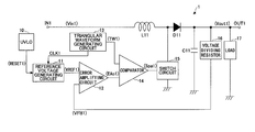
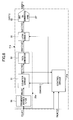
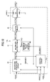
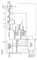
- FIG. 1 is a diagram illustrating a circuit example of a switching power supply circuit according to a first embodiment of the invention.
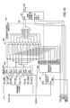
- FIG. 2 is a block diagram illustrating a circuit configuration example of a reference voltage generating circuit 11 in FIG. 1 .
- FIG. 3 is a diagram illustrating a circuit example of a waveform generating circuit 20 in FIG. 2 .
- FIG. 4 is a timing chart illustrating an operational example of the waveform generating circuit 20 in FIG. 3 .
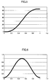
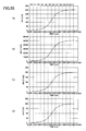
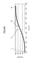
- FIG. 5 is a graph illustrating a waveform example of reference voltage VFRF 1 .
- FIG. 6 is a graph illustrating a waveform example of current flowing into a capacitor C 11 .
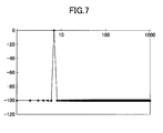
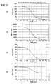
- FIG. 7 is a spectrum waveform diagram illustrating an example of harmonic noises.
- FIG. 8 is a block diagram illustrating a circuit configuration example of a waveform generating circuit in a switching power supply circuit according to a second embodiment of the invention.
- FIG. 9 includes graphs (a) and (b) each illustrating a waveform generation example of reference voltage VREF 1 according to an expression of trigonometric functions.
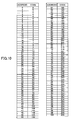
- FIG. 10 is an example of waveform tables.
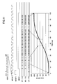
- FIG. 11 is a timing chart illustrating an operational example of a reference voltage generating circuit 11 a in FIG. 8 .
- FIG. 12 is a block diagram illustrating a circuit configuration example of a switching power supply circuit according to a third embodiment of the invention.
- FIG. 13 is a diagram illustrating an operational example of a reference voltage generating circuit 11 b in FIG. 12 .
- FIG. 14 is a diagram illustrating another operational example of a reference voltage generating circuit 11 b in FIG. 12 .
- FIG. 15 is a block diagram illustrating a circuit configuration example of a switching power supply circuit according to a third embodiment of the invention.
- FIG. 16 is a timing chart illustrating an operational example of a reference voltage generating circuit 11 b in FIG. 15 .
- FIG. 17 is a timing chart illustrating another operational example of the reference voltage generating circuit 11 b in FIG. 15 .
- FIG. 18 is a block diagram illustrating a circuit configuration example of a switching power supply circuit according to a fourth embodiment of the invention.
- FIG. 19 is a diagram illustrating a circuit example of a waveform generating circuit 20 c in FIG. 18 .
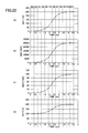
- FIG. 20 includes graphs (a) to (d) each illustrating an operational example of the reference voltage generating circuit 11 c in FIG. 18 .
- FIG. 21 includes graphs (a) to (d) each illustrating another operational example of the reference voltage generating circuit 11 c in FIG. 18 .
- FIG. 22 includes graphs (a) to (d) each illustrating another operational example of the reference voltage generating circuit 11 c in FIG. 18 .
- FIG. 23 is a block diagram illustrating a circuit configuration example of a switching power supply circuit according to a fourth embodiment of the invention.
- FIGS. 24A , 24 B are timing charts illustrating an operational example of a reference voltage generating circuit 11 c in FIG. 23 .
- FIGS. 25A , 25 B are timing charts illustrating another operational example of the reference voltage generating circuit 11 c in FIG. 23 .
- FIGS. 26A , 26 B are timing charts illustrating another operational example of the reference voltage generating circuit 11 c in FIG. 23 .
- FIG. 27 is an example of a switching power supply circuit according to a related art.
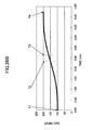
- FIG. 28 is a diagram illustrating examples of reference voltage VREF and output voltage Vout 24 .
- FIG. 29 is a diagram illustrating other examples of reference voltage VREF and output voltage Vout 24 .
- FIG. 30 is a graph illustrating inrush current flowing into a capacitor C 241 in FIG. 27 .
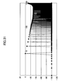
- FIG. 31 is a spectrum waveform diagram illustrating an example of harmonic noises according to the related art.
- FIG. 1 is a diagram illustrating a circuit example of a switching power supply circuit according to a first embodiment of the invention.
- a switching power supply circuit 1 in FIG. 1 increases an output voltage Vout 1 based on an input voltage Vin 1 input to an input node IN 1 to a predetermined voltage and outputs the increased output voltage Vout 1 from an output node OUT 1 .
- the switching power supply circuit 1 also functions as an asynchronous rectifying type raising switching regulator to output the voltage Vout 1 to a load 17 connected to the output node OUT 1 .
- the switching power supply circuit 1 includes a low power supply voltage malfunction preventing circuit (hereinafter, called as “UVLO”) 10 , a reference voltage generating circuit 11 generating and outputting a predetermined reference voltage VREF 1 , an error amplifying circuit 12 , a triangular wave generating circuit 13 generating a predetermined clock signal CLK 1 and a predetermined triangular wave signal TW 1 , and a comparator 14 .
- UVLO low power supply voltage malfunction preventing circuit
- the switching power supply circuit 1 further includes a switch circuit 15 performing switching operation to control an output voltage converted from the input voltage Vin 1 , a voltage dividing resistor 16 dividing the output voltage Vout 1 , and generating and outputting a divided voltage VFB 1 , a rectifying diode D 11 , a coil L 11 , and a capacitor C 11 for obtaining gradual current flow.
- the coil L 11 is connected between the input voltage Vin 1 and an anode of the rectifying diode D 11 , and the switch circuit 15 is connected between the anode of the rectifying diode D 11 and a ground voltage.
- a cathode of the rectifying diode D 11 is connected to the output node OUT 1 .
- the capacitor C 11 is connected between the output node OUT 1 and the ground voltage, and the load 17 is connected likewise between the output node OUT 1 and the ground voltage.
- a reset signal RESET 1 output from UVLO 10 controls the operation of the reference voltage generating circuit 11 , to which the clock signal CLK 1 generated as a reference pulse signal is input, from the triangular wave generating circuit 13 .
- the error amplifying circuit 12 amplifies the difference in voltage between the divided voltage VFB 1 and the reference voltage VREF 1 , and generates and outputs an error voltage EAo 1 .
- the comparator 14 compares voltages between the error voltage EAo 1 and the triangular wave signal TW 1 , generates a pulse signal Spa 1 for performing PWM control based on the comparison outcome, and outputs the pulse signal Spa 1 to the switch circuit 15 .
- the switch circuit 15 is turned ON or OFF based on the pulse signal Spa 1 output from the comparator 14 .
- the switch circuit 15 is conductive when the switch circuit 15 is turned ON whereas the switch circuit 15 is nonconductive when the switch circuit 15 is turned OFF.
- the reference voltage generating circuit 11 starts operating and increases the reference voltage VREF 1 .
- the error voltage EAo 1 from the error amplifying circuit 12 rises, thereby causing the pulse width of the pulse signal Spa 1 from the comparator 14 to change.
- the amount of time in which the switch circuit 15 is turned ON gets longer, thereby increasing the output voltage Vout 1 .
- the divided voltage VFB 1 becomes equal to the reference voltage VREF 1 , and the reference voltage VREF 1 rises to a set value, thereby controlling the output voltage Vout 1 to be a predetermined voltage.
- the switching power supply circuit 1 repeats the aforementioned operation so as to control the output voltage Vout 1 so as to maintain at a constant voltage.
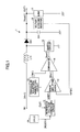
- FIG. 2 is a block diagram illustrating a circuit configuration example of a reference voltage generating circuit 11 in FIG. 1 .
- the reference voltage generating circuit 11 includes a waveform generating circuit 20 determining an output waveform data, a control circuit 21 controlling operation of the waveform generating circuit 20 after the reset cancellation, a latch circuit 22 maintaining the waveform data output from the waveform generating circuit 20 , and a DA converter 23 converting digital data output from the latch circuit 22 into an analog signal and outputting the analog signal.
- the waveform generating circuit 20 , the latch circuit 22 and the DA converter 23 , and the control circuit 21 respectively form a waveform generating circuit section, a DA converter section, and a control circuit section.
- the reset signal RESET 1 output from UVLO 10 is input to the waveform generating circuit 20 and the control circuit 21 whereas the clock signal CLK 1 output from the triangular wave generating circuit 13 is input to the waveform generating circuit 20 and the control circuit 21 .
- the waveform generating circuit 20 and the control circuit 21 are synchronized by using the clock signal CLK 1 .
- a control signal SMODE 1 output from the control circuit 21 is input to the waveform generating circuit 20 and the latch circuit 22
- a waveform data SO 1 [7:0] of 8-bit digital data output from the waveform generating circuit 20 is input to the control circuit 21 and the latch circuit 22 .
- a digital data LO 1 [7:0] output from the latch circuit 22 is converted into the reference voltage VREF 1 of an analog signal to be output by the DA converter 23 .
- the DA converter 23 is supplied with a predetermined reference voltage VRT 1 for use in DA conversion.
- the control circuit 21 sets the control signal SMODE 1 at a high level to initiate a soft-starting operation when the reset signal RESET 1 is switched to a low level, and the waveform generating circuit 20 initiates data change of the waveform data SO 1 [7:0].
- the waveform generating circuit 20 changes the waveform data SO 1 [7:0] for generating a gradual waveform by changing a count clock as the time elapses.
- the control circuit 21 sets the control signal SMODE 1 at the low level to stop the operation of the waveform generating circuit 20 , thereby terminating the soft-starting operation.
- the latch circuit 22 outputs the waveform data SO 1 [7:0] as the digital data LO 1 [7:0] without any change while the control signal SMODE 1 stays at the high level.
- the latch circuit 22 maintains the waveform data SO 1 [7:0] input when the control signal SMODE 1 is switched to the low level and outputs the maintained waveform data SO 1 [7:0] as the digital data LO 1 [7:0].
- the digital data LO 1 [7:0] from the latch circuit 22 is converted from digital to analog at the DA converter 23 and the converted data is output as the reference voltage VREF 1 .
- the latch circuit 22 may be omitted such that the waveform data SO 1 [7:0] output from the waveform generating circuit 20 is directly input to the DA converter 23 .
- the waveform generating circuit 20 is configured to maintain the waveform data SO 1 [7:0] output when the control signal SMODE 1 is switched to the low level, and output the maintained waveform data SO 1 [7:0].
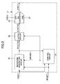
- FIG. 3 is a diagram illustrating a circuit example of a waveform generating circuit 20 in FIG. 2 .
- the waveform generating circuit 20 includes a counter circuit 31 counting the clock signal CLK 1 to increment by one count for every 1024 clocks, a frequency divider 32 generating and outputting frequency divided clock signals S(1/16), S(1/32), S(1/64), S(1/128) and S(1/256) obtained by dividing the frequency of the clock signal CLK 1 by 16, 32, 64, 128 and 256, and a decoder circuit 33 generating and outputting selection signals S 0 to S 11 for selecting the frequency divided clock signals output from the frequency divider 32 based on the signal output from the counter circuit 31 .
- the waveform generating circuit 20 includes a combinational circuit 34 combining the selection signals S 0 to S 11 output from the decoder circuit 33 with the frequency divided clock signals S1/16), S(1/32), S(1/64), S(1/128) and S(1/256) output from the frequency divider 32 using AND circuits and an OR circuit, an AND circuit 35 outputting a signal output from the combinational circuit 34 provided that the control signal SMODE 1 is at a high level, and a code counter circuit 36 counting the number of pulses of a signal output from the AND circuit 35 , converting the signal into 8-bit waveform data SO 1 [7:0], and outputting the converted 8-bit waveform data.
- the counter circuit 31 , the frequency divider 32 , the decoder circuit 33 , the combinational circuit 34 and the AND circuit 35 , and the code counter circuit 36 respectively form a counter circuit section, a frequency dividing section, a selection circuit section, a combinational circuit section, and code counter circuit section.
- the counter circuit 31 defines a length of one interval by outputting the 4-bit digital data to the decoder 33 .
- the decoder circuit 33 receives the digital data from the counter circuit 31 and outputs the selection signals S 0 to S 11 each indicating one of 12 intervals, and determines a cycle of data change for each interval by selecting the frequency divided clock signals S(1/16), S(1/32), S(1/64), S(1/128) and S(1/256) at the combinational circuit 34 .
- the waveform generating circuit 20 further includes the AND circuit 35 such that the signal output from the combinational circuit 34 is output to the code counter circuit 36 provided that the control signal SMODE 1 is at the high level.
- the code counter 36 counts the number of pulses of the signal output from the AND circuit 35 , and generates and outputs the 8-bit waveform data SO 1 [7:0].
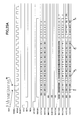
- FIG. 4 is a timing chart illustrating waveform examples of the signals in FIG. 3 , and a more detailed operation of the waveform generating circuit 20 in FIG. 3 will be described with reference to FIG. 4 .
- One interval is indicated by an interval between vertical dotted lines in FIG. 4 , the dotted lines each correspond to the 1024 th clock of the clock signal CLK 1 .
- the counter circuit 31 starts counting.
- the decoder circuit 33 sets the selection signal S 0 at the low level and the selection signal S 1 at the high level.
- the decoder circuit 33 repeats this operation from the selection signals S 0 to S 11 .
- the combinational circuit 34 determines a cycle of code count for each interval, and the code counter circuit 36 increments by one count based on the cycle. In the interval where the selection signal S 0 stays at the high level, the code counter circuit 36 increments by one count for every 256 clocks, and increments four counts before the selection signal S 0 is switched to the low level.
- FIG. 4 shows the frequency divided clock signals selected in the corresponding intervals and values counted by the code counter circuit 36 based on the frequency divided clock signals.
- the count cycles of the code counter circuit 36 in the intervals are changed by selecting one of the frequency divided clock signals of the corresponding interval, thereby changing the slope of the data waveform output from the code counter circuit 36 .
- the 8-bit waveform data SO 1 [7:0] output from the code counter circuit 36 is converted from digital to analog data by the DA converter 23 in FIG. 2 and generated as the reference voltage VREF 1 exhibiting the waveform shown in FIG. 5 .
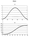
- the reference voltage VREF 1 that gradually rises to form a sine wave is generated such that during an initial start-up period in which the reference voltage rises from zero voltage to a predetermined voltage, degrees of a slope K 1 of the reference voltage VREF 1 within a first predetermined period from a start point of the initial start-up period and degrees of a slope K 3 of the reference voltage VREF 1 within a second predetermined period immediately preceding an end point of the initial start-up period are smaller than degrees of a slope K 2 of the reference voltage VREF 1 in a period between the first predetermined period and the second predetermined period.
- a counting system by the counter circuit 31 frequencies divided by the frequency divider 32 , the number of intervals determined by the decoder circuit 33 , combinations determined by the combinational circuit 34 , the number of bits output by the code counter circuit 36 , and the like can optionally be changed and adjusted.
- the switching power supply circuit according to the first embodiment is configured such that the reference voltage VREF 1 after turning on the power supply includes the waveform shown in FIG. 5 , the noises that occur during the soft-starting operation can be reduced to a large extent.
- the switching power supply circuit according to the first embodiment since the output voltage after turning on the power supply can gradually rise up without largely consuming the capacitance, the overshoot that occurs during the output voltage start-up can be reduced.
- the value of the reference voltage VREF 1 or the set voltage of the output voltage Vout 1 can be changed by changing the predetermined reference voltage VRT 1 of the DA converter 23 in FIG.
- FIG. 8 is a block diagram illustrating a circuit configuration example of a switching power supply circuit according to a second embodiment of the invention. Note that a diagram illustrating the circuit configuration example of the switching power supply circuit according to the second embodiment is identical to that in FIG. 1 except that the reference numeral 11 given to the reference voltage generating circuit in FIG. 1 is 11 a , and illustration thereof is thus omitted.
- FIG. 8 components either identical or similar to those in FIG. 2 are given by the same reference numerals, and descriptions thereof are thus omitted. Only the configuration differing from that in FIG. 2 will be described below.
- the waveform generating circuit 20 in FIG. 2 is configured to include a frequency divider 50 , a counter circuit 51 and a data converter 52 .
- the reference voltage generating circuit 11 and the waveform generating circuit 20 in FIG. 2 respectively correspond to a reference voltage generating circuit 11 a and a waveform generating circuit 20 a in FIG. B.
- the reference voltage generating circuit 11 a includes the waveform generating circuit 20 a determining an output waveform data, the control circuit 21 controlling operation of the waveform generating circuit 20 a after the reset cancellation, the latch circuit 22 maintaining the waveform data output from the waveform generating circuit 20 a , and the DA converter 23 converting digital data output from the latch circuit 22 into an analog signal and outputting the analog signal.
- the waveform generating circuit 20 a includes the frequency divider 50 dividing the frequency of the clock signal CLK 1 output from the triangular wave generating circuit 13 , the counter circuit 51 counting the number of pulses of a frequency divided clock signal MCLK 1 output from the frequency divider 50 and outputting count data CT 1 [7:0] indicating the counted value, and the data converter 52 converting the count data CT 1 [7:0] output from the counter circuit 51 into waveform data SO 1 [7:0] by a predetermined method and outputting the converted data.
- the frequency divider 50 , the counter circuit 51 , and the data converter 52 respectively form a frequency dividing section, a counter circuit section, and a data converter section.
- the reset signal RESET 1 output from UVLO 10 is input to the control circuit 21
- the clock signal CLK 1 from the triangular wave generating circuit 13 is input to the frequency divider 50 and the control circuit 21 .
- the control signal SMODE 1 output from the control circuit 21 is input to the counter circuit 51 and latch circuit 22
- the frequency divided clock signal MCLK 1 output from the frequency divider 50 is input to the counter circuit 51 .
- the B-bit count data CT 1 [7:0] output from the counter 51 is input to the data converter 52
- 8-bit waveform data SO 1 [7:0] output from the data converter 52 is input to the latch circuit 22 .
- the data converter 52 that determines which waveform data SO 1 [7:0] is output based on the count data CT 1 [7:0] will be described below.
- the data converter 52 generates the waveform data SO 1 [7:0] based on the expression of trigonometric functions as shown in FIG. 9 .
- FIG. 9 each illustrate a one-cycle sine wave as one example.
- the values of the sine wave in FIG. 9( a ) that are progressively added result in a waveform shown in FIG. 9( b ), whereby the waveform is used for a rise waveform.
- the horizontal axis indicates addresses including 0 to 100 whereas the vertical axis indicates codes including a maximum of eight bits.
- FIG. 10 is an example of the waveform table including the addresses and codes; however, address numbers and number of bits for the codes given in the waveform table are only an example and are not limited thereto. Any address numbers and any number of bits for the codes can optionally be set.
- FIG. 11 is a timing chart illustrating examples of the signals in FIG. 8 , and operation of the reference voltage generating circuit 11 a in FIG. 8 will be described with reference to FIG. 11 .
- the frequency divider 50 divides the frequency of the clock signal CLK 1 output from the triangular wave generating circuit 13 by 128 , and generates and outputs the frequency divided clock signals MCLK 1 .
- the control signal SMODE 1 is switched to a high level, thereby initiating soft-starting operation.
- the counter circuit 51 starts counting the number of pulses of input frequency divided clock signals MCLK 1 and outputs 8-bit count data CT 1 [7:0] indicating the counted value.
- the data converter 52 generates and outputs the waveform data SO 1 [7:0] using the waveform table shown in FIG. 10 . Specifically, the data converter 52 uses the count data CT 1 [7:0] as an address in FIG. 10 , and outputs a code corresponding to the address as 8-bit waveform data SO 1 [7:0]. If the address of the count data CT 1 [7:0] obtains a predetermined data, such as 100 , the control circuit 21 switches the control signal SMODE 1 to the low level, thereby terminating the soft-starting operation.
- the latch circuit 22 When the soft-starting operation is terminated, the latch circuit 22 outputs the waveform data SO 1 [7:0] as the digital data LO 1 [7:0] without any change while the control signal SMODE 1 stays at the high level. By contrast, the latch circuit 22 maintains the waveform data SO 1 [7:0] input when the control signal SMODE 1 is switched to the low level and outputs the maintained waveform data SO 1 [7:0] as the digital data LO 1 [7:0].
- the digital data LO 1 [7:0] is input to the DA converter 23 , which converts input digital data LO 1 [7:0] into analog data and outputs the analog data as the reference voltage VREF 1 .
- the reference voltage generating circuit 11 a in FIG. 8 is only one example, and the latch circuit 22 may be omitted such that the waveform data SO 1 [7:0] output from the data converter 52 is directly input to the DA converter 23 .
- the counter circuit 51 is configured such that the counter circuit 51 maintains and outputs the counted data output when the control signal SMODE 1 is switched to the low level.
- the switching power supply circuit according to the second embodiment exhibits similar effectiveness as that of the first embodiment, and the rise time of the reference voltage VREF 1 can be adjusted by adjusting the frequency dividing ratio of the frequency divider 50 .
- FIG. 12 is a block diagram illustrating a circuit configuration example of a switching power supply circuit according to a third embodiment of the invention.
- FIG. 12 a diagram illustrating the circuit configuration example of the switching power supply circuit according to the third embodiment is identical to that in FIG. 1 except that the reference numeral 11 given to the reference voltage generating circuit in FIG. 1 is 11 b , and illustration thereof is thus omitted.
- FIG. 12 components either identical or similar to those in FIG. 2 are given by the same reference numerals, and descriptions thereof are thus omitted. Only the configuration differing from that in FIG. 2 will be described below.
- FIG. 12 The configuration difference between FIG. 12 and FIG. 2 is as follows.
- the control circuit 21 in FIG. 2 corresponds to a control circuit 21 b , and a multiplier 91 and a maximum output code register 92 are added thereto.
- the reference voltage generating circuit 11 in FIG. 2 corresponds to the reference voltage circuit 11 b in FIG. 12 .
- the reference voltage generating circuit 11 b includes a waveform generating circuit 20 , the control circuit 21 b controlling operation of the waveform generating circuit 20 after reset cancellation, the multiplier 91 , the maximum output code register 92 , a latch circuit 22 maintaining data output from the multiplier 91 , and a DA converter 23 .
- the control circuit 21 b , the multiplier 91 , and the maximum output code register 92 respectively form a control circuit section, a multiplier section, and a maximum output code storage section.
- the control circuit 21 b outputs the control signal SMODE 1 based on the clock signal CLK 1 output from the triangular waveform generating circuit 13 and the reset signal RESET 1 , and outputs a maximum output code setting signal SELMAX 1 to the maximum output code register 92 based on a signal VSEL 1 input from outside.
- the multiplier 91 multiplies the waveform data SO 1 [7:0] output from the waveform generating circuit 20 by the maximum output code MAX 1 [7:0] input from the maximum output code register 92 , and outputs the digital data MO 1 [15:8] formed of the higher-order 8 bit data indicating the multiplied outcome.
- the latch circuit 22 outputs the input digital data MO 1 [15:8] as the digital data LO 1 [7:0] without any change while the control signal SMODE 1 stays at the high level. By contrast, the latch circuit 22 maintains the digital data MO 1 [15:8] input when the control signal SMODE 1 is switched to the low level and outputs the maintained digital data MO 1 [15:8] as the digital data LO 1 [7:0].
- the control circuit 21 b switches the control signal SMODE 1 to the high level to initiate the soft-starting operation, and the waveform generating circuit 20 starts operating.
- the control circuit 21 b switches the control signal SMODE 1 to the low level, thereby initiating the soft-starting operation.
- the control circuit 21 b outputs the maximum output code setting signal SELMAX 1 to the maximum output code register 92 based on the input signal VSEL 1 .
- the control circuit 21 b outputs the signal SELMAX 1 to the maximum output code register 92 such that the maximum output code MAX 1 [7:0] indicates 100 when the signal VSEL 1 is switched to the low level whereas the maximum output code MAX 1 [7:0] indicates 200 when the signal VSEL 1 is switched to the high level.
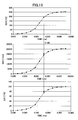
- FIG. 13 illustrates the digital data MO 1 [15:8] and LO 1 [7:0] corresponding to the waveform data SO 1 [7:0] when the signal VSEL 1 is switched to the low level
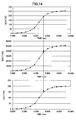
- FIG. 14 illustrates the digital data MO 1 [15:8] and LO 1 [7:0] corresponding to the waveform data SO 1 [7:0] when the signal VSEL 1 is switched to the high level.
- FIG. 12 only illustrates an example where the multiplier 91 and the maximum output code register 92 are provided in the circuit configuration of FIG. 2 ; however, the example may also be configured such that the multiplier 91 and the maximum output code register 92 may be provided in the circuit configuration of FIG. 8 , as shown in FIG. 15 .
- FIG. 15 components either identical or similar to those in FIG. 12 are given by the same reference numerals, and descriptions thereof are thus omitted. Only the configuration differing from that in FIG. 12 will be described below.
- the reference voltage generating circuit 11 b includes a waveform generating circuit 20 a , the control circuit 21 b controlling operation of the waveform generating circuit 20 a after reset cancellation, the multiplier 91 , the maximum output code register 92 , the latch circuit 22 maintaining data output from the multiplier 91 , and the DA converter 23 converting the data output from the latch circuit 22 into an analog data.
- the control circuit 21 b outputs the control signal SMODE 1 based on the clock signal CLK 1 output from the triangular waveform generating circuit 13 and the reset signal RESET 1 , and outputs a maximum output code setting signal SELMAX 1 to the maximum output code register 92 based on a signal VSEL 1 input from outside.
- the multiplier 91 multiplies the waveform data SO 1 [7:0] output from the waveform generating circuit 20 a by the maximum output code MAX 1 [7:0] input from the maximum output code register 92 , and outputs the digital data MO 1 [15:8] indicating the higher-order 8 bit data indicating the multiplied outcome.
- the latch circuit 22 outputs the input digital data MO 1 [15:8] as the digital data LOT [7:0] without any change while the control signal SMODE 1 stays at the high level. By contrast, the latch circuit 22 maintains the digital data MO 1 [15:8] input when the control signal SMODE 1 is switched to the low level and outputs the maintained digital data MO 1 [15:8] as the digital data LO 1 [7:0].
- FIG. 16 is a timing chart illustrating the signals in FIG. 15 when the signal VSEL 1 is switched to the low level
- FIG. 17 is a timing chart illustrating the signals in FIG. 15 when the signal VSEL 1 is switched to the high level.
- the multiplier 91 multiplies the waveform data SO 1 [7:0] by 100 to obtain 16-bit digital data MO 1 [15:0] as the multiplied outcome, and outputs the digital data MO 1 [15:8] indicating the higher-order 8 bit data.
- the latch circuit 22 outputs the digital data MO 1 [15:8] as the digital data LOT [7:0] without any change while the control signal SMODE 1 stays at the high level.
- the latch circuit 22 maintains the digital data MO 1 [15:8] input when the control signal SMODE 1 is switched to the low level and outputs the maintained digital data MO 1 [15:8] as the digital data LO 1 [7:0].
- the digital data LO 1 [7:0] is converted from digital to analog data at the DA converter 23 and the converted data is output as the reference voltage VREF 1 .
- the reference voltage generating circuit 11 b performs operation similar to that shown in FIG. 17 when the signal VSEL 1 is switched to the high level.
- circuit configuration illustrated in FIGS. 12 and 15 is only one example, in which two types of data 100 and 200 are stored in the maximum output code register 92 ; however, the circuit may be configured such that the data may optionally be input to the maximum output code register 92 from outside.
- the switching power supply circuit according to the third embodiment exhibits similar effectiveness as that of the first embodiment, and since the maximum output code can be set thereto, the value of the reference voltage VREF 1 , that is, the set value of the output voltage Vout 1 can be changed.
- FIG. 18 is a block diagram illustrating a circuit configuration example of a switching power supply circuit according to a fourth embodiment of the invention.
- FIG. 18 a diagram illustrating the circuit configuration example of the switching power supply circuit according to the fourth embodiment is identical to that in FIG. 1 except that the reference numeral 11 given to the reference voltage generating circuit in FIG. 1 is 11 c , and illustration thereof is thus omitted.
- FIG. 18 components either identical or similar to those in FIG. 12 are given by the same reference numerals, and descriptions thereof are thus omitted. Only the configuration differing from that in FIG. 12 will be described below.
- FIG. 18 The configuration difference between FIG. 18 and FIG. 12 is as follows.
- the waveform generating circuit 20 and the control circuit 21 b in FIG. 12 respectively correspond to a waveform generating circuit 20 c and a control circuit 21 c , and a minimum output code register 93 , a subtracter 94 and an adder 95 are added thereto.
- the reference voltage generating circuit 11 b in FIG. 12 corresponds to the reference voltage circuit 11 c in FIG. 18 .
- the reference voltage generating circuit 11 c includes the waveform generating circuit 20 c , the control circuit 21 c , the multiplier 91 , the maximum output code register 92 , the minimum output code register 93 , the subtracter 94 , the adder 95 , the latch circuit 22 , and the DA converter 23 .
- the waveform generating circuit 20 c , the control circuit 21 c , the minimum output code register 93 , the subtracter 94 , and the adder 95 respectively form a waveform generating circuit section, a control circuit section, a minimum output code storage section, a subtracter section, and an adder section.
- the control circuit 21 c outputs the control signal SMODE 1 to the waveform generating circuit 20 c and the latch circuit 22 based on the clock signal CLK 1 output from the triangular waveform generating circuit 13 and the reset signal RESET 1 output from the UVLO 10 .
- the control circuit 21 c outputs the maximum output code setting signal SELMAX 1 to the maximum output code register 92 while simultaneously outputting the minimum output code setting signal SELMIN 1 to the minimum output code register 93 , based on the externally input signal VSEL 1 . Further, the control circuit 21 c receives a signal H/L 1 from outside, and controls to initiate operation, set, increment and decrement counts of the waveform generating circuit 20 c.
- the waveform generating circuit 20 c which is controlled by the clock signal CLK 1 and the control circuit 21 c , generates and outputs the waveform data SO 1 [7:0].
- the subtracter 94 subtracts the minimum output code MIN 1 [7:0] output from the minimum output code register 93 from the maximum output code MAX 1 [7:0] output from the maximum output code register 92 , and generates and outputs a digital data DO 1 [7:0].
- the multiplier 91 multiplies the waveform data SO 1 [7:0] output from the waveform generating circuit 20 c by the digital data DO 1 [7:0] input from the subtracter 94 , and outputs the digital data MO 1 [15:8] formed of the higher-order 8 bit data indicating the multiplied outcome.
- the adder 95 adds the digital data MO 1 [15:8] output from the multiplier 91 and the minimum output code MIN 1 [7:0] output from the minimum output register 94 , and generates and outputs an 8-bit digital data AO 1 [7:0].
- the latch circuit 22 outputs the input digital data AO 1 [7:0] as the digital data LO 1 [7:0] without any change while the control signal SMODE 1 stays at the high level, and maintains the digital data AO 1 [7:0] input when the control signal SMODE 1 is switched to the low level and outputs the maintained digital data AO 1 [7:0] as the digital data LO 1 [7:0].
- the digital data LO 1 [7:0] output from the latch circuit 22 is converted from digital to analog data at the DA converter 23 and the converted data is output as the reference voltage VREF 1 .
- the latch circuit 22 may be omitted such that the digital data AO 1 [7:0] output from the adder 95 is directly input to the DA converter 23 .
- the waveform generating circuit 20 c is configured to maintain the waveform data SO 1 [7:0] output when the control signal SMODE 1 is switched to the low level, and output the maintained waveform data SO 1 [7:0].
- FIG. 19 is a diagram illustrating a circuit example of a waveform generating circuit 20 c in FIG. 18 .
- the waveform generating circuit 20 c includes a frequency divider 101 generating and outputting frequency divided clock signals S(1/8), S(1/16), S(1/32), S(1/64), S(1/128), S(1/256), S(1/512), and S(1/1024) obtained by dividing the frequency of the clock signal CLK 1 by 8, 16, 32, 64, 128, 256, 512, and 1024, and a selector 102 selecting combinations between the frequency divided clock signals S(1/8), S(1/16), S(1/32), S(1/64), S(1/128), S(1/256), S(1/512), and S(1/1024) based on the signal CKSEL 1 input from the control circuit 21 c.
- the waveform generating circuit 20 c further includes a counter circuit 103 counting the number of clock pulses of the frequency divided clock signal S(1/512) or (1/1024) selected based on the signal CKSEL 1 , a decoder circuit 104 generates and outputs selection signals S 0 to S 11 for selecting the frequency divided signals output from the selector 102 based on the signal output from the counter circuit 103 , a combinational circuit 104 combining the selection signals S 0 to S 11 output from the decoder circuit 104 with the frequency divided clock signals output from the selector 102 using AND circuits and an OR circuit, an AND circuit 106 outputting a signal output from the combinational circuit 105 provided that the control signal SMODE 1 is at a high level, and a code counter circuit 107 counting the number of pulses of the signal output from the AND circuit 106 , converting the signal into the 8-bit waveform data SO 1 [7:0], and outputting the converted 8-bit waveform data.
- the counter circuit 101 the frequency divider 102 , the decoder circuit 104 , the combinational circuit 105 and the AND circuit 106 , and the code counter circuit 107 respectively form a counter circuit section, a frequency dividing section, a selection circuit section, a combinational circuit section, and a code counter circuit section.
- a rising edge of the reset signal RESET 1 at the high level triggers the signal CKSEL 1 , a signal RES 1 , and an up-down signal UP/DN 1 to switch to the high level.
- the selector 102 selects and outputs the frequency divided signal S(1/1024) when the signal CKSEL 1 is at the high level, and selects and outputs the frequency divided signal S(1/512) when the signal CKSEL 1 is at the low level.
- the code counter circuit 107 is reset when the signal RES 1 is at the high level.
- the code counter circuit 107 increments counts when the up-down signal UP/DN 1 is at the high level and decrements counts when the up-down signal UP/DN 1 is at the low level.
- the control circuit 21 c switches the control signal SMODE 1 to the high level when the reset signal RES 1 is switched to the low level, thereby initiating soft-starting operation and operation of the waveform generating circuit 21 c .
- the counter circuit 103 counts the clock signal CLK 1 to increment by one count for every 1024 clocks and outputs 4-bit digital data indicating the counted value to the decoder circuit 104 .
- the decoder circuit 104 outputs the signal indicating 12 intervals of the selection signals S 0 to S 11 based on the digital data input from the counter 103 , and count cycles for the corresponding intervals are determined based on the frequency divided clock signals output from the selector 102 .
- the code counter circuit 107 increments by one count: by 1/256 cycle when the selection signal S 0 is switched to the high level; by 1/256 cycle when the selection signal S 1 is switched to the high level; by 1/128 cycle when the selection signal S 2 is switched to the high level; by 1/64 cycle when the selection signal S 3 is switched to the high level; by 1/32 cycle when the selection signal S 4 is switched to the high level; by 1/16 cycle when the selection signal S 5 is switched to the high level; by 1/16 cycle when the selection signal S 6 is switched to the high level; by 1/32 cycle when the selection signal S 7 is switched to the high level; by 1/64 cycle when the selection signal S 8 is switched to the high level; by 1/128 cycle when the selection signal S 9 is switched to the high level; by 1/256 cycle when the selection signal S 10 is switched to the high level; and by 1/256 cycle when the selection signal S 11 is switched to the high level.
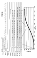
- FIG. 20 includes graphs (a) to (d) each illustrating an operational example of the reference voltage generating circuit 11 c when the signal VSEL 1 is at the high level.
- the code counter circuit 107 performs count-up operation when the up-down signal UP/DN 1 is switched to the high level, and outputs 8-bit waveform data SO 1 [7:0] indicating the counted value as shown in FIG. 20( a ).
- the maximum output code of the maximum output code register 92 is set at 200 and the minimum output code of the minimum output coed register 93 is set at 100 when the signal VSEL 1 output from the control circuit 21 c is switched to the high level.
- the maximum output code of the maximum output code register 92 is set at 200 and the minimum output code of the minimum output coed register 93 is set at 100 when the signal VSEL 1 output from the control circuit 21 c is switched to the low level. Note that the minimum output code of the minimum code register 93 is set at 0 during the soft-starting operation, regardless of the levels of the signal VSEL 1 .
- the maximum output code MAX 1 [7:0] indicates 200 when the signal VSEL 1 is at the high level, and the minimum output code MIN 1 [7:0] indicates 0 during the soft-starting operation.
- the subtracter 94 subtracts the minimum output code MIN 1 [7:0] from the maximum output code MAX 1 [7:0], and the digital data DO 1 [7:0] output from the subtracter 94 indicates 200.
- the multiplier 91 multiplies the waveform data SO 1 [7:0] output from the waveform generating circuit 20 c by the digital data DO 1 [7:0] indicating 200 output from the subtracter 94 , thereby obtaining 16-bit digital data MO 1 [15:0] as shown in FIG. 20( b ).
- the adder 95 adds the digital data MO 1 [15:8] output from the multiplier 91 and the minimum output code MIN 1 [7:0] output from the minimum output register 93 , and outputs the digital data AO 1 [7:0] as shown in FIG. 20( d ).
- the latch circuit 22 outputs the digital data AO 1 [7:0] as the digital data LO 1 [7:0] without any change while the control signal SMODE 1 stays at the high level.
- the latch circuit 22 maintains the digital data AO 1 [7:0] input when the control signal SMODE 1 is switched to the low level and outputs the maintained digital data AO 1 [7:0] as the digital data LO 1 [7:0].
- the digital data LO 1 [7:0] is converted from digital to analog data at the DA converter 23 and the converted data is output as the reference voltage VREF 1 .
- the control circuit 21 c switches the control signal SMODE 1 to the low level and terminates the soft-starting operation.
- the signal CKSEK 1 is switched to the low level, and the selector 102 switches the frequency divided clock signal input to the counter circuit 103 from the frequency divided signal S(1/1024) to the frequency divided signal S(1/512).
- the selector 102 also switches the frequency divided clock signal input to the combinational circuit 105 .
- the code counter circuit 107 increments by one count: by 1/128 cycle when the selection signal S 0 is switched to the high level; by 1/128 cycle when the selection signal S 1 is switched to the high level; by 1/64 cycle when the selection signal S 2 is switched to the high level; by 1/32 cycle when the selection signal S 3 is switched to the high level; by 1/16 cycle when the selection signal S 4 is switched to the high level; by 1/8 cycle when the selection signal S 5 is switched to the high level; by 1/8 cycle when the selection signal S 6 is switched to the high level; by 1/16 cycle when the selection signal S 7 is switched to the high level; by 1/32 cycle when the selection signal S 8 is switched to the high level; by 1/64 cycle when the selection signal S 9 is switched to the high level; by 1/128 cycle when the selection signal S 10 is switched to the high level; and by 1/128 cycle when the selection signal S 11 is switched to the high level.
- the minimum output code MIN 1 [7:0] When the minimum output code MIN 1 [7:0] is switched to 100, the digital data DO 1 [7:0] output from the subtracter 94 is switched to 100, the digital data MO 1 [15:0] obtained at the multiplier 91 is switched from 51000 to 25500, and the digital data MO 1 [15:8] is switched from 200 to 100.
- the minimum output code MIN 1 [7:0] indicating 100 is added to the digital data MO 1 [15:8] indicating 100 to give 200 to the digital data AO 1 [7:0] output from the adder 95 , which is an equivalent value after soft-starting operation.
- the latch circuit 22 maintains the digital data AO 1 [7:0] input when the control signal SMODE 1 is at the low level and outputs the maintained digital data AO 1 [7:0] without any change, and the digital data LO 1 [7:0] thus remains unchanged.
- the digital data LO 1 [7:0] gradually rises up from 0 to 200 as shown in FIG. 20( d ).
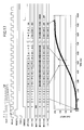
- FIG. 21 includes graphs (a) to (d) each illustrating another operational example of the reference voltage generating circuit 11 c when the signal VSEL 1 is at the high level, and the output voltage Vout 1 is changed after the soft-starting operation has finished.
- the control circuit 21 c switches a signal SET 1 to the high level, the up-down signal UP/DN 1 to the low level, and the control signal SMODE 1 to the high level when the signal H/L 1 from outside is switched from the high level to low level.
- the code counter circuit 107 changes the waveform data SO 1 [7:0] to 255 as shown in FIG. 21( a ) when the signal SET 1 is switched to the high level, and starts decrementing counts based on the signal input from AND circuit 106 when the up-down signal UP/DN 1 is switched to the low level.
- the code counter circuit 107 decrements counts until the waveform data SO 1 [7:0] indicates 0, and the control circuit 21 c switches the control signal SMODE 1 to the low level when the waveform data SO 1 [7:0] indicates 0.
- the multiplier 91 , the maximum output code register 92 , the minimum output code register 93 , the subtracter 91 , the adder 95 , the latch circuit 22 and the DA converter 23 each operate in a similar manner as their operation during the soft starting operation. Accordingly, the digital data LO 1 [7:0] input to the DA converter 23 exhibits a gradual change from 200 to 100 in the same manner as the digital data AO 1 [7:0] as shown in FIG. 21( d ).
- FIG. 22 includes graphs (a) to (d) each illustrating another operational example of the reference voltage generating circuit 11 c when the signal HL 1 is switched from the low level to the high level while the signal VSEL 1 stays at the high level.
- the control circuit 21 c switches the signal RES 1 , the up-down signal UP/DN 1 , and the control signal SMODE 1 to the high level when the signal H/L 1 is switched from the low level to the high level.
- the code counter circuit 107 changes the waveform data SO 1 [7:0] to 0 as shown in FIG. 22( a ) when the signal RES 1 is switched to the high level, and starts incrementing counts based on the signal input from the AND circuit 106 when the up-down signal UP/DN 1 is switched to the high level.
- the code counter circuit 107 increments counts until the waveform data SO 1 [7:0] indicates 255, and the control circuit 21 c switches the control signal SMODE 1 to the low level when the waveform data SO 1 [7:0] indicates 255.
- the multiplier 91 , the maximum output code register 92 , the minimum output code register 93 , the subtracter 91 , the adder 95 , the latch circuit 22 and the DA converter 23 each operate in a similar manner as their operation during the soft-starting operation.
- the digital data LO 1 [7:0] input to the DA converter 23 exhibits a gradual change from 100 to 200 in the same manner as the digital data AO 1 [7:0] as shown in FIG. 21( d ).
- circuit configurations shown in FIGS. 18 and 19 are only one example, and the maximum output code of the maximum output code register 92 and the minimum output code of the minimum output code register 93 , and frequency dividing ratio of the frequency divider 101 may optionally be set.
- FIG. 18 only illustrates an example where the minimum output code register 93 , the subtracter 94 , and the adder 95 are provided in the circuit configuration of FIG. 12 ; however, the example may also be configured such that the minimum output code register 93 , the subtracter 94 , and the adder 95 may be provided in the circuit configuration of FIG. 15 , as shown in FIG. 23 .
- FIG. 23 components either identical or similar to those in FIG. 18 are given by the same reference numerals, and descriptions thereof are thus omitted. Only the configuration differing from that in FIG. 18 will be described below.
- the reference voltage generating circuit 11 c includes the waveform generating circuit 20 c , the control circuit 21 c , the multiplier 91 , the maximum output code register 92 , the minimum output code register 93 , the subtracter 94 , the adder 95 , the latch circuit 22 , and the DA converter 23 .
- the waveform generating circuit 20 c includes the frequency divider 50 c dividing the frequency of the clock signal CLK, the counter circuit 51 c counting the number of pulses of divided clock signal MCLK 1 output from the frequency divider 50 c and outputting count data CT 1 [7:0] indicating the counted value, and the data converter 52 converting the count data CT 1 [7:0] output from the counter circuit 51 c into the waveform data SO 1 [7:0] by a predetermined method and outputting the converted data.
- the frequency divider 50 c and the counter circuit 51 c respectively form the frequency divider section and the counter circuit section.
- the control circuit 21 c outputs the control signal SMODE 1 to the counter circuit 51 c and the latch circuit 22 based on the clock signal CLK 1 output from the triangular waveform generating circuit 13 and the reset signal RESET 1 output from the UVLO 10 .
- the control circuit 21 c that receives the signal H/L 1 from outside controls the frequency divider 50 c to obtain the frequency dividing ratio, the initiation of operation, setting, resetting, and count up and count down for the counter circuit 51 c .
- the frequency divider 50 c divides the input clock signal CLK 1 by any one of the frequency dividing ratios 1/64 and 1/128 based on the signal CKSEL 1 input from the control circuit 21 c , and outputs the frequency divided signal as the frequency divided signal MCLK 1 .
- the counter circuit 51 c counts the number of pulses of the frequency divided clock signal MCLK 1 output from the frequency divider 50 c and outputs the count data CT 1 [7:0] indicating the counted value.
- the data converter 52 converts the count data CT 1 [7:0] output from the counter circuit 51 c into waveform data SO 1 [7:0] and outputs the converted data to the multiplier 91 .
- FIGS. 24A , 24 B are timing charts illustrating an operational example of the reference voltage generating circuit 11 c in FIG. 23 , specifically illustrating an example of the soft-starting operation when the signal VSEL 1 is at the high level.
- a rising edge of the reset signal RESET 1 at the high level triggers the signal CKSEL 1 , a signal RES 1 , and an up-down signal UP/DN 1 to switch to the high level.
- the frequency divider 50 c divides the frequency of the input clock signal CKSEL 1 by the frequency dividing ratio of 1/128 when the signal CKSEL is at the high level and divides the frequency of the input clock signal CKSEL 1 by the frequency dividing ratio of 1/64 when the signal CKSEL is at the low level.
- the counter circuit 51 c is reset when the signal RES 1 is switched to the high level.
- the counter circuit 51 c increments counts when the up-down signal UP/DN 1 is switched to the high level whereas the counter circuit 51 c decrements counts when the up-down signal UP/DN 1 is switched to the low level.
- the control circuit 21 c switches the control signal SMODE 1 to the high level and initiates the soft-starting operation when the reset signal RESET 1 is switched to the low level, and then causes the counter circuit 51 c to initiate incrementing counts based on the frequency divided clock signal MCLK 1 obtained by dividing the frequency of the clock signal CLK 1 by 128 at the frequency divider 50 c .
- the count data CT 1 [7:0] output from the counter circuit 51 c is input to the data converter 52 , which generates the waveform data SO 1 [7:0] in a similar manner as illustrated in FIG. 8 and outputs the converted data to the multiplier 91 .
- the control circuit 21 c switches the control signal SMODE 1 and the signal CKSEL 1 to the low level, thereby terminating the soft-starting operation.
- the frequency divider 50 c divides the frequency of the clock signal CLK 1 by the frequency dividing ratio of 1/64 and outputs the frequency divided signal as the frequency divided clock signal MCLK 1 .
- Other operations are the same as those described in FIG. 18 and the descriptions thereof are thus omitted.
- FIGS. 25A , 25 B are timing charts illustrating another operational example of the reference voltage generating circuit 11 c when the signal VSEL 1 is at the high level and the output voltage Vout 1 is changed after the soft-starting operation has finished.
- the control circuit 21 c switches the signal SET 1 to the high level, the up-down signal UP/DN 1 to the low level, and the control signal SMODE 1 to the high level when the signal H/L 1 is switched from the high level to low level.
- the counter circuit 51 c sets the count data CT 1 [7:0] to 100 when the signal SET 1 is switched to the high level, starts counting of the frequency divided signal MCLK 1 obtained by dividing the frequency of the clock signal CLK 1 by 64 at the frequency divider 50 c when the control signal SMODE 1 is switched to the high level, and decrements counts when the up-down signal UP/DN 1 is switched to the low level.
- the counter circuit 51 c decrements counts until the count data CT 1 [7:0] indicates 0, and the control circuit 21 c switches the control signal SMODE 1 to the low level when the count data CT 1 [7:0] indicates 0.
- Other operations are the same as those in the soft-starting operation, whereby the digital data LO 1 [7:0] input to the DA converter 23 exhibits a gradual change from 200 to 100 as shown in FIGS. 25A , 25 B.
- FIGS. 26A , 26 B are timing charts illustrating another operational example of the reference voltage generating circuit 11 c when the signal H/L 1 is switched from the low level to the high level while the signal VSEL 1 stays at the high level.
- the control circuit 21 c switches the signal RES 1 , the up-down signal UP/DN 1 , and the control signal SMODE 1 to the high level when the signal H/L 1 is switched from the low level to the high level.
- the counter circuit 51 c resets the count data CT 1 [7:0] to 0 when the signal SET 1 is switched to the high level, starts counting of the frequency divided signal MCLK 1 obtained by dividing the frequency of the clock signal CLK 1 by 64 at the frequency divider 50 c when the control signal SMODE 1 is switched to the high level, and increments counts as the up-down signal UP/DN 1 is at the high level.
- the counter circuit 51 c increments counts until the count data CT 1 [7:0] indicates 100, and the control circuit 21 c switches the control signal SMODE 1 to the low level when the count data CT 1 [7:0] indicates 100 .
- Other operations are the same as those in the soft-starting operation, whereby the digital data LO 1 [7:0] input to the DA converter 23 exhibits a gradual change from 100 to 200 as shown in FIGS. 26A , 26 B.
- the circuit configuration shown in FIG. 23 is only one example, and the maximum output code of the maximum output code register 92 and the minimum output code of the minimum output code register 93 , and frequency dividing ratio of the frequency divider 50 c may optionally be set.
- the switching power supply circuit according to the fourth embodiment can provide the same effect as that of the third embodiment, and can use the same waveform generating circuit at the rise-up of the output voltage in a case the set value of the output voltage Vout 1 is changed after the output voltage Vout 1 has risen to the set value, the overshoot and undershoot may be reduced when the output voltage is changed. As a result, the number of circuits employed in the switch circuit can be reduced. Further, since the maximum output code, minimum output code, and frequency dividing ratio can optionally be changed, the switching power supply circuit according to the fourth embodiment can easily be applied to other circuits. In addition, in the switching power supply circuit according to the fourth embodiment, noises caused when changing the output voltage can be reduced to the minimum while quickly changing the output voltage.
- the reference voltage generating circuit is configured such that during an initial start-up period in which the reference voltage rises from zero voltage to a predetermined voltage, a voltage rise rate of the reference voltage within a first predetermined period from a start point of the initial start-up period and a voltage rise rate of the reference voltage within a second predetermined period immediately preceding an end point of the initial start-up period are smaller than a voltage rise rate of the reference voltage in a period between the first predetermined period and the second predetermined period.
Abstract
Description
Claims (10)
Applications Claiming Priority (2)
| Application Number | Priority Date | Filing Date | Title |
|---|---|---|---|
| JP2008185954A JP5470765B2 (en) | 2008-07-17 | 2008-07-17 | Switching power supply circuit |
| JP2008-185954 | 2008-07-17 |
Publications (2)
| Publication Number | Publication Date |
|---|---|
| US20100013447A1 US20100013447A1 (en) | 2010-01-21 |
| US7884584B2 true US7884584B2 (en) | 2011-02-08 |
Family
ID=41529746
Family Applications (1)
| Application Number | Title | Priority Date | Filing Date |
|---|---|---|---|
| US12/487,073 Expired - Fee Related US7884584B2 (en) | 2008-07-17 | 2009-06-18 | Switching power supply circuit |
Country Status (2)
| Country | Link |
|---|---|
| US (1) | US7884584B2 (en) |
| JP (1) | JP5470765B2 (en) |
Cited By (1)
| Publication number | Priority date | Publication date | Assignee | Title |
|---|---|---|---|---|
| US20100320981A1 (en) * | 2009-06-23 | 2010-12-23 | Fujitsu Semiconductor Limited | Power control circuit, power supply device, and electronic device |
Families Citing this family (13)
| Publication number | Priority date | Publication date | Assignee | Title |
|---|---|---|---|---|
| JP5309683B2 (en) | 2008-05-13 | 2013-10-09 | 株式会社リコー | Step-down switching regulator |
| JP5063474B2 (en) | 2008-05-13 | 2012-10-31 | 株式会社リコー | Current mode control switching regulator and operation control method thereof |
| US8128165B2 (en) * | 2009-05-20 | 2012-03-06 | Cosco Management, Inc. | Energy-dissipation system |
| JP5174061B2 (en) * | 2010-02-23 | 2013-04-03 | 三菱電機照明株式会社 | Power supply device and lighting fixture |
| JP5732272B2 (en) | 2011-02-14 | 2015-06-10 | ローム株式会社 | Switching power supply |
| KR101928498B1 (en) * | 2012-04-06 | 2018-12-13 | 삼성전자주식회사 | Clock based Soft-Start Circuit and Power Management Integrated Circuit Device |
| JP6039327B2 (en) | 2012-09-14 | 2016-12-07 | リコー電子デバイス株式会社 | Switching power supply |
| JP5220233B2 (en) * | 2012-12-27 | 2013-06-26 | 三菱電機株式会社 | Power supply device and lighting fixture |
| JP5220234B2 (en) * | 2012-12-27 | 2013-06-26 | 三菱電機株式会社 | Power supply device and lighting fixture |
| JP5220235B2 (en) * | 2012-12-27 | 2013-06-26 | 三菱電機株式会社 | Power supply device and lighting fixture |
| US9753480B2 (en) | 2013-08-09 | 2017-09-05 | Stmicroelectronics International N.V. | Voltage regulators |
| US10050517B1 (en) | 2017-01-31 | 2018-08-14 | Ricoh Electronics Devices Co., Ltd. | Power supply apparatus converting input voltage to predetermined output voltage and controlling output voltage based on feedback signal corresponding to output voltage |
| CN106849041B (en) * | 2017-03-27 | 2018-12-18 | 上海华力微电子有限公司 | A kind of surge current control module and its method |
Citations (6)
| Publication number | Priority date | Publication date | Assignee | Title |
|---|---|---|---|---|
| US6737845B2 (en) * | 2001-06-21 | 2004-05-18 | Champion Microelectronic Corp. | Current inrush limiting and bleed resistor current inhibiting in a switching power converter |
| JP3651460B2 (en) | 2002-09-03 | 2005-05-25 | 横河電機株式会社 | DC-DC converter |
| JP3739760B2 (en) | 2003-06-04 | 2006-01-25 | ローム株式会社 | Switching regulator |
| JP2006148971A (en) | 2000-03-10 | 2006-06-08 | Ricoh Co Ltd | Circuit device for driving switching element and electronic apparatus using same |
| JP4026422B2 (en) | 2002-06-19 | 2007-12-26 | 富士電機デバイステクノロジー株式会社 | Power supply control circuit, multi-channel power supply circuit device, and soft start circuit |
| JP2008236816A (en) | 2007-03-16 | 2008-10-02 | Ricoh Co Ltd | Switching regulator |
Family Cites Families (12)
| Publication number | Priority date | Publication date | Assignee | Title |
|---|---|---|---|---|
| JPH06250747A (en) * | 1993-02-22 | 1994-09-09 | Mitsubishi Electric Corp | Switching power source for reference light source lamp |
| US6198258B1 (en) * | 1999-04-28 | 2001-03-06 | Rohm Co., Ltd. | DC-DC converter capable of soft starting function by slowly raising reference voltage |
| JP2003324939A (en) * | 2002-04-26 | 2003-11-14 | Matsushita Electric Ind Co Ltd | Starter circuit |
| JP4111109B2 (en) * | 2002-10-30 | 2008-07-02 | 株式会社デンソー | Switching regulator and power supply device |
| JP4390036B2 (en) * | 2003-03-06 | 2009-12-24 | セイコーエプソン株式会社 | Power circuit |
| JP3708088B2 (en) * | 2003-03-28 | 2005-10-19 | Tdk株式会社 | Output control method for switching power supply, output control circuit, and switching power supply |
| JP4387172B2 (en) * | 2003-12-02 | 2009-12-16 | 株式会社リコー | Power supply circuit and method for changing output voltage of power supply circuit |
| KR100638618B1 (en) * | 2004-09-22 | 2006-10-26 | 삼성전기주식회사 | Drive system for piezo-electric actuator |
| JP4808635B2 (en) * | 2004-12-21 | 2011-11-02 | ローム株式会社 | Switching regulator |
| JP4775000B2 (en) * | 2006-01-20 | 2011-09-21 | 富士電機株式会社 | DC-DC converter |
| US20090251063A1 (en) * | 2006-06-29 | 2009-10-08 | Seiji Namiki | Dimmer noise reducing circuit of piezoelectric transformer |
| JP2008131763A (en) * | 2006-11-21 | 2008-06-05 | Rohm Co Ltd | Voltage generation circuit, switching regulator control circuit employing it and electronic apparatus |
-
2008
- 2008-07-17 JP JP2008185954A patent/JP5470765B2/en not_active Expired - Fee Related
-
2009
- 2009-06-18 US US12/487,073 patent/US7884584B2/en not_active Expired - Fee Related
Patent Citations (6)
| Publication number | Priority date | Publication date | Assignee | Title |
|---|---|---|---|---|
| JP2006148971A (en) | 2000-03-10 | 2006-06-08 | Ricoh Co Ltd | Circuit device for driving switching element and electronic apparatus using same |
| US6737845B2 (en) * | 2001-06-21 | 2004-05-18 | Champion Microelectronic Corp. | Current inrush limiting and bleed resistor current inhibiting in a switching power converter |
| JP4026422B2 (en) | 2002-06-19 | 2007-12-26 | 富士電機デバイステクノロジー株式会社 | Power supply control circuit, multi-channel power supply circuit device, and soft start circuit |
| JP3651460B2 (en) | 2002-09-03 | 2005-05-25 | 横河電機株式会社 | DC-DC converter |
| JP3739760B2 (en) | 2003-06-04 | 2006-01-25 | ローム株式会社 | Switching regulator |
| JP2008236816A (en) | 2007-03-16 | 2008-10-02 | Ricoh Co Ltd | Switching regulator |
Cited By (2)
| Publication number | Priority date | Publication date | Assignee | Title |
|---|---|---|---|---|
| US20100320981A1 (en) * | 2009-06-23 | 2010-12-23 | Fujitsu Semiconductor Limited | Power control circuit, power supply device, and electronic device |
| US8922181B2 (en) * | 2009-06-23 | 2014-12-30 | Spansion Llc | Power control circuit performing soft start operation. power supply device, and electronic device |
Also Published As
| Publication number | Publication date |
|---|---|
| JP5470765B2 (en) | 2014-04-16 |
| US20100013447A1 (en) | 2010-01-21 |
| JP2010028951A (en) | 2010-02-04 |
Similar Documents
| Publication | Publication Date | Title |
|---|---|---|
| US7884584B2 (en) | Switching power supply circuit | |
| US8508206B2 (en) | Adaptive constant on time adjustment circuit and method for adaptively adjusting constant on time | |
| TWI497251B (en) | Switching converter and its controlling circuit and method | |
| US10566901B2 (en) | Constant-frequency control method with fast transient | |
| US8253407B2 (en) | Voltage mode switching regulator and control circuit and method therefor | |
| US10651721B2 (en) | Multi-phase converter and associated control circuit and control method for undershoot improvement | |
| US6316926B1 (en) | Switching control circuit | |
| US11695319B2 (en) | Interleaved switching converter with quasi-resonant control and control method thereof | |
| US20050067363A1 (en) | Ripple converter | |
| CN106549587B (en) | Limit-valley ratio circuit in power converter | |
| JP2009022093A (en) | Multi-output power supply unit | |
| US11509217B2 (en) | Stable digital integrator circuit for boost converter | |
| US20080129263A1 (en) | Mixed signal digital controller for switched mode power supplies | |
| US20190229612A1 (en) | Switching power converter circuit and control circuit thereof | |
| US8138733B2 (en) | Control circuit for DC converter | |
| US9203305B2 (en) | Pulse width modulation power converter and control method employing different sets of PID coefficients | |
| US20100301823A1 (en) | Power supply unit and control circuit of power supply unit | |
| JP2014112988A (en) | Switching power-supply device | |
| US10298109B2 (en) | Switch-mode power supply control | |
| US20120062204A1 (en) | Digital Voltage Converter Using A Tracking ADC | |
| US10958162B1 (en) | Dual-loop regulated switched capacitor DC-DC converter | |
| JP5806206B2 (en) | Method and apparatus for controlling the output voltage of a boost converter | |
| JP5957339B2 (en) | Semiconductor device, switching power supply device including the same, and semiconductor device calibration method | |
| US10886907B1 (en) | Method of controlling resolution of digital pulse width modulation | |
| JP2016220462A (en) | Dc-dc converter, and control circuit and reference voltage generating circuit of dc-dc converter |
Legal Events
| Date | Code | Title | Description |
|---|---|---|---|
| AS | Assignment |
Owner name: RICOH COMPANY, LTD.,JAPAN Free format text: ASSIGNMENT OF ASSIGNORS INTEREST;ASSIGNORS:FURUSE, KATSUHISA;ISHIZAKA, YASUHIRO;SOHMA, SHOHTAROH;AND OTHERS;REEL/FRAME:022851/0758 Effective date: 20090612 Owner name: RICOH COMPANY, LTD., JAPAN Free format text: ASSIGNMENT OF ASSIGNORS INTEREST;ASSIGNORS:FURUSE, KATSUHISA;ISHIZAKA, YASUHIRO;SOHMA, SHOHTAROH;AND OTHERS;REEL/FRAME:022851/0758 Effective date: 20090612 |
|
| FEPP | Fee payment procedure |
Free format text: PAYOR NUMBER ASSIGNED (ORIGINAL EVENT CODE: ASPN); ENTITY STATUS OF PATENT OWNER: LARGE ENTITY Free format text: PAYER NUMBER DE-ASSIGNED (ORIGINAL EVENT CODE: RMPN); ENTITY STATUS OF PATENT OWNER: LARGE ENTITY |
|
| FPAY | Fee payment |
Year of fee payment: 4 |
|
| AS | Assignment |
Owner name: RICOH ELECTRONIC DEVICES CO., LTD., JAPAN Free format text: ASSIGNMENT OF ASSIGNORS INTEREST;ASSIGNOR:RICOH COMPANY, LTD.;REEL/FRAME:035011/0219 Effective date: 20141001 |
|
| FEPP | Fee payment procedure |
Free format text: MAINTENANCE FEE REMINDER MAILED (ORIGINAL EVENT CODE: REM.); ENTITY STATUS OF PATENT OWNER: LARGE ENTITY |
|
| LAPS | Lapse for failure to pay maintenance fees |
Free format text: PATENT EXPIRED FOR FAILURE TO PAY MAINTENANCE FEES (ORIGINAL EVENT CODE: EXP.); ENTITY STATUS OF PATENT OWNER: LARGE ENTITY |
|
| STCH | Information on status: patent discontinuation |
Free format text: PATENT EXPIRED DUE TO NONPAYMENT OF MAINTENANCE FEES UNDER 37 CFR 1.362 |
|
| FP | Lapsed due to failure to pay maintenance fee |
Effective date: 20190208 |