US7871663B1 - Minute doping for YBCO flux pinning - Google Patents
Minute doping for YBCO flux pinning Download PDFInfo
- Publication number
- US7871663B1 US7871663B1 US11/543,286 US54328606A US7871663B1 US 7871663 B1 US7871663 B1 US 7871663B1 US 54328606 A US54328606 A US 54328606A US 7871663 B1 US7871663 B1 US 7871663B1
- Authority
- US
- United States
- Prior art keywords
- ybco
- precursor
- doping
- superconductor
- deposition
- Prior art date
- Legal status (The legal status is an assumption and is not a legal conclusion. Google has not performed a legal analysis and makes no representation as to the accuracy of the status listed.)
- Expired - Fee Related, expires
Links
- 229910021521 yttrium barium copper oxide Inorganic materials 0.000 title claims abstract description 48
- 230000004907 flux Effects 0.000 title claims abstract description 21
- 238000000151 deposition Methods 0.000 claims abstract description 37
- 239000000463 material Substances 0.000 claims abstract description 35
- 238000000034 method Methods 0.000 claims abstract description 31
- 239000002887 superconductor Substances 0.000 claims abstract description 27
- 229910052761 rare earth metal Inorganic materials 0.000 claims abstract description 13
- 229910052771 Terbium Inorganic materials 0.000 claims abstract description 12
- 230000002939 deleterious effect Effects 0.000 claims abstract description 10
- 229910052746 lanthanum Inorganic materials 0.000 claims abstract description 7
- 229910052684 Cerium Inorganic materials 0.000 claims abstract description 6
- 229910052779 Neodymium Inorganic materials 0.000 claims abstract description 6
- 229910052777 Praseodymium Inorganic materials 0.000 claims abstract description 6
- 229910052692 Dysprosium Inorganic materials 0.000 claims abstract description 5
- 229910052691 Erbium Inorganic materials 0.000 claims abstract description 5
- 229910052693 Europium Inorganic materials 0.000 claims abstract description 5
- 229910052688 Gadolinium Inorganic materials 0.000 claims abstract description 5
- 229910052689 Holmium Inorganic materials 0.000 claims abstract description 5
- 229910052765 Lutetium Inorganic materials 0.000 claims abstract description 5
- 229910052772 Samarium Inorganic materials 0.000 claims abstract description 5
- 229910052775 Thulium Inorganic materials 0.000 claims abstract description 5
- 229910052769 Ytterbium Inorganic materials 0.000 claims abstract description 5
- 230000002708 enhancing effect Effects 0.000 claims abstract 9
- 230000008021 deposition Effects 0.000 claims description 21
- 239000002243 precursor Substances 0.000 claims description 17
- 239000000758 substrate Substances 0.000 claims description 15
- 238000004549 pulsed laser deposition Methods 0.000 claims description 13
- 238000004544 sputter deposition Methods 0.000 claims description 5
- 238000005229 chemical vapour deposition Methods 0.000 claims description 3
- 150000002910 rare earth metals Chemical class 0.000 claims description 2
- 239000010409 thin film Substances 0.000 abstract description 5
- 230000001419 dependent effect Effects 0.000 abstract description 4
- 230000008569 process Effects 0.000 abstract description 4
- 239000010408 film Substances 0.000 description 16
- 239000002019 doping agent Substances 0.000 description 6
- 238000005259 measurement Methods 0.000 description 5
- 239000000843 powder Substances 0.000 description 5
- 238000006467 substitution reaction Methods 0.000 description 5
- 239000004020 conductor Substances 0.000 description 4
- KFZMGEQAYNKOFK-UHFFFAOYSA-N Isopropanol Chemical compound CC(C)O KFZMGEQAYNKOFK-UHFFFAOYSA-N 0.000 description 3
- 229910002244 LaAlO3 Inorganic materials 0.000 description 3
- 238000013459 approach Methods 0.000 description 3
- 230000007547 defect Effects 0.000 description 3
- 239000000203 mixture Substances 0.000 description 3
- GZCRRIHWUXGPOV-UHFFFAOYSA-N terbium atom Chemical compound [Tb] GZCRRIHWUXGPOV-UHFFFAOYSA-N 0.000 description 3
- 230000007704 transition Effects 0.000 description 3
- CSCPPACGZOOCGX-UHFFFAOYSA-N Acetone Chemical compound CC(C)=O CSCPPACGZOOCGX-UHFFFAOYSA-N 0.000 description 2
- 229910002370 SrTiO3 Inorganic materials 0.000 description 2
- QVGXLLKOCUKJST-UHFFFAOYSA-N atomic oxygen Chemical compound [O] QVGXLLKOCUKJST-UHFFFAOYSA-N 0.000 description 2
- AYJRCSIUFZENHW-UHFFFAOYSA-L barium carbonate Chemical compound [Ba+2].[O-]C([O-])=O AYJRCSIUFZENHW-UHFFFAOYSA-L 0.000 description 2
- 239000013078 crystal Substances 0.000 description 2
- 238000013461 design Methods 0.000 description 2
- -1 lanthanum aluminate Chemical class 0.000 description 2
- 230000007246 mechanism Effects 0.000 description 2
- 238000012986 modification Methods 0.000 description 2
- 230000004048 modification Effects 0.000 description 2
- 239000001301 oxygen Substances 0.000 description 2
- 229910052760 oxygen Inorganic materials 0.000 description 2
- 239000002245 particle Substances 0.000 description 2
- 238000012545 processing Methods 0.000 description 2
- 238000004804 winding Methods 0.000 description 2
- MYMOFIZGZYHOMD-UHFFFAOYSA-N Dioxygen Chemical compound O=O MYMOFIZGZYHOMD-UHFFFAOYSA-N 0.000 description 1
- 235000010627 Phaseolus vulgaris Nutrition 0.000 description 1
- 244000046052 Phaseolus vulgaris Species 0.000 description 1
- 238000010276 construction Methods 0.000 description 1
- 230000000593 degrading effect Effects 0.000 description 1
- 238000011161 development Methods 0.000 description 1
- 229910001882 dioxygen Inorganic materials 0.000 description 1
- 230000000694 effects Effects 0.000 description 1
- 238000005516 engineering process Methods 0.000 description 1
- 230000006872 improvement Effects 0.000 description 1
- 238000000608 laser ablation Methods 0.000 description 1
- 238000004519 manufacturing process Methods 0.000 description 1
- 239000003973 paint Substances 0.000 description 1
- 230000000704 physical effect Effects 0.000 description 1
- 235000021251 pulses Nutrition 0.000 description 1
- 238000005086 pumping Methods 0.000 description 1
- 230000009467 reduction Effects 0.000 description 1
- 238000011160 research Methods 0.000 description 1
- VEALVRVVWBQVSL-UHFFFAOYSA-N strontium titanate Chemical compound [Sr+2].[O-][Ti]([O-])=O VEALVRVVWBQVSL-UHFFFAOYSA-N 0.000 description 1
- 239000000126 substance Substances 0.000 description 1
Images


Classifications
-
- H—ELECTRICITY
- H10—SEMICONDUCTOR DEVICES; ELECTRIC SOLID-STATE DEVICES NOT OTHERWISE PROVIDED FOR
- H10N—ELECTRIC SOLID-STATE DEVICES NOT OTHERWISE PROVIDED FOR
- H10N60/00—Superconducting devices
- H10N60/01—Manufacture or treatment
- H10N60/0268—Manufacture or treatment of devices comprising copper oxide
- H10N60/0828—Introducing flux pinning centres
-
- C—CHEMISTRY; METALLURGY
- C23—COATING METALLIC MATERIAL; COATING MATERIAL WITH METALLIC MATERIAL; CHEMICAL SURFACE TREATMENT; DIFFUSION TREATMENT OF METALLIC MATERIAL; COATING BY VACUUM EVAPORATION, BY SPUTTERING, BY ION IMPLANTATION OR BY CHEMICAL VAPOUR DEPOSITION, IN GENERAL; INHIBITING CORROSION OF METALLIC MATERIAL OR INCRUSTATION IN GENERAL
- C23C—COATING METALLIC MATERIAL; COATING MATERIAL WITH METALLIC MATERIAL; SURFACE TREATMENT OF METALLIC MATERIAL BY DIFFUSION INTO THE SURFACE, BY CHEMICAL CONVERSION OR SUBSTITUTION; COATING BY VACUUM EVAPORATION, BY SPUTTERING, BY ION IMPLANTATION OR BY CHEMICAL VAPOUR DEPOSITION, IN GENERAL
- C23C14/00—Coating by vacuum evaporation, by sputtering or by ion implantation of the coating forming material
- C23C14/06—Coating by vacuum evaporation, by sputtering or by ion implantation of the coating forming material characterised by the coating material
- C23C14/08—Oxides
- C23C14/087—Oxides of copper or solid solutions thereof
-
- H—ELECTRICITY
- H10—SEMICONDUCTOR DEVICES; ELECTRIC SOLID-STATE DEVICES NOT OTHERWISE PROVIDED FOR
- H10N—ELECTRIC SOLID-STATE DEVICES NOT OTHERWISE PROVIDED FOR
- H10N60/00—Superconducting devices
- H10N60/01—Manufacture or treatment
- H10N60/0268—Manufacture or treatment of devices comprising copper oxide
- H10N60/0296—Processes for depositing or forming copper oxide superconductor layers
- H10N60/0521—Processes for depositing or forming copper oxide superconductor layers by pulsed laser deposition, e.g. laser sputtering
-
- Y—GENERAL TAGGING OF NEW TECHNOLOGICAL DEVELOPMENTS; GENERAL TAGGING OF CROSS-SECTIONAL TECHNOLOGIES SPANNING OVER SEVERAL SECTIONS OF THE IPC; TECHNICAL SUBJECTS COVERED BY FORMER USPC CROSS-REFERENCE ART COLLECTIONS [XRACs] AND DIGESTS
- Y10—TECHNICAL SUBJECTS COVERED BY FORMER USPC
- Y10S—TECHNICAL SUBJECTS COVERED BY FORMER USPC CROSS-REFERENCE ART COLLECTIONS [XRACs] AND DIGESTS
- Y10S505/00—Superconductor technology: apparatus, material, process
- Y10S505/725—Process of making or treating high tc, above 30 k, superconducting shaped material, article, or device
- Y10S505/739—Molding, coating, shaping, or casting of superconducting material
- Y10S505/741—Coating or casting onto a substrate, e.g. screen printing, tape casting
-
- Y—GENERAL TAGGING OF NEW TECHNOLOGICAL DEVELOPMENTS; GENERAL TAGGING OF CROSS-SECTIONAL TECHNOLOGIES SPANNING OVER SEVERAL SECTIONS OF THE IPC; TECHNICAL SUBJECTS COVERED BY FORMER USPC CROSS-REFERENCE ART COLLECTIONS [XRACs] AND DIGESTS
- Y10—TECHNICAL SUBJECTS COVERED BY FORMER USPC
- Y10T—TECHNICAL SUBJECTS COVERED BY FORMER US CLASSIFICATION
- Y10T29/00—Metal working
- Y10T29/49—Method of mechanical manufacture
- Y10T29/49002—Electrical device making
- Y10T29/49014—Superconductor
Definitions
- the present invention relates generally to high temperature superconductors and more specifically to a method of imparting magnetic flux pinning within a high temperature superconductor to improve current transport by introducing minute quantities of dopants.
- superconductors and superconducting material exhibit zero resistance when operating at temperatures below their maximum critical transition temperature. This quality of operating at zero resistance facilitates the construction and operation of highly efficient devices such as superconducting magnets, magnetic levitators, propulsion motors and magnetohydronamics, power generators, particle accelerators, microwave and infrared detectors, etc.
- High temperature superconducting (HTS) generators and magnets are significantly lighter and more compact than their conventional counterparts.
- the development of these devices is essential to military applications requiring compact, lightweight, high power sources or compact high field magnets, especially ground mobile, airborne and naval applications.
- the high temperature superconducting coated conductor can be used to make the coil windings in HTS generators as well as the HTS magnet windings. As such, long lengths of the YBCO coated conductor with high current transport in a magnetic field are necessary for effective use in these applications.
- the method of the present invention incorporates the substitution or addition of minute quantities of rare earth elements (La, Ce, Pr, Nd, Pm, Sm, Eu, Gd, Tb, Dy, Ho, Er, Tm, Yb, Lu) or other deleterious elements (Sc, etc.) in YBCO thin films to achieve the appropriate defect densities for enhanced flux pinning.
- the method of the present invention enables enhanced flux pinning of the material while not significantly increasing the cost of the HTS material or processing parameters.
- the minute doping approach of the present invention can be used in all HTS deposition methods such as MOCVD, MOD, PLD, sol-gel, sputtering and/or electrolytic deposition, etc., since it is not process dependent.
- FIG. 1 is a graph illustrating the magnetic J c values of Y 1-x M x Ba 2 Cu 3 O 7-z films, where M stands for deleterious elements (i.e. rare earth elements, Sc, etc.) compared to a reference Y123 film made using the same deposition conditions at 77K and H//c-axis; and,
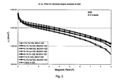
- FIG. 2 is a graph illustrating the magnetic J c values of Y 1-x M x Ba 2 Cu 3 O 7-z films compared to a reference Y123 film made using the same deposition conditions at 65K and H//c-axis.
- the present invention relates to a method of imparting magnetic flux pinning within a high temperature superconductor to improve current transport by introducing minute quantities of dopants into the material.
- substitution of small quantities (x ⁇ 0.02) of rare earth elements (La, Ce, Pr, Nd, Pm, Sm, Eu, Gd, Tb, Dy, Ho, Er, Tm, Yb, Lu) or other deleterious elements (Sc, etc.) for Y in Y123 thin films has been demonstrated to achieve the appropriate defect densities for enhanced flux pinning.
- “deleterious element” is intended to refer to a material that in large quantities would degrade the performance of the superconductor in an undesirable fashion.
- the method of the present invention enables enhanced flux pinning of the material while not significantly increasing the manufacturing cost of the HTS material. Additionally, the minute doping approach of the present invention can be used in all HTS deposition methods such as Metal-Organic Chemical Vapor Deposition (MOCVD), Metal-Organic Deposition (MOD), Pulsed Laser Deposition (PLD), sol-gel, sputtering and/or electrolytic deposition, etc., since it is not process dependent.
- MOCVD Metal-Organic Chemical Vapor Deposition
- MOD Metal-Organic Deposition
- PLD Pulsed Laser Deposition
- sol-gel sol-gel
- sputtering and/or electrolytic deposition sol-gel
- Coated conductor technology for biaxially aligned YBa 2 Cu 3 O 7-z , (Y123) on buffered metallic substrates with J c >1 MA/cm 2 offers great promise as a second generation, high temperature superconducting wire for use in generators and motors.
- Y123 has many useful properties at 77 K such as high critical current densities (J c ) and good flux pinning in applied magnetic fields, which is critical in most applications.
- J c when magnetic fields are applied parallel to the c-axis, J c will typically decrease by a factor of 10 to 100 within the range of 1 T ⁇ B appl ⁇ 5 T.
- J c H
- J c (H) places an upper limit on the magnetic field that can be produced/applied for a given coil design.
- REBa 2 Cu 3 O 7-z (RE123) (where RE stands for rare earth elements) superconductors have been considered for use in applications of thin film coated conductors because of their desirable high critical transition temperatures (T c ) ( ⁇ 92 K), and high critical current density (J c ) at 77 K in applied magnetic fields.
- T c critical transition temperatures
- J c critical current density
- Tb, Ce and Pr are divalent, having both +3 and +4 valance states and can act as pinning sites by localized lattice distortion or other potential mechanism. Even if a rare earth can readily form the proper REBCO superconducting phase, as in the case of Nd and La, they can be poor dopants in YBCO by substituting undesirably into the Ba site, degrading the superconductor's performance. However, in small quantities, these Ba substitutions can also act as a potential pinning mechanism. In addition, using small quantities of dopants allows the same processing conditions to be used for making high quality YBCO.
- Terbium does not degrade the T c of Y123 and the divalent nature of terbium (+3 and +4 valence states) can allow for Tb 4+ to act as pinning sites by alternate chemical bonding, localized lattice distortion, or other methods.
- the crystal ionic radii of Tb (+3) is 1.04 ⁇ which is quite close to the ionic radii of Y (+3) of 1.02 ⁇ .
- Tb123 is normally processed as a non-superconducting phase
- substitution of Tb123 for Y123 into a bulk or thin film superconductor has the potential to create localized regions of size on the order of one unit cell or larger of either reduced T c regions or potential site defects.
- Such regions can provide the non-superconducting pinning centers with particle densities approaching 1.5 ⁇ 3 ⁇ 10 11 cm ⁇ 2 which are necessary to pin magnetic fields of ⁇ 3 ⁇ 6 T.
- precursor materials i.e. laser ablation targets in the case of pulsed laser deposition
- Y 0.9 Tb 0.1 Ba 2 Cu 3 O 7-z powder was prepared from Y 2 O 3 , BaCO 3 , CuO, and Tb 4 O 7 powder (all nominally 99.99+% pure). The powders were dried, mixed, and then calcined at 850° C. and 880° C.
- This powder was then used to make two targets of compositions Y 0.9 Tb 0.1 Ba 2 Cu 3 O 7-z and Y 0.99 Tb 0.01 Ba 2 Cu 3 O 7-z with the second composition consisting of 10 mol % Y 0.9 Tb 0.1 Ba 2 Cu 3 O 7-z and 90 mol % Y123 powder.
- the targets were then fully reacted at 940° C. and 920° C. respectively for 50 hours.
- the Y 0.9 Tb 0.1 Ba 2 Cu 3 O 7-z target was found to be 84.8% dense and the Y 0.99 Tb 0.01 Ba 2 Cu 3 O 7-z target was found to be 88.7% dense.
- the estimated purity of the targets was 99.99+% pure.
- compositions of (Y,Tb) 123 films were deposited by pulsed laser deposition, using parameters and conditions optimized previously for Y123.
- the depositions were performed on strontium titanate (STO and lanthanum aluminate (LAO) substrates with the overall time for film growth being about 20 minutes.
- the laser pulse rate was 4 Hz and the laser fluence was ⁇ 3.2 J/cm 2 .
- the target-to-substrate distance was kept at 6 cm for all of the depositions.
- the oxygen pressure during the deposition was 300 mTorr for both of the Y,Tb-123 targets, as measured with capacitance manometer and convectron gauges within ⁇ 10% variation.
- Oxygen gas >99.997% purity
- the laser beam was scanned across the targets to improve thickness uniformity of the film.
- the LaAlO 3 (100) and SrTiO 3 (100) single crystal substrates were ultrasonically cleaned for 2 minutes, using first acetone followed by isopropyl alcohol.
- Crystalline substrates were provided by the manufacturer epitaxially polished on both sides of the LaAlO 3 and on one side for SrTiO 3 , and were attached to the heater using a thin layer of colloidal Ag paint.
- LAO and STO substrate sizes were ⁇ 3.2 ⁇ 3.2 mm 2 for magnetic Jc measurements.
- the background pressure in the chamber was reduced to ⁇ 1.4 ⁇ 10 ⁇ 4 torr prior to deposition.
- Samples were heated from room temperature to the deposition temperature of 775° C. at ⁇ 1270 ° C. /h. After deposition, the vacuum pumps and O 2 pressure control were shut off and the films were cooled radiantly from 775 ° C. to 500° C. while increasing the O 2 pressure to 1 atm. The temperature was then held at 500° C. for 30 minutes. The films were then cooled to room temperature.
- the (Y,Tb) 123 layer thickness was estimated by comparing previous deposition runs in the chamber using the same deposition parameters.
- Magnetic J c measurements were made with a Quantum Design Model 6000 Physical Property Measurement System (PPMS) with a vibrating sample magnetometer (VSM) attachment in fields of 0 to 9 T, and a ramp rate 0.01 T/s.
- Samples were subsequently acid-etched at the corners of the samples for thickness measurements.
- a P-15 Tencor profilometer was used to measure the thickness of the (Y,Tb) 123 films. Care was used to measure in twin-free areas of the LaAlO 3 substrates, which were observed visually at high magnification.
- the film thickness and dimensions of each sample were measured multiple times to reduce errors in determination of the superconducting volume and a to ⁇ 5%.
- FIGS. 1 and 2 show the results of J c measurements that were performed on several samples made using this invention.
- FIG. 1 shows the magnetic J c values of the Y 1-x M x Ba 2 Cu 3 O 7-z films at 77 K compared to a reference 123 film made using the same deposition conditions.
- FIG. 2 shows the magnetic J c values of the Y 1-x M x Ba 2 Cu 3 O 7-z films at 65 K compared to a reference 123 film made using the same deposition conditions.
- the minute doping method of the present invention has been demonstrated to provide enhanced flux pinning within HTS materials. Additionally, while the invention has been described in terms of pulsed laser deposition techniques, it is not considered so limited.
- the minute doping approach of the present invention can be used in all HTS deposition methods such as MOCVD, MOD, PLD, sol-gel, sputtering electrolytic deposition, etc., since it is not process dependent.
Landscapes
- Chemical & Material Sciences (AREA)
- Engineering & Computer Science (AREA)
- Manufacturing & Machinery (AREA)
- Chemical Kinetics & Catalysis (AREA)
- Materials Engineering (AREA)
- Mechanical Engineering (AREA)
- Metallurgy (AREA)
- Organic Chemistry (AREA)
- Physics & Mathematics (AREA)
- Optics & Photonics (AREA)
- Superconductors And Manufacturing Methods Therefor (AREA)
- Inorganic Compounds Of Heavy Metals (AREA)
Abstract
Description
Claims (12)
Priority Applications (2)
| Application Number | Priority Date | Filing Date | Title |
|---|---|---|---|
| US11/543,286 US7871663B1 (en) | 2005-10-03 | 2006-10-03 | Minute doping for YBCO flux pinning |
| US12/023,973 US8383552B1 (en) | 2006-10-03 | 2008-01-31 | Flux pinning of cuprate superconductors with nanoparticles |
Applications Claiming Priority (2)
| Application Number | Priority Date | Filing Date | Title |
|---|---|---|---|
| US72688205P | 2005-10-03 | 2005-10-03 | |
| US11/543,286 US7871663B1 (en) | 2005-10-03 | 2006-10-03 | Minute doping for YBCO flux pinning |
Related Child Applications (1)
| Application Number | Title | Priority Date | Filing Date |
|---|---|---|---|
| US12/023,973 Continuation-In-Part US8383552B1 (en) | 2006-10-03 | 2008-01-31 | Flux pinning of cuprate superconductors with nanoparticles |
Publications (1)
| Publication Number | Publication Date |
|---|---|
| US7871663B1 true US7871663B1 (en) | 2011-01-18 |
Family
ID=43479612
Family Applications (1)
| Application Number | Title | Priority Date | Filing Date |
|---|---|---|---|
| US11/543,286 Expired - Fee Related US7871663B1 (en) | 2005-10-03 | 2006-10-03 | Minute doping for YBCO flux pinning |
Country Status (1)
| Country | Link |
|---|---|
| US (1) | US7871663B1 (en) |
Cited By (4)
| Publication number | Priority date | Publication date | Assignee | Title |
|---|---|---|---|---|
| CN104364856A (en) * | 2012-06-08 | 2015-02-18 | 住友电气工业株式会社 | Starting-material solution for forming oxide superconductor |
| CN104380395A (en) * | 2012-05-31 | 2015-02-25 | 住友电气工业株式会社 | Oxide superconducting thin film and method for manufacturing same |
| CN108007895A (en) * | 2017-12-08 | 2018-05-08 | 北京鼎臣世纪超导科技有限公司 | A kind of method of checking R EBCO superconducting films precursor liquid quality |
| US10410781B2 (en) | 2015-03-24 | 2019-09-10 | Kabushiki Kaisha Toshiba | Superconductor and method for manufacturing same |
Citations (7)
| Publication number | Priority date | Publication date | Assignee | Title |
|---|---|---|---|---|
| US5998338A (en) | 1997-03-24 | 1999-12-07 | Superconductivity Research Laboratory | Method for preparing oxide superconductors |
| US6569360B2 (en) | 2000-09-11 | 2003-05-27 | Hengning Wu | Method of preparing metal matrix composite with textured compound |
| US6569811B1 (en) | 1997-06-11 | 2003-05-27 | University Of Cincinnati | Enhancement of JC in oxide superconductors |
| US6645313B2 (en) | 2002-02-22 | 2003-11-11 | Ut-Battelle, Llc | Powder-in-tube and thick-film methods of fabricating high temperature superconductors having enhanced biaxial texture |
| US6830776B1 (en) * | 2002-02-08 | 2004-12-14 | The United States Of America As Represented By The Secretary Of The Air Force | Method of manufacturing a high temperature superconductor |
| US20050043183A1 (en) * | 2000-10-23 | 2005-02-24 | Siu-Wai Chan | Thick film high temperature superconducting device supporting high critical currents and method for fabricating same |
| US20050159298A1 (en) * | 2004-01-16 | 2005-07-21 | American Superconductor Corporation | Oxide films with nanodot flux pinning centers |
-
2006
- 2006-10-03 US US11/543,286 patent/US7871663B1/en not_active Expired - Fee Related
Patent Citations (7)
| Publication number | Priority date | Publication date | Assignee | Title |
|---|---|---|---|---|
| US5998338A (en) | 1997-03-24 | 1999-12-07 | Superconductivity Research Laboratory | Method for preparing oxide superconductors |
| US6569811B1 (en) | 1997-06-11 | 2003-05-27 | University Of Cincinnati | Enhancement of JC in oxide superconductors |
| US6569360B2 (en) | 2000-09-11 | 2003-05-27 | Hengning Wu | Method of preparing metal matrix composite with textured compound |
| US20050043183A1 (en) * | 2000-10-23 | 2005-02-24 | Siu-Wai Chan | Thick film high temperature superconducting device supporting high critical currents and method for fabricating same |
| US6830776B1 (en) * | 2002-02-08 | 2004-12-14 | The United States Of America As Represented By The Secretary Of The Air Force | Method of manufacturing a high temperature superconductor |
| US6645313B2 (en) | 2002-02-22 | 2003-11-11 | Ut-Battelle, Llc | Powder-in-tube and thick-film methods of fabricating high temperature superconductors having enhanced biaxial texture |
| US20050159298A1 (en) * | 2004-01-16 | 2005-07-21 | American Superconductor Corporation | Oxide films with nanodot flux pinning centers |
Non-Patent Citations (9)
| Title |
|---|
| Fincher et al., Ce and Tb Substitution for Y in YBa2Cu3O7 Thin Films, Physical Review Letters, pp. 2902-2905, vol. 67, No. 20, Nov. 1991. |
| Fincher Jr. et al. "Ce and Tb substitution for Y in YBaCuO thin films", Physical Review Letters, vol. 67, No. 20, pp. 2902-2905, Nov. 11, 1991. * |
| Freibert et al., Anisotropic Magneto-resistivity in Pr and Tb Doped YBCO, American Physical Society Annual Meeting, abstract only, Mar. 1996. |
| Kell et al., "Tb and Ce Doped Y123 films processed by Pulsed Laser Ablation", conference, Oct. 2004. * |
| Kell et al., Tb and Ce Doped Y123 Films Processed by Pulsed Laser Deposition, Applied Superconductivity Conference Presentation, abstract only, Oct. 2004. |
| Paulius et al. "Enhancement of flux pinning by PR doping in YPrBaCuO", Physical Review B, vol. 47, No. 17 pp. 11627-11630. May 1, 1993. * |
| Staub et al., Tb Oxidation State and Hybridization in Y0.9Tb0.1Ba2Cu3O7−δ(δ=0.02, 0.84): A Magnetic-susceptibility and X-ray-absorption Study, Physical Review B, pp. 7085-7091, vol. 50, No. 10, Sep. 1994. |
| Staub et al., Tb Oxidation State and Hybridization in Y0.9Tb0.1Ba2Cu3O7-delta(delta=0.02, 0.84): A Magnetic-susceptibility and X-ray-absorption Study, Physical Review B, pp. 7085-7091, vol. 50, No. 10, Sep. 1994. |
| Tsurumi et al., High Tc Superconductivities of A2Ba4Cu6O14+y, Japanese Journal of Applied Physics, pp. 856-857, vol. 26, No. 5, May 1987. |
Cited By (5)
| Publication number | Priority date | Publication date | Assignee | Title |
|---|---|---|---|---|
| CN104380395A (en) * | 2012-05-31 | 2015-02-25 | 住友电气工业株式会社 | Oxide superconducting thin film and method for manufacturing same |
| CN104364856A (en) * | 2012-06-08 | 2015-02-18 | 住友电气工业株式会社 | Starting-material solution for forming oxide superconductor |
| US10410781B2 (en) | 2015-03-24 | 2019-09-10 | Kabushiki Kaisha Toshiba | Superconductor and method for manufacturing same |
| US11315713B2 (en) | 2015-03-24 | 2022-04-26 | Kabushiki Kaisha Toshiba | Superconductor and method for manufacturing same |
| CN108007895A (en) * | 2017-12-08 | 2018-05-08 | 北京鼎臣世纪超导科技有限公司 | A kind of method of checking R EBCO superconducting films precursor liquid quality |
Similar Documents
| Publication | Publication Date | Title |
|---|---|---|
| US6159610A (en) | Buffer layers on metal surfaces having biaxial texture as superconductor substrates | |
| JP2567460B2 (en) | Superconducting thin film and its manufacturing method | |
| US6764770B2 (en) | Buffer layers and articles for electronic devices | |
| US20130196856A1 (en) | Iron based superconducting structures and methods for making the same | |
| KR20020035837A (en) | Coated Conductor Thick Film Precursor | |
| US20110034336A1 (en) | CRITICAL CURRENT DENSITY ENHANCEMENT VIA INCORPORATION OF NANOSCALE Ba2(Y,RE)NbO6 IN REBCO FILMS | |
| US8623788B1 (en) | Flux pinning of cuprate superconductors with nanoparticles | |
| US5132282A (en) | High temperature superconductor-strontium titanate sapphire structures | |
| US20110034338A1 (en) | CRITICAL CURRENT DENSITY ENHANCEMENT VIA INCORPORATION OF NANOSCALE Ba2(Y,RE)TaO6 IN REBCO FILMS | |
| Ramesh et al. | Ferrimagnetic rare‐earth orthoferrites: A new, magnetic substrate for the growth of epitaxial Y‐Ba‐Cu‐O thin films | |
| US7737085B2 (en) | Coated conductors | |
| US7871663B1 (en) | Minute doping for YBCO flux pinning | |
| US5130294A (en) | High temperature superconductor-calcium titanate structures | |
| Kell et al. | Tb and Ce doped Y123 films processed by pulsed laser deposition | |
| KR970005158B1 (en) | Composite oxide superconducting thin film or wire and its manufacturing method | |
| US20110045984A1 (en) | Superconductive Compositions with Enhanced Flux Pinning | |
| RU2481673C1 (en) | Method to manufacture thin-film high-temperature superconductive material | |
| CN103069509A (en) | Base material for superconducting thin film, superconducting thin film, and method for manufacturing superconducting thin film | |
| Brorsson et al. | Laser‐deposited PrGaO3 films on SrTiO3 substrates and in YBa2Cu3O7/PrGaO3/YBa2Cu3O7 trilayers | |
| CN1041237A (en) | Film-forming method of bismuth-based composite oxide superconducting thin film | |
| Fartash et al. | Solid‐state reactions in high‐temperature superconductor‐ceramic interfaces; Y‐Ba‐Cu‐O on Al2O3 versus yttria‐stabilized ZrO2, and MgO | |
| US5141919A (en) | Superconducting device and method of producing superconducting thin film | |
| US20090036313A1 (en) | Coated superconducting materials | |
| JPH02175613A (en) | Production of oxide superconducting thin film | |
| Hosseini et al. | MOD growth of epitaxial cerium oxide buffer layer on LAO substrates for fabrication of c-axis oriented YBCO |
Legal Events
| Date | Code | Title | Description |
|---|---|---|---|
| AS | Assignment |
Owner name: KONINKLIJKE PHILIPS ELECTRONICS, N.V., NETHERLANDS Free format text: ASSIGNMENT OF ASSIGNORS INTEREST;ASSIGNORS:RITZ, ARND;VERGOHL, MICHAEL;HUNSCHE, BERNO;REEL/FRAME:018054/0547;SIGNING DATES FROM 20040129 TO 20040217 |
|
| AS | Assignment |
Owner name: AIR FORCE, UNITED STATES OF AMERICA AS REPRESENTED Free format text: GOVERNMENT INTEREST ASSIGNMENT;ASSIGNORS:BARNES, PAUL N.;KELL, JOSEPH W.;HAUGAN, TIMOTHY J.;SIGNING DATES FROM 20060123 TO 20061012;REEL/FRAME:018814/0605 |
|
| FPAY | Fee payment |
Year of fee payment: 4 |
|
| FEPP | Fee payment procedure |
Free format text: MAINTENANCE FEE REMINDER MAILED (ORIGINAL EVENT CODE: REM.); ENTITY STATUS OF PATENT OWNER: LARGE ENTITY |
|
| LAPS | Lapse for failure to pay maintenance fees |
Free format text: PATENT EXPIRED FOR FAILURE TO PAY MAINTENANCE FEES (ORIGINAL EVENT CODE: EXP.); ENTITY STATUS OF PATENT OWNER: LARGE ENTITY |
|
| STCH | Information on status: patent discontinuation |
Free format text: PATENT EXPIRED DUE TO NONPAYMENT OF MAINTENANCE FEES UNDER 37 CFR 1.362 |
|
| FP | Lapsed due to failure to pay maintenance fee |
Effective date: 20190118 |