US7835176B2 - Implementing enhanced dual mode SRAM performance screen ring oscillator - Google Patents
Implementing enhanced dual mode SRAM performance screen ring oscillator Download PDFInfo
- Publication number
- US7835176B2 US7835176B2 US12/360,230 US36023009A US7835176B2 US 7835176 B2 US7835176 B2 US 7835176B2 US 36023009 A US36023009 A US 36023009A US 7835176 B2 US7835176 B2 US 7835176B2
- Authority
- US
- United States
- Prior art keywords
- sram
- input
- base blocks
- wordline
- sram cell
- Prior art date
- Legal status (The legal status is an assumption and is not a legal conclusion. Google has not performed a legal analysis and makes no representation as to the accuracy of the status listed.)
- Expired - Fee Related, expires
Links
Images


Classifications
-
- G—PHYSICS
- G11—INFORMATION STORAGE
- G11C—STATIC STORES
- G11C11/00—Digital stores characterised by the use of particular electric or magnetic storage elements; Storage elements therefor
- G11C11/21—Digital stores characterised by the use of particular electric or magnetic storage elements; Storage elements therefor using electric elements
- G11C11/34—Digital stores characterised by the use of particular electric or magnetic storage elements; Storage elements therefor using electric elements using semiconductor devices
- G11C11/40—Digital stores characterised by the use of particular electric or magnetic storage elements; Storage elements therefor using electric elements using semiconductor devices using transistors
- G11C11/41—Digital stores characterised by the use of particular electric or magnetic storage elements; Storage elements therefor using electric elements using semiconductor devices using transistors forming static cells with positive feedback, i.e. cells not needing refreshing or charge regeneration, e.g. bistable multivibrator or Schmitt trigger
- G11C11/413—Auxiliary circuits, e.g. for addressing, decoding, driving, writing, sensing, timing or power reduction
- G11C11/417—Auxiliary circuits, e.g. for addressing, decoding, driving, writing, sensing, timing or power reduction for memory cells of the field-effect type
-
- G—PHYSICS
- G11—INFORMATION STORAGE
- G11C—STATIC STORES
- G11C11/00—Digital stores characterised by the use of particular electric or magnetic storage elements; Storage elements therefor
- G11C11/21—Digital stores characterised by the use of particular electric or magnetic storage elements; Storage elements therefor using electric elements
- G11C11/34—Digital stores characterised by the use of particular electric or magnetic storage elements; Storage elements therefor using electric elements using semiconductor devices
- G11C11/40—Digital stores characterised by the use of particular electric or magnetic storage elements; Storage elements therefor using electric elements using semiconductor devices using transistors
- G11C11/41—Digital stores characterised by the use of particular electric or magnetic storage elements; Storage elements therefor using electric elements using semiconductor devices using transistors forming static cells with positive feedback, i.e. cells not needing refreshing or charge regeneration, e.g. bistable multivibrator or Schmitt trigger
- G11C11/412—Digital stores characterised by the use of particular electric or magnetic storage elements; Storage elements therefor using electric elements using semiconductor devices using transistors forming static cells with positive feedback, i.e. cells not needing refreshing or charge regeneration, e.g. bistable multivibrator or Schmitt trigger using field-effect transistors only
-
- G—PHYSICS
- G11—INFORMATION STORAGE
- G11C—STATIC STORES
- G11C11/00—Digital stores characterised by the use of particular electric or magnetic storage elements; Storage elements therefor
- G11C11/21—Digital stores characterised by the use of particular electric or magnetic storage elements; Storage elements therefor using electric elements
- G11C11/34—Digital stores characterised by the use of particular electric or magnetic storage elements; Storage elements therefor using electric elements using semiconductor devices
- G11C11/40—Digital stores characterised by the use of particular electric or magnetic storage elements; Storage elements therefor using electric elements using semiconductor devices using transistors
- G11C11/41—Digital stores characterised by the use of particular electric or magnetic storage elements; Storage elements therefor using electric elements using semiconductor devices using transistors forming static cells with positive feedback, i.e. cells not needing refreshing or charge regeneration, e.g. bistable multivibrator or Schmitt trigger
- G11C11/413—Auxiliary circuits, e.g. for addressing, decoding, driving, writing, sensing, timing or power reduction
-
- G—PHYSICS
- G11—INFORMATION STORAGE
- G11C—STATIC STORES
- G11C8/00—Arrangements for selecting an address in a digital store
- G11C8/18—Address timing or clocking circuits; Address control signal generation or management, e.g. for row address strobe [RAS] or column address strobe [CAS] signals
-
- G—PHYSICS
- G11—INFORMATION STORAGE
- G11C—STATIC STORES
- G11C7/00—Arrangements for writing information into, or reading information out from, a digital store
- G11C7/10—Input/output [I/O] data interface arrangements, e.g. I/O data control circuits, I/O data buffers
- G11C7/1015—Read-write modes for single port memories, i.e. having either a random port or a serial port
- G11C7/1045—Read-write mode select circuits
Definitions
- the present invention relates generally to the data processing field, and more particularly, relates to a method and circuit for implementing an enhanced dual-mode eight-transistor (8T) static random access memory (SRAM) performance screen ring oscillator (PSRO), and a design structure on which the subject circuit resides.
- 8T enhanced dual-mode eight-transistor
- SRAM static random access memory
- PSRO performance screen ring oscillator
- Prior art circuits exists to determine 6T SRAM read performance and 8T SRAM write-through performance.
- frequency is a function of only read performance and not write performance.
- frequency is only a function of write-through performance.
- PSRO enhanced SRAM read performance sort ring oscillator
- a pair of parallel reverse polarity connected inverters defines a static latch or cross-coupled memory cell.
- the SRAM cell includes independent left and right wordlines providing a respective gate input to a pair of access transistors used to access to the memory cell.
- the SRAM cell includes a voltage supply connection to one side of the static latch. For example, a complement side of the static latch is connected to the voltage supply.
- a plurality of the SRAM cells is assembled together to form a SRAM base block.
- a plurality of the SRAM base blocks is connected together to form the SRAM read PSRO.
- FIG. 1 illustrates a conventional eight-transistor (8T) static random access memory (SRAM) cell.
- the prior art 8T SRAM cell includes four transistors defining a pair of parallel reverse polarity connected inverters 102 , 104 for storing data, a pair of N-channel field effect transistors (NFETs) 106 , 108 respectively connected to a respective side of the static latch and a respective one of a write bit line pair WBLC, WBLT, and receiving a gate input WRITE WORDLINE that is activated to turn on NFETs 106 , 108 to perform a write operation, and a pair of series connected NFETs 110 , 112 connected to a read bitline RBLT with NFET 110 receiving a gate input READ_WORDLINE, and NFET 112 receiving a gate input connected to a first side or complement side (CMP) of the static latch, as shown in FIG. 1 .
- NFET 110 is activated by the gate input READ_WORDLINE
- An invention is needed to separately monitor read and write-through performance of an 8T SRAM cell using an unmodified SRAM cell.
- Principal aspects of the present invention are to provide a method and circuit for implementing an enhanced dual-mode eight-transistor (8T) static random access memory (SRAM) performance screen ring oscillator (PSRO), and a design structure on which the subject circuit resides.
- Other important aspects of the present invention are to provide such method, circuit and design structure substantially without negative effect and that overcome many of the disadvantages of prior art arrangements.
- the dual-mode SRAM PSRO includes a plurality of SRAM base blocks connected together in a chain. Each of the plurality of SRAM base blocks includes an eight-transistor (8T) SRAM cell, a local evaluation circuit and a logic function coupled to the SRAM cell and the local evaluation circuit.
- the eight-transistor (8T) static random access memory (SRAM) cell is an unmodified 8T SRAM cell.
- the dual-mode SRAM PSRO includes a write-through mode of operation, where the output frequency is determined by write-through performance of the 8T SRAM cell; and a read mode of operation, where the output frequency is determined by read performance of the 8T SRAM cell.
- the dual-mode SRAM PSRO separately monitors read performance and write-through performance of the 8T SRAM cell.
- the dual-mode SRAM PSRO directly tracks the performance of 8T SRAM macros much closer than standard logic PSROs.
- the dual-mode SRAM PSRO independently measures read performance and write-through performance, mirroring functional mode SRAM operation.
- FIG. 1 illustrates a conventional eight-transistor (8T) static random access memory (SRAM) cell
- FIG. 2 illustrates an exemplary SRAM base block using an unmodified SRAM cell for implementing a dual-mode static random access memory (SRAM) performance screen ring oscillator (PSRO) in accordance with the preferred embodiment;
- SRAM static random access memory
- PSRO screen ring oscillator
- FIG. 3 illustrates an exemplary SRAM performance screen ring oscillator (PSRO) including a plurality of SRAM base blocks of FIG. 2 in accordance with the preferred embodiment;
- PSRO SRAM performance screen ring oscillator
- FIGS. 4 , 5 , 6 A, 6 B, and 7 are charts illustrating operation of the exemplary dual-mode SRAM performance screen ring oscillator (PSRO) of FIG. 3 in accordance with the preferred embodiment.
- PSRO screen ring oscillator
- FIG. 8 is a flow diagram of a design process used in semiconductor design, manufacturing, and/or test.
- an unmodified eight-transistor (8T) static random access memory (SRAM) cell is used to create an 8T SRAM performance screen ring oscillator (PSRO) that effectively and efficiently separately monitors both read and write performance of 8T SRAM macros.
- 8T SRAM PSRO of the invention provides accurate representations of functional SRAM performance and has a robust circuit implementation.
- the 8T SRAM PSRO includes one mode where the output frequency is determined by write-through performance of the cell, and in the other mode the output frequency is determined by read performance of the cell.
- the 8T SRAM PSRO of the invention provides a significant improvement over the prior art, which suffers from design problems and poor performance matching. Also none of the prior art arrangements can measure both read performance and write performance in the same circuit.
- FIG. 2 there is shown exemplary SRAM base block using an unmodified SRAM cell generally designated by the reference character 200 in accordance with the preferred embodiment.
- SRAM base block 200 is used for implementing a dual-mode static random access memory (SRAM) performance screen ring oscillator (PSRO), as illustrated in FIG. 3 .
- SRAM static random access memory
- PSRO screen ring oscillator
- SRAM base block 200 includes an unmodified eight-transistor (8T) static random access memory (SRAM) cell 201 .
- the 8T SRAM cell 201 includes four transistors defining a pair of parallel reverse polarity connected inverters 202 , 204 for storing data, a pair of N-channel field effect transistors (NFETs) 206 , 208 respectively connected to a respective side of the static latch and a respective one of a write bit line pair WBLC, WBLT, and receiving a write wordline gate input WWL that is activated to turn on NFETs 206 , 208 to perform a write operation, and a pair of series connected NFETs 210 , 212 connected to a read bitline RBLT with NFET 210 receiving a read wordline gate input RWL, and NFET 212 receiving a gate input connected to a first side or complement side (CMP) of the static latch NFET 210 is activated by the read wordline gate input RWL to perform a read operation
- SRAM base block 200 includes a logic function generally designated by the reference character 214 for applying the read wordline gate input RWL, the write wordline gate input WWL, and the write bit line pair WBLC, WBLT to the SRAM cell 201 .
- the logic function 214 includes a NAND gate 216 receiving a wordline input WLIN and a reset signal RESET_B. An output of NAND gate 216 at NET 1 is applied to a first input of a NAND gate 218 and to an inverter 220 .
- the logic function 214 includes a NOR gate 222 receiving the wordline input WLIN and a read input R_WB.
- the NORed output provides the write bit line WBLT to NFET 206 .
- the NORed output is applied to an inverter 224 , which provides the write bit line WBLC to NFET 208 .
- the read input R_WB is applied to an inverter 226 , which provides an inverted read input R_WB_B applied to a 3-input NAND gate 228 .
- the reset signal RESET_B and the output of NAND gate 216 at NET 1 are applied to other inputs the 3-input NAND gate 228 .
- An output of the 3-input NAND gate 228 provides a write wordline input WWL applied to a gate input of both NFETs 206 , 208 .
- SRAM base block 200 includes a local evaluation circuit 230 .
- the local evaluation circuit 230 includes a P-channel field effect transistor (PFET) 232 connected between a voltage supply rail VCC and a connection of the read bitline RBLT output of SRAM cell 201 and a first input of a NAND gate 234 .
- the output PCH of inverter 220 applies a gate input to the PFET 234 .
- a second input of the NAND gate 234 is connected the voltage supply rail VCC.
- the NAND gate 234 provides the output WLOUT of the SRAM BASE BLOCK 200 .
- SRAM base block 200 is shown with a single modified SRAM cell 221 , it should be understood that multiple dummy SRAM cells can be connected to the same write bit line pair WBLT, WBLC and read bitline RBLT.
- Dummy SRAM cells 201 optionally are added in parallel with the SRAM cell 201 shown in FIG. 2 , to match the bitline capacitance of the dual-mode 8T SRAM PSRO 300 as illustrated in FIG. 3 , to the bitline capacitance of functional SRAM circuits.
- FIG. 3 there is shown an 8T SRAM dual-mode performance screen ring oscillator (PSRO) generally designated by the reference character 300 in accordance with the preferred embodiment.
- PSRO screen ring oscillator
- the 8T SRAM PSRO 300 includes a chain 302 of a plurality of SRAM base blocks 200 , # 1 -N connected together in a chain as illustrated.
- the reset signal RESET_B is brought into all SRAM base blocks 200 , # 1 -N in parallel.
- the read input signal R_WB is brought into all SRAM base blocks 200 , # 1 -N in parallel.
- the output WLOUT of SRAM base blocks 200 # 1 -(N ⁇ 1) is connected to the input WLIN in the next SRAM base block 200 # 2 -N.
- the output WLOUT of SRAM base block 200 #N is coupled to the input WLIN in the SRAM base block 200 # 1 through the illustrated logic gates.
- the 8T SRAM PSRO 300 provides a ring oscillator output signal RINGOUT.
- the wordline input WLIN is applied to the first SRAM base block 200 , # 1 and the output WLOUT of the SRAM base block 200 , #N provides a feedback signal applied to an inverter 304 providing an inverted feedback signal applied to a NAND gate 306 .
- the inverted feedback signal is combined with a control signal GO by NAND gate 306 .
- the NAND gate 306 is used to stop and start the ring operation.
- the GO signal of the feedback two input NAND gate 306 stops the ring operation when low and allows the ring to run when high.
- NAND gate 306 The output of NAND gate 306 is applied to an inverter 308 providing an inverted controlled feedback signal applied to a NAND gate 310 and coupled to the input WLIN in the SRAM base block 200 # 1 . Since the operation is a series write and read but parallel reset the output RINGOUT of the 8T SRAM PSRO 300 is a short pulse.
- a plurality of inverters 312 , 314 , 316 , 318 optionally is included in a ring output path to a second input to NAND gate 310 to expand the pulse width of the ring oscillator output signal RINGOUT for sending across an associated chip.
- a final pair of inverters 320 , 322 optionally is connected to the output of NAND gate 310 , which provide the ring oscillator output signal RINGOUT.
- the reset signal RESET_B is applied in parallel to each of the plurality of the SRAM base blocks 200 so that the period of the ring oscillator output signal RINGOUT is a function of many series write and read operations but only a single reset time.
- 8T SRAM base block 200 illustrated in FIG. 2 and used in 8T SRAM PSRO 300 may be understood as follows:
- the RESET_B signal will start high with WLIN low, applied to the gate of NAND gate 216 .
- Input R_WB is a DC signal, and in read performance mode it is always high. In read performance mode, WBLT, WBLC, and WWL are also DC signals.
- the reset signal RESET_B is NORed with R_WB to make WBLT node of the SRAM cell 201 to go low and WBLC node of the SRAM cell 201 to go high.
- R_WB_B being low applied to NAND gate 227 makes WWL always high. This configuration forces node TRU of the SRAM cell 201 to be low and node CMP of the SRAM cell 201 to be high in read performance mode.
- FIG. 3 shows the entire circuit 8T SRAM PSRO 300 where many base blocks 200 , # 1 -N are connected together, where WLOUT is connected to WLIN of the next base block and this operation now repeats.
- the RESET_B signal is significant after this reading of the 8T SRAM cell has propagated through all of the base blocks 200 .
- the feedback is inverted to reset all the 8T SRAM cells in parallel.
- RESET_B goes low causing NET 1 to go high and RWL and PCH to go low.
- the waveforms are shown in FIGS. 4 , 5 , 6 A, 6 B, and 7 .
- the RESET_B signal will start high with WLIN low, applied to the gate of NAND gate 216 .
- Input R_WB applied to NOR gate 222 and NAND gate 218 is a DC signal, and in write-through performance mode Input R_WB is always low, which the output R_WB_B of inverter 226 always high.
- output RWL of NAND gate 218 is also a DC signal and output RWL is always high.
- the reset signal RESET_B is NORed with R_WB to make WBLT node of the SRAM cell 201 low and WBLC node of the SRAM cell 201 high.
- Input WLIN is low so output NET 1 of NAND gate 216 is high. All “1's” at the input of NAND gate 228 make gate input WWL of NFETs 206 , 208 low.
- the signal RESET_B is significant after this write-through of the 8T SRAM cell 201 has propagated through all of the base blocks 200 , # 1 -N.
- the feedback is inverted to reset all the 8T SRAM cells in parallel.
- the signal RESET_B goes low causing SRAM cell node WBLT to go high, SRAM cell node WBLC to go low, and SRAM cell node WWL to go high. This writes the opposite state back to the SRAM cell 201 .
- output NET 1 of NAND gate 216 goes high causing node PCH to go low and PFET 232 pulls read bitline RBLT high and NAND gate 234 in the local evaluation circuit 230 causes WLOUT to go low.
- the waveforms are shown in FIGS. 4 , 5 , 6 A, 6 B, and 7 .
- FIGS. 4 , 5 , 6 A. 6 B, and 7 there are shown waveforms illustrating the operation of the dual mode SRAM performance screen ring oscillator (PSRO) 300 in accordance with the preferred embodiment.
- PSRO dual mode SRAM performance screen ring oscillator
- FIG. 4 shows the simulated top level waveforms of the dual mode SRAM PSRO 300 .
- the ring oscillator output signal RINGOUT produces a series of repeated pulses where the period is determined by the series write-through operations or read operations and single reset operation per pulse. Note that the period of the RINGOUT pulse is larger for the write-through operations than the read operations.
- FIG. 5 shows the simulated waveforms of the top level nets between the base SRAM building blocks 200 of the dual mode SRAM PSRO 300 .
- Eight base SRAM blocks 200 were used in the embodiment of the circuit simulated to generate the waveforms of FIG. 5 .
- FIG. 5 illustrates exemplary illustrated waveforms WLOUT coupled between the base building blocks 200 and labeled STG 1 -STG 8 with an input waveform WLIN applied to the first block 200 , # 1 .
- FIG. 5 shows how the reset is done in parallel with each RINGOUT pulse and labeled Parallel Restore and the following series nature of the write-through operations and read operations labeled Series Write-through and Series Read.
- FIG. 6A shows the simulated waveforms of the internal read bitlines (RBLT) inside the base SRAM building blocks 200 of the dual mode SRAM PSRO 300 for the write through performance mode.
- FIG. 6A illustrates the parallel reset of the entire dual mode SRAM PSRO 300 labeled Parallel Restore and the series nature of the write-through operations labeled Series Write-through.
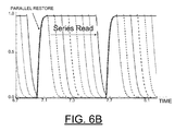
- FIG. 6B shows the simulated waveforms of the internal read bitlines (RBLT) inside the base SRAM building blocks 200 of the dual mode SRAM PSRO 300 for the read performance mode.
- FIG. 6B illustrates the parallel reset of the entire dual mode SRAM PSRO 300 labeled Parallel Restore and the series nature of the read operations labeled Series Read.
- FIG. 7 shows the simulated waveforms of the internal true node TRU of the 8T SRAM cells 201 inside the base SRAM building blocks 200 of the dual mode SRAM PSRO 300 .
- FIG. 7 illustrates the parallel reset of the entire dual mode SRAM PSRO 300 labeled PARALLEL RESTORE and the series nature of the write-through and read operations labeled SERIES WRITE-THRU. In the read performance mode, node TRU stays low.
- FIG. 8 shows a block diagram of an example design flow 800 .
- Design flow 800 may vary depending on the type of IC being designed.
- a design flow 800 for building an application specific IC (ASIC) may differ from a design flow 800 for designing a standard component.
- Design structure 802 is preferably an input to a design process 804 and may come from an IP provider, a core developer, or other design company or may be generated by the operator of the design flow, or from other sources.
- Design structure 802 comprises circuits 100 , 200 , 300 in the form of schematics or HDL, a hardware-description language, for example, Verilog, VHDL, C, and the like.
- Design structure 802 may be contained on one or more machine readable medium.
- design structure 802 may be a text file or a graphical representation of circuits 100 , 200 , 300 .
- Design process 804 preferably synthesizes, or translates, circuits 100 , 200 , 300 into a netlist 806 , where netlist 806 is, for example, a list of wires, transistors, logic gates, control circuits, I/O, models, etc. that describes the connections to other elements and circuits in an integrated circuit design and recorded on at least one of machine readable medium. This may be an iterative process in which netlist 806 is resynthesized one or more times depending on design specifications and parameters for the circuits.
- Design process 804 may include using a variety of inputs; for example, inputs from library elements 808 which may house a set of commonly used elements, circuits, and devices, including models, layouts, and symbolic representations, for a given manufacturing technology, such as different technology nodes, 32 nm, 45 nm, 90 nm, and the like, design specifications 810 , characterization data 812 , verification data 814 , design rules 816 , and test data files 818 , which may include test patterns and other testing information. Design process 804 may further include, for example, standard circuit design processes such as timing analysis, verification, design rule checking, place and route operations, and the like.
- standard circuit design processes such as timing analysis, verification, design rule checking, place and route operations, and the like.
- Design process 804 preferably translates an embodiment of the invention as shown in FIGS. 1 , 2 , and 3 along with any additional integrated circuit design or data (if applicable), into a second design structure 820 .
- Design structure 820 resides on a storage medium in a data format used for the exchange of layout data of integrated circuits, for example, information stored in a GDSII (GDS2), GL1, OASIS, or any other suitable format for storing such design structures.
- Design structure 820 may comprise information such as, for example, test data files, design content files, manufacturing data, layout parameters, wires, levels of metal, vias, shapes, data for routing through the manufacturing line, and any other data required by a semiconductor manufacturer to produce an embodiment of the invention as shown in FIGS.
- Design structure 820 may then proceed to a stage 822 where, for example, design structure 820 proceeds to tape-out, is released to manufacturing, is released to a mask house, is sent to another design house, is sent back to the customer, and the like.
Landscapes
- Engineering & Computer Science (AREA)
- Microelectronics & Electronic Packaging (AREA)
- Computer Hardware Design (AREA)
- For Increasing The Reliability Of Semiconductor Memories (AREA)
- Static Random-Access Memory (AREA)
Abstract
Description
Claims (20)
Priority Applications (1)
| Application Number | Priority Date | Filing Date | Title |
|---|---|---|---|
| US12/360,230 US7835176B2 (en) | 2009-01-27 | 2009-01-27 | Implementing enhanced dual mode SRAM performance screen ring oscillator |
Applications Claiming Priority (1)
| Application Number | Priority Date | Filing Date | Title |
|---|---|---|---|
| US12/360,230 US7835176B2 (en) | 2009-01-27 | 2009-01-27 | Implementing enhanced dual mode SRAM performance screen ring oscillator |
Publications (2)
| Publication Number | Publication Date |
|---|---|
| US20100188888A1 US20100188888A1 (en) | 2010-07-29 |
| US7835176B2 true US7835176B2 (en) | 2010-11-16 |
Family
ID=42354031
Family Applications (1)
| Application Number | Title | Priority Date | Filing Date |
|---|---|---|---|
| US12/360,230 Expired - Fee Related US7835176B2 (en) | 2009-01-27 | 2009-01-27 | Implementing enhanced dual mode SRAM performance screen ring oscillator |
Country Status (1)
| Country | Link |
|---|---|
| US (1) | US7835176B2 (en) |
Cited By (4)
| Publication number | Priority date | Publication date | Assignee | Title |
|---|---|---|---|---|
| US8754696B2 (en) | 2012-07-26 | 2014-06-17 | International Business Machines Corporation | Ring oscillator |
| US9097765B1 (en) | 2014-05-08 | 2015-08-04 | International Business Machines Corporation | Performance screen ring oscillator formed from multi-dimensional pairings of scan chains |
| US9128151B1 (en) | 2014-05-08 | 2015-09-08 | International Business Machines Corporation | Performance screen ring oscillator formed from paired scan chains |
| US9188643B2 (en) | 2012-11-13 | 2015-11-17 | Globalfoundries Inc. | Flexible performance screen ring oscillator within a scan chain |
Families Citing this family (3)
| Publication number | Priority date | Publication date | Assignee | Title |
|---|---|---|---|---|
| TWI483251B (en) * | 2012-02-24 | 2015-05-01 | Univ Nat Chiao Tung | An oscillator based on a 6t sram for measuring the bias temperature instability |
| US11069424B2 (en) * | 2018-11-07 | 2021-07-20 | Arm Limited | Sensor for performance variation of memory read and write characteristics |
| US11443819B2 (en) | 2020-07-24 | 2022-09-13 | Taiwan Semiconductor Manufacturing Company, Ltd. | Memory device, integrated circuit device and method |
Citations (3)
| Publication number | Priority date | Publication date | Assignee | Title |
|---|---|---|---|---|
| US6370073B2 (en) * | 1998-10-01 | 2002-04-09 | Monlithic System Technology, Inc. | Single-port multi-bank memory system having read and write buffers and method of operating same |
| US7082067B2 (en) | 2004-09-03 | 2006-07-25 | Lsi Logic Corporation | Circuit for verifying the write speed of SRAM cells |
| US7142064B2 (en) | 2004-10-26 | 2006-11-28 | International Business Machines Corporation | SRAM ring oscillator |
Family Cites Families (1)
| Publication number | Priority date | Publication date | Assignee | Title |
|---|---|---|---|---|
| US9251212B2 (en) * | 2009-03-27 | 2016-02-02 | Business Objects Software Ltd. | Profiling in a massive parallel processing environment |
-
2009
- 2009-01-27 US US12/360,230 patent/US7835176B2/en not_active Expired - Fee Related
Patent Citations (3)
| Publication number | Priority date | Publication date | Assignee | Title |
|---|---|---|---|---|
| US6370073B2 (en) * | 1998-10-01 | 2002-04-09 | Monlithic System Technology, Inc. | Single-port multi-bank memory system having read and write buffers and method of operating same |
| US7082067B2 (en) | 2004-09-03 | 2006-07-25 | Lsi Logic Corporation | Circuit for verifying the write speed of SRAM cells |
| US7142064B2 (en) | 2004-10-26 | 2006-11-28 | International Business Machines Corporation | SRAM ring oscillator |
Non-Patent Citations (1)
| Title |
|---|
| U.S. Appl. No. 11/782,808, filed Jul. 25, 2007, by Chad Allen Adams, Todd Alan Christensen, Travis Reynold Hebig, and Kirk David Peterson, entitled "Method and Apparatus for Implementing Enhanced SRAM Read Performance Sort Ring Oscillator (PSRO)". |
Cited By (4)
| Publication number | Priority date | Publication date | Assignee | Title |
|---|---|---|---|---|
| US8754696B2 (en) | 2012-07-26 | 2014-06-17 | International Business Machines Corporation | Ring oscillator |
| US9188643B2 (en) | 2012-11-13 | 2015-11-17 | Globalfoundries Inc. | Flexible performance screen ring oscillator within a scan chain |
| US9097765B1 (en) | 2014-05-08 | 2015-08-04 | International Business Machines Corporation | Performance screen ring oscillator formed from multi-dimensional pairings of scan chains |
| US9128151B1 (en) | 2014-05-08 | 2015-09-08 | International Business Machines Corporation | Performance screen ring oscillator formed from paired scan chains |
Also Published As
| Publication number | Publication date |
|---|---|
| US20100188888A1 (en) | 2010-07-29 |
Similar Documents
| Publication | Publication Date | Title |
|---|---|---|
| US7724565B2 (en) | Apparatus and method for small signal sensing in an SRAM cell utilizing PFET access devices | |
| US7835176B2 (en) | Implementing enhanced dual mode SRAM performance screen ring oscillator | |
| US7684263B2 (en) | Method and circuit for implementing enhanced SRAM write and read performance ring oscillator | |
| US7788554B2 (en) | Design structure embodied in a machine readable medium for implementing SRAM cell write performance evaluation | |
| US7609542B2 (en) | Implementing enhanced SRAM read performance sort ring oscillator (PSRO) | |
| JP4005535B2 (en) | Semiconductor memory device | |
| US7890907B2 (en) | Computer program product for designing memory circuits having single-ended memory cells with improved read stability | |
| US6901003B2 (en) | Lower power and reduced device split local and continuous bitline for domino read SRAMs | |
| US7082067B2 (en) | Circuit for verifying the write speed of SRAM cells | |
| US8213249B2 (en) | Implementing low power data predicting local evaluation for double pumped arrays | |
| US7724586B2 (en) | Implementing local evaluation of domino read SRAM with enhanced SRAM cell stability with minimized area usage | |
| US9947419B1 (en) | Apparatus and method for implementing design for testability (DFT) for bitline drivers of memory circuits | |
| Arslan et al. | Variation-tolerant SRAM sense-amplifier timing using configurable replica bitlines | |
| US7724585B2 (en) | Implementing local evaluation of domino read SRAM with enhanced SRAM cell stability | |
| US8824196B2 (en) | Single cycle data copy for two-port SRAM | |
| Nalam et al. | Dynamic write limited minimum operating voltage for nanoscale SRAMs | |
| US8659937B2 (en) | Implementing low power write disabled local evaluation for SRAM | |
| US8522178B2 (en) | Re-modeling a memory array for accurate timing analysis | |
| US8675427B2 (en) | Implementing RC and coupling delay correction for SRAM | |
| US7925950B2 (en) | Implementing enhanced array access time tracking with logic built in self test of dynamic memory and random logic | |
| Medeiros et al. | Evaluating the impact of temperature on dynamic fault behaviour of FinFET-based SRAMs with resistive defects | |
| US11967365B2 (en) | Bitcell architecture with time-multiplexed ports | |
| US6654937B1 (en) | Register file timing using static timing tools | |
| Ciampolini | SRAM Bitcell Functionality Under Body-Bias | |
| JPH08263999A (en) | Fault detection method in sram and cell of sram |
Legal Events
| Date | Code | Title | Description |
|---|---|---|---|
| AS | Assignment |
Owner name: INTERNATIONAL BUSINESS MACHINES CORPORATION, NEW Y Free format text: ASSIGNMENT OF ASSIGNORS INTEREST;ASSIGNORS:ADAMS, CHAD ALLEN;CHRISTENSEN, TODD ALAN;FREIBURGER, PETER THOMAS;AND OTHERS;REEL/FRAME:022159/0973 Effective date: 20090122 |
|
| REMI | Maintenance fee reminder mailed | ||
| FPAY | Fee payment |
Year of fee payment: 4 |
|
| SULP | Surcharge for late payment | ||
| AS | Assignment |
Owner name: GLOBALFOUNDRIES U.S. 2 LLC, NEW YORK Free format text: ASSIGNMENT OF ASSIGNORS INTEREST;ASSIGNOR:INTERNATIONAL BUSINESS MACHINES CORPORATION;REEL/FRAME:036550/0001 Effective date: 20150629 |
|
| AS | Assignment |
Owner name: GLOBALFOUNDRIES INC., CAYMAN ISLANDS Free format text: ASSIGNMENT OF ASSIGNORS INTEREST;ASSIGNORS:GLOBALFOUNDRIES U.S. 2 LLC;GLOBALFOUNDRIES U.S. INC.;REEL/FRAME:036779/0001 Effective date: 20150910 |
|
| FEPP | Fee payment procedure |
Free format text: MAINTENANCE FEE REMINDER MAILED (ORIGINAL EVENT CODE: REM.) |
|
| AS | Assignment |
Owner name: WILMINGTON TRUST, NATIONAL ASSOCIATION, DELAWARE Free format text: SECURITY AGREEMENT;ASSIGNOR:GLOBALFOUNDRIES INC.;REEL/FRAME:049490/0001 Effective date: 20181127 |
|
| LAPS | Lapse for failure to pay maintenance fees |
Free format text: PATENT EXPIRED FOR FAILURE TO PAY MAINTENANCE FEES (ORIGINAL EVENT CODE: EXP.); ENTITY STATUS OF PATENT OWNER: LARGE ENTITY |
|
| STCH | Information on status: patent discontinuation |
Free format text: PATENT EXPIRED DUE TO NONPAYMENT OF MAINTENANCE FEES UNDER 37 CFR 1.362 |
|
| FP | Lapsed due to failure to pay maintenance fee |
Effective date: 20181116 |
|
| AS | Assignment |
Owner name: GLOBALFOUNDRIES INC., CAYMAN ISLANDS Free format text: RELEASE BY SECURED PARTY;ASSIGNOR:WILMINGTON TRUST, NATIONAL ASSOCIATION;REEL/FRAME:054636/0001 Effective date: 20201117 |
|
| AS | Assignment |
Owner name: GLOBALFOUNDRIES U.S. INC., NEW YORK Free format text: RELEASE BY SECURED PARTY;ASSIGNOR:WILMINGTON TRUST, NATIONAL ASSOCIATION;REEL/FRAME:056987/0001 Effective date: 20201117 |