US7830991B2 - Frequency selective automatic gain control with dual non-symmetric attack and release times and interference detection feature - Google Patents
Frequency selective automatic gain control with dual non-symmetric attack and release times and interference detection feature Download PDFInfo
- Publication number
- US7830991B2 US7830991B2 US11/243,289 US24328905A US7830991B2 US 7830991 B2 US7830991 B2 US 7830991B2 US 24328905 A US24328905 A US 24328905A US 7830991 B2 US7830991 B2 US 7830991B2
- Authority
- US
- United States
- Prior art keywords
- gain
- frequency
- receiver
- peak
- bin
- Prior art date
- Legal status (The legal status is an assumption and is not a legal conclusion. Google has not performed a legal analysis and makes no representation as to the accuracy of the status listed.)
- Active, expires
Links
Images


Classifications
-
- H—ELECTRICITY
- H03—ELECTRONIC CIRCUITRY
- H03G—CONTROL OF AMPLIFICATION
- H03G3/00—Gain control in amplifiers or frequency changers without distortion of the input signal
- H03G3/20—Automatic control
- H03G3/30—Automatic control in amplifiers having semiconductor devices
- H03G3/3052—Automatic control in amplifiers having semiconductor devices in bandpass amplifiers (H.F. or I.F.) or in frequency-changers used in a (super)heterodyne receiver
- H03G3/3078—Circuits generating control signals for digitally modulated signals
-
- H—ELECTRICITY
- H03—ELECTRONIC CIRCUITRY
- H03G—CONTROL OF AMPLIFICATION
- H03G3/00—Gain control in amplifiers or frequency changers without distortion of the input signal
- H03G3/20—Automatic control
- H03G3/30—Automatic control in amplifiers having semiconductor devices
- H03G3/3089—Control of digital or coded signals
-
- H—ELECTRICITY
- H04—ELECTRIC COMMUNICATION TECHNIQUE
- H04B—TRANSMISSION
- H04B1/00—Details of transmission systems, not covered by a single one of groups H04B3/00 - H04B13/00; Details of transmission systems not characterised by the medium used for transmission
- H04B1/69—Spread spectrum techniques
- H04B1/713—Spread spectrum techniques using frequency hopping
- H04B1/715—Interference-related aspects
- H04B2001/7152—Interference-related aspects with means for suppressing interference
Definitions
- the present invention relates in general to communication systems and subsystems thereof, and is particularly directed to a digital signal processing-based receiver architecture that is operative to perform automatic gain control (AGC) for a system utilizing a frequency hopped spread spectrum waveform that may be subjected to one or more sources of interference.
- AGC automatic gain control
- a digital receiver In the course of attempting to recover data transmitted over a communication channel, a digital receiver must set the input level of the aggregate desired signal plus noise and interference, henceforth referred to as the aggregate signal, at the input to the analog-to-digital converter such that effects of quantization on the desired signal are minimized.
- the aggregate signal level in to the analog-to-digital converter is set using a variable gain stage somewhere in the analog front-end preceding the digital receiver. If the gain of the analog front end is set to low, quantization noise will dominate and the number of effective bits of the analog-to-digital converter will be reduced. If the gain is set to high, the analog-to-digital converter will saturate, distorting the waveform and preventing the successful recovery of the data. Variation in the communication channel's propagation properties and the presence or absence of interference necessitate the use of some sort of automatic gain control to keep the aggregate signal level into the analog-to-digital converter at an optimal value over a large dynamic range.
- ADC analog-to-digital converter
- the prior art has customarily set the gain at a value based on the mean value of the aggregate input signal level over the entire spread bandwidth (with some overhead reserved for jamming) and then attempts to rely on interleaving and decoding to overcome the performance degradation caused by not optimally loading the ADC.
- the present invention Rather than set the AGC gain at a fixed, best hoped for value, and then attempt to rely on decoding or interleaving to interpolate lost or degraded data, the present invention, through repeated but aperiodic transitions or hops across a plurality of frequency bins of interest, develops a gain profile for the plurality of frequency bins, and uses the gain profile to adjust, on a bin-by-bin basis, the gain for the channel/bin to which the receiver is listening, so as to maintain the average aggregate input signal power at an optimal (e.g., 10 bit) ADC loading factor.
- an optimal e.g. 10 bit
- the overall architecture of the automatic gain control in accordance with a preferred embodiment of the present invention includes a front-end hardware section through which a signal is received, and an associated digital processor-resident software section to which the output of the hardware section is coupled, and which is used to control the gain of a variable gain front end amplifier stage of the hardware section in accordance with a multifrequency bin-based gain profile developed by the software section in the course of its analysis of the energy in the various frequency bins to which the receiver hops.
- the automatic gain control (AGC) function is implemented in the digital signal processor section and is responsible for maintaining the aggregate signal plus noise plus interference (herein referred to as the aggregate input signal) within the dynamic range of an analog-to-digital converter (ADC) as well as for detecting demodulator input signal out of range faults and gross downlink interference.
- AGC automatic gain control
- the AGC function uses a frequency selective, first order, automatic gain control algorithm to control the analog front end's gain to keep the average aggregate input signal power at an optimal multi-bit (e.g., 10 bit) ADC loading factor.
- the received input signal is coupled to a software controlled variable gain stage, the output of which is coupled to the input of the ADC.
- the digital quantity produced by the ADC corresponds to the received signal r(n) multiplied by a prescribed gain quantity G k (lk) supplied to the variable gain stage from the gain profile-generating software section.
- the power in this signal sample representation is derived in a power calculation block which derives the quantity:
- This quantity is delayed in a delay block to account for propagation delay in the execution of operations in the digital signal processor, to be described, and then converted into logarithmic format in a log base 10 conversion stage to produce a measured and gain adjusted signal energy quantity P issi (ik ⁇ D) (k ⁇ D), which is supplied in turn to an inverting ( ⁇ ) input of summation operator to a non-inverting (+) input of which is supplied an optimal loading factor LF opt .
- the AGC algorithm is frequency selective, and adapts to different aggregate input signal conditions in a prescribed number of frequency bins (such as 32 bins as a non-limiting example), where the width of an individual frequency bin corresponds to a 30 MHz range of adjacent RF center frequencies.
- the frequency bin for a given hop is based on the hop's center frequency.
- the AGC function initializes and starts the AGC frequency selective mechanism with a pre-determined initial gain profile.
- This pre-determined gain profile may be determined by link budget analysis or may be stored from a previous operation of the system.
- the AGC mechanism of the present invention is a frequency selective, dual bandwidth, first order, automatic gain control loop.
- the demodulator signal processing makes a 16 bit input signal strength indicator (ISSI) measurement from the ADC output as
- ISSI input signal strength indicator
- x(n) is a ten-bit ADC sample for the kth HHR hop/HHR interval.
- the frequency of the hop is saved for determining the frequency bin a given ISSI value was taken in. This frequency bin value is designated as l k .
- the gain setting (in dB), g k (lk) , for that frequency bin is looked up in a current gain profile vector GP(k) operator, and quantized to a 0.5 dB step size by a 0.5 dB quantizer operator.
- the gain profile vector is stored in an unquantized, floating point format to avoid setting an upper limit on the AGC's attack/release time.
- the optimal loading factor, LF opt is defined as the ratio of the average power of the aggregate input signal to the power of a sine wave with an amplitude equal to the ADC's full scale.
- a full scale sine wave will result in an ISSI measurement of 32,640 which is approximated as 2 15 in the above equation.
- the gain error from a summation operator is then used to update the gain profile value for the corresponding frequency bin.
- the loading factor is defined as the ratio of the average power of the aggregate input signal to the power of a sine wave with it's amplitude equal to the ADC's full scale. If an ADC is underloaded, the digital demodulator's ADC quantization noise can degrade the receiver's G/T.
- the quantization noise density, ADC_N o at the nominal sample rate is ⁇ 134.6 dBfs-Hz (at the input to the ADC; ⁇ 7.85 effective bits at ⁇ 12 dBfs).
- the loading factor is selected such that the G/T is degraded by a value determined in allocating the demodulator's implementation loss during the link budget process.
- ⁇ denotes the ceiling function
- ⁇ No is the allowable G/T degradation
- Neq_BW is the noise equivalent bandwidth.
- the 6 dB in the above equation accounts for the maximum peak-to-peak receive-chain gain variation.
- a determination of the loop parameter is discussed below.
- a prescribed value e.g., ⁇ 16.4, as a non-limiting example
- OOR out-of-range
- the primary AGC loop bandwidth, and thus the attack and release times, are set by the loop parameter K p — S.
- the loop updates for a given frequency bin at random time intervals due to the frequency hopping nature of the downlink.
- the attack and release times are random variables that are functions of the probability of visiting a given frequency bin on a given hop and the hopping period.
- This out of range (OOR) low fault is detected using the same period as the LGE detector, but also uses the current gain setting for the corresponding frequency bin in the detection.
- An indication of an out of range low indicates a problem with the receive chain that will affect the system's communications performance.
- the AGC gross interference detection algorithm uses the maximum gain variation between any two frequency bins to detect the presence of such an interferer.
- the AGC function reports a gross downlink interference fault with a center frequency estimate of the band in which the interferer lies. It may be noted that the accuracy of the gross interferer's center frequency is a function of the analog anti-aliasing filter's bandwidth.
- the AGC initializes and begins normal operation at the completion of the verification time-frequency search.
- the AGC mechanism will set the initial frequency dependent gain profile GP(0) equal to a 1-by-32 element vector of the appropriate gain extracted from a table.
- the AGC release time T rls and attack time T atk are defined to be the time for the AGC loop in a given frequency bin to settle to within 1 dB of final value after a step in input power in that bin of ⁇ 10 dB, respectively.
- An AGC loop is formed for a given frequency bin ⁇ , of a plurality of frequency bins such as the 32 bin gain profile of the present example.
- This new input is simply a shifted version of P in ( ⁇ ) (m); thus, a ⁇ 10 dB step in P in ( ⁇ ) (m) equates to a ⁇ 10 dB step in P ⁇ in ( ⁇ ) (m).
- the attack/release times then become the time for the gain error E gain ( ⁇ ) (m) to decay to ⁇ 1 dB after a step of ⁇ 10 dB step in P ⁇ in ( ⁇ ) (m).
- H AGC ( z ) ( z ⁇ 1 ⁇ 1)/(1 ⁇ z ⁇ 1 +K p — Sz ⁇ D )
- the sample interval, or time between observations, T AGC for a given frequency bin is random, so that the attack/release times are random.
- the objective is to set the mean attack/release time to be 10*max ( ⁇ o ).
- T AGC the probability that every frequency hop word is equally likely.
- p AGC — Bin 1/32 for the non-limiting case described here.
- the step response for the AGC in a given frequency bin may be is plotted for different values of K p — S and D as a function of time, normalized by T hop /max( ⁇ o ).
- the large gain error (LGE) handling function of the AGC mechanism of the present invention adapts the loop's attack/release time when gain errors that exceed the LGE_high_S and LGE_low_S thresholds. These are set to ⁇ 10 dB to handle gain errors that prevent the magnitude of the gain error from being greater than 1 dB for more than 10 times the max scintillation decorrelation time max( ⁇ o ). To accomplish this, the gain in a frequency bin is adjusted in 3 dB steps when a large gain error is “detected”. LGE detection is based on level crossings with the detection estimation period set by LGE_cnt_mod_S to be approximately two frame periods, in expectation.
- the gain error count (high or low) for the corresponding frequency bin is incremented. If the ISSI measurement coincided with a hop that had a known valid hop, and exceeded the LGE high threshold, the LGE high count is incremented by 1 plus LGE_valid_hop_weight_S and the LGE_low counts are reset to 0. Once the LGE high or low count for a frequency bin exceeds the LGE_error_cnt_low_max_S or LGE_error_cnt_high_max_S in a frequency bin, the bin's gain is adjusted by 3 dB and the counts for that bin are reset.
- the 3 dB factor is included to add margin against false alarms.
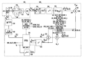
- FIG. 1 is a functional block diagram of the overall architecture of the frequency selective automatic gain control function with dual attack and release times and interference detection;
- FIG. 2 depicts a AGC individual frequency bin loop for a given frequency bin ⁇
- FIG. 3 shows a gain profile derived in accordance with the architecture of FIG. 1 ;
- FIG. 4 depicts a AGC individual frequency bin loop analysis model
- FIG. 5 graphically shows AGC step response with a wide band filter.
- the invention resides primarily in a prescribed novel arrangement of conventional telecommunication circuits and components, and attendant communication control software in an attendant digital signal processor.
- the configuration of such circuits and components and the manner in they are interfaced with the communications control software have, for the most part, been depicted in the drawings by readily understandable functional block diagrams, that contain operational flow processing therein, which show only those specific aspects that are pertinent to the present invention, so as not to obscure the disclosure with details which will be readily apparent to those skilled in the art having the benefit of the description herein.
- the block diagram and associated communication control flow diagrams are primarily intended to show the major components of a preferred embodiment of the invention in convenient functional groupings, whereby the present invention may be more readily understood.
- FIG. 1 is a functional-based block diagram of the overall architecture of the frequency selective automatic gain control function with dual attack and release times in accordance with a preferred embodiment of the present invention.
- the invention includes a front-end hardware section 100 through which a signal is received, and an associated digital processor-resident software section 200 , to which the output of the hardware section is coupled, and which is used to control the gain of a variable gain stage 110 of the hardware section in accordance with a multifrequency bin-based gain profile developed by the software section in the course of its analysis of the energy in the various frequency bins to which the receiver hops.
- the aggregate input signal r(t) is coupled to a software controlled variable gain stage 110 , the output of which is coupled through a splitter/divider 120 to a wideband filter stage 130 and to a narrowband filter stage 140 , in this non-limiting example.
- the use of the two filters in the figure is necessary for the system in which the receiver is used and is not relevant to present invention other than the filter selected for a particular system configuration acts as an anti-aliasing filter.
- the output of one of these stages is selected by way of a selection switch 150 and is coupled to the input of ADC 160 .
- the digital quantity produced by ADC 160 corresponds to the received signal r(n) multiplied by a prescribed gain quantity G k (lk) supplied to the variable gain stage 110 from the gain profile-generating software section 200 .
- the power in this signal sample representation is derived in power calculation block 210 , which derives the quantity:
- This quantity is delayed in a delay block 220 to account for propagation delay in the execution of operations in the digital signal processor, to be described, and then converted into logarithmic format in a log base 10 conversion stage 230 , to produce a measured and gain adjusted signal energy quantity P issi (ik ⁇ D) (k ⁇ D), which is supplied in turn to an inverting ( ⁇ ) input 241 of summation operator 240 , to the non-inverting (+) input 242 of which is supplied the optimal loading factor LF opt .
- the AGC algorithm is frequency selective, and adapts to different aggregate input signal conditions in a prescribed number of frequency bins (such as 32 bins as a non-limiting example, as shown in FIG. 2 .
- the frequency bin for a given hop is based on the hop's center frequency.
- the AGC function initializes and starts the AGC frequency selective mechanism with a pre-determined initial gain profile.
- the AGC mechanism of the present invention is a frequency selective, dual bandwidth, first order, automatic gain control loop.
- the respective components of the AGC mechanism are shown in FIG. 1 and run a dual bandwidth AGC loop in each of up to 32 frequency bins in the present example, with each frequency bin AGC_Bin corresponding to a range of frequencies the systems operating band. Due to the random frequency hopping on the downlink, the frequency bin sampling period is random.
- the digital signal processing entity calculates a 16-bit input signal strength indicator (ISSI) value as
- the gain setting (in dB), g k (lk) , for that frequency bin is looked up in the current gain profile vector GP(k) 250 , and quantized to a 0.5 dB step size by 0.5 dB Quantizer operator 260 . It should be noted that the gain profile vector is stored in an unquantized, floating point format to avoid setting an upper limit on the AGC's attack/release time.
- the loading factor is defined as the ratio of the average power of the aggregate input signal to the power of a sine wave with an amplitude equal to the ADC's full scale.
- the loading factor LF opt is determined via analysis based on analysis to be the loading factor that optimizes the effects of quantization on the incoming desired signal. For a 10-bit ADC, a full scale sine wave will result in an ISSI measurement of 32,640 which is approximated as 2 15 in equation (4).
- the gain error from summation operator 270 is then used to update the gain profile value for the corresponding frequency bin as shown in FIG. 1 .
- the loading factor is defined as the ratio of the average power of the aggregate input signal to the power of a sine wave with it's amplitude equal to the ADC's full scale. If an ADC is underloaded, the digital demodulator's ADC quantization noise can degrade the terminals G/T.
- the loading factor is selected such that the AWGN noise density at the input to the ADC is increased by no more than an amount determined during the demodulator implementation loss budget allocation process.
- ⁇ denotes the ceiling function
- ⁇ No is the allowable noise density increase
- Neq_BW is the noise equivalent bandwidth.
- the 6 dB in equation (5) serves to account for the maximum peak-to-peak receive-chain gain variation.
- a determination of the loop parameter is discussed below.
- an out of range (OOR) fault high is set by the gain profile vector operator 250 and the gain is clipped to the minimum allowable value. This fault is considered a minor fault.
- the new gain is greater than the max gain, MAX_GAIN_S, the gain is clipped to MAX_GAIN_S. It may be noted that MAX_GAIN_S is often selected to be the required gain to get the minimum input noise only power to LF opt .
- the out of range low fault is handled in conjunction with the large gain error detection discussed below.
- the primary AGC loop bandwidth, and thus the attack and release times, are set by the loop parameter K p — S, which is supplied to gain error multiplier 280 .
- the loop updates for a given frequency bin at random time intervals due to the frequency hopping nature of the downlink.
- the attack and release times are random variables that are functions of the probability of visiting a given frequency bin on a given hop and the hopping period.
- a secondary gain adjustment mechanism is included in the AGC mechanism.
- the functional operator 290 labeled “Large Gain Error Detection & OOR Low Error Detection” in FIG. 1 performs a large gain error (LGE) handing technique that effectively adapts the AGC's loop bandwidth when large gain errors are detected.
- LGE large gain error
- the LGE technique permits setting different thresholds for low or high gain errors—thus permitting the LGE attack and releases times to be set differently.
- the input signal strength is continuously checked against a minimum signal level threshold set by the receiver's noise floor.
- This out of range (OOR) low fault is detected using the same period as the LGE detector, but also uses the current gain setting for the corresponding frequency bin in the detection.
- the Hop_Valid flag indicates an ISSI value corresponding to a hop in which the terminal expected a “valid hop” and is used to weight valid hops when determining a high large gain error condition exists, which resets the LGE low error counters for a used hop.
- the AGC gross interference detection algorithm uses the maximum gain variation between any two frequency bins to detect the presence of such an interferer.
- the AGC function reports a gross downlink interference fault with a center frequency estimate of the band in which the interferer lies. It may be noted that the accuracy of the gross interferer's center frequency is a function of the analog anti-aliasing filter being used and is accurate to approximately half the noise equivalent bandwidth of this filter.
- the AGC release time T rls and attack time T atk are defined to be the time for the AGC loop in a given frequency bin to settle to within ⁇ 1 dB of final value after a step in input power in that bin of ⁇ 10 dB, respectively. It is intended that the AGC not track input signal variations due to scintillation; therefore, the AGC mean attack and release times need to be 10 times the max scintillation decorrelation time max( ⁇ o ), thus allowing the AGC loop filter to ignore signal variations due to scintillation. To set the attack/release time the AGC loop's step response and mean time between observations must be determined.
- the AGC loop is shown in FIG. 2 for a given frequency bin ⁇ of a plurality of frequency bins such as the 32 bin gain profile of the present example shown in FIG. 3 .
- This new input is simply a shifted version of P in ( ⁇ ) (m); thus, a ⁇ 10 dB step in P in ( ⁇ ) (m) equates to a ⁇ 10 dB step in P ⁇ in ( ⁇ ) (m).
- the attack/release times then become the time for the gain error E gain ( ⁇ ) (m) to decay to ⁇ 1 dB after a step of ⁇ 10 dB step in P ⁇ in ( ⁇ ) (m).
- H AGC ( z ) ( z ⁇ 1 ⁇ 1)/(1 ⁇ z ⁇ 1 +K p — Sz ⁇ D )
- the sample interval, or time between observations, T AGC for a given frequency bin is random, so that the attack/release times are random.
- the objective is to set the mean attack/release time to be 10*max ( ⁇ o ).
- T hop is the hopping interval. From pg 7, equation 0.231.2, of the textbook by Gradshteyn & Ryzhik, entitled “Tables of Integrals, Series, and Products”, Academic Press, 1980, the above equation converts to:
- the step response for the AGC in a given frequency bin is plotted in FIGS. 5 and 6 for different values of K P — S and D as a function of time, normalized by T hop /max( ⁇ o ).
- the loop delay is limited by the collection/processing epoch of the present example to 32 hop interval. It can be expected that the DSP processing will take less than 32 hop intervals to complete; therefore, if every hop were to be in a given frequency bin, the delay could be as much as 2*32 or 64 hop intervals.
- the large gain error (LGE) handling function of the AGC mechanism of FIG. 1 adapts the loop's attack/release time when gain errors that exceed the LGE_high_S and LGE_low_S thresholds. These are set to ⁇ 10 dB to handle gain errors that prevent the magnitude of the gain error from being greater than 1 dB for more than 10 times the max scintillation decorrelation time max( ⁇ o ). To accomplish this, the gain in a frequency bin is adjusted in ⁇ 3 dB steps when a large gain error is “detected”. LGE detection is based on level crossings with the detection estimation period set by LGE_cnt_mod_S to be approximately two frame periods, in expectation.
- the gain error count (high or low) for the corresponding frequency bin is incremented. If the ISSI measurement coincided with a hop that had a known valid hop, and exceeded the LGE high threshold, the LGE high count is incremented by 1 plus LGE_valid_hop_weight_S and the LGE low counts are reset to 0. Once the LGE high or low count for a frequency bin exceeds the LGE_error_cnt_low_max_S or LGE_error_cnt_high_max_S in a frequency bin, the bin's gain is adjusted by ⁇ 3 dB and the counts for that bin are reset. Every LGE_cnt_mod_S counts, all counters are reset if neither the LGE_error_cnt_low_max_S nor the LGE_error_cnt_high_max_S count is exceeded.
- LGE_error_cnt_high_max_S or LGE_error_cnt_low_max_S is set to a value greater than LGE_cnt_mod_S.
- the out-of-range (OOR) low detection function 290 is used to determine when the aggregate input is below acceptable levels.
- the threshold is used in conjunction by the LGE low detection algorithm, with OOR_Low_threshold_S threshold in-lieu of the LGE_low_S threshold for detecting the OOR low fault.
- the parameter min(N o ) is application specific.
- the noise equivalent bandwidth is designated as N eq — BW.
- the 3 dB factor is included to add margin against false alarms.
- a gross interference detection algorithm is executed by gross interference detector 300 , which uses the peak-to-peak gain deviation among frequency bins, to determine if a high power interferer is present in the receive band and makes an estimate of the interferers center frequency.
- FIG. 1 also shows time delays 310 and 320 that ensure time alignment of variables being processed, as well as an exponential operator to convert the log 10 format of the data into that for driving the variable gain stage 110 .
- the peak-to-peak gain deviation threshold CID_threshold_S is set at the maximum peak-to-peak frequency deviation, plus 3 dB.
- the peak-to-peak gain deviation in the gain profile is sampled several times a second, and if the deviation exceeds the threshold, a gross interferer detected fault is set and a frequency estimate is made by centroiding between the frequency bins with the minimum gain.
- the accuracy of the frequency estimate is dependent on the anti-aliasing filter used and is approximately equal to half of the noise equivalent bandwidth of the filter.
Abstract
Description
E gain (lk)(k)=LFopt−10 LOG10(issi(k)/215)
LFopt=┌┐\ADC_No−10 log10(10ΔNo/10−1)+(10 log10(NeqBW)+6 dB)
H AGC(z)=(z −1−1)/(1−z −1 +K p
h AGC step(m)=Z −1[−10/(1−z −1 +K p
p AGC
E[T AGC] =T hop /P AGC
K p
a·OOR_Low_threshold— S=LFopt−min(N o)−10 log10(N eq
E gain (lk)(k)=LFopt−10 LOG10(issi(k)/215)
LFopt=┌\ADC_No−10 log10(10ΔNo/10−1)+10 log10(NeqBW)+6 dB┐÷ (5)
H AGC(z)=(z −1−1)/(1−z −1 +K p
h AGC step(m)=Z −1[−10/(1−z −1 +K p
E[T AGC] =T hop /p AGC
K p
OOR_Low_threshold— S=LFopt−min(N o)−10 log10(N eq
Claims (27)
Priority Applications (1)
| Application Number | Priority Date | Filing Date | Title |
|---|---|---|---|
| US11/243,289 US7830991B2 (en) | 2005-10-03 | 2005-10-03 | Frequency selective automatic gain control with dual non-symmetric attack and release times and interference detection feature |
Applications Claiming Priority (1)
| Application Number | Priority Date | Filing Date | Title |
|---|---|---|---|
| US11/243,289 US7830991B2 (en) | 2005-10-03 | 2005-10-03 | Frequency selective automatic gain control with dual non-symmetric attack and release times and interference detection feature |
Publications (2)
| Publication Number | Publication Date |
|---|---|
| US20070076783A1 US20070076783A1 (en) | 2007-04-05 |
| US7830991B2 true US7830991B2 (en) | 2010-11-09 |
Family
ID=37901902
Family Applications (1)
| Application Number | Title | Priority Date | Filing Date |
|---|---|---|---|
| US11/243,289 Active 2028-06-19 US7830991B2 (en) | 2005-10-03 | 2005-10-03 | Frequency selective automatic gain control with dual non-symmetric attack and release times and interference detection feature |
Country Status (1)
| Country | Link |
|---|---|
| US (1) | US7830991B2 (en) |
Cited By (5)
| Publication number | Priority date | Publication date | Assignee | Title |
|---|---|---|---|---|
| US20120013399A1 (en) * | 2010-07-16 | 2012-01-19 | Novatek Microelectronics Corp. | Automatic gain control circuit and automatic gain control method |
| US8391384B2 (en) | 2006-12-29 | 2013-03-05 | Agere Systems Llc | Multi-channel receiver with improved AGC |
| US9288776B2 (en) | 2013-11-05 | 2016-03-15 | Qualcomm Incorporated | Apparatus and method of wideband automatic gain control algorithm supporting multiple carriers with possibly different air interface technologies |
| US9628217B1 (en) | 2016-09-08 | 2017-04-18 | The United States Of America As Represented By Secretary Of The Navy | Comb limiter combiner with sub-band interference negation |
| CN108307546A (en) * | 2017-08-30 | 2018-07-20 | 北京邮电大学 | A kind of the determination method, apparatus and electronic equipment of target resident state |
Families Citing this family (33)
| Publication number | Priority date | Publication date | Assignee | Title |
|---|---|---|---|---|
| EP2084818B1 (en) * | 2006-11-14 | 2017-03-22 | Nxp B.V. | A method of acquiring a received spread spectrum signal |
| US8036308B2 (en) * | 2007-02-28 | 2011-10-11 | Broadcom Corporation | Method and system for a wideband polar transmitter |
| US7978782B2 (en) * | 2007-02-28 | 2011-07-12 | Broadcom Corporation | Method and system for polar modulation using a direct digital frequency synthesizer |
| US7769357B2 (en) * | 2007-04-25 | 2010-08-03 | Agere Systems Inc. | Multi-channel receiver with improved AGC |
| US7809343B2 (en) | 2007-04-25 | 2010-10-05 | Agere Systems Inc. | Multi-channel receiver with improved AGC |
| WO2009011826A2 (en) * | 2007-07-13 | 2009-01-22 | Dolby Laboratories Licensing Corporation | Time-varying audio-signal level using a time-varying estimated probability density of the level |
| JP4805287B2 (en) * | 2008-02-08 | 2011-11-02 | 株式会社リコー | Wireless communication device |
| US8005152B2 (en) | 2008-05-21 | 2011-08-23 | Samplify Systems, Inc. | Compression of baseband signals in base transceiver systems |
| US8737449B2 (en) * | 2008-09-01 | 2014-05-27 | Nxp, B.V. | Frequency hopping receiver circuit |
| TWI389467B (en) * | 2009-04-08 | 2013-03-11 | Ind Tech Res Inst | Automatic gain control method and apparatus |
| US8588348B2 (en) | 2009-07-10 | 2013-11-19 | Freescale Semiconductor, Inc. | Receiver with automatic gain control |
| US8649388B2 (en) | 2010-09-02 | 2014-02-11 | Integrated Device Technology, Inc. | Transmission of multiprotocol data in a distributed antenna system |
| US9059778B2 (en) * | 2011-01-07 | 2015-06-16 | Integrated Device Technology Inc. | Frequency domain compression in a base transceiver system |
| US8989088B2 (en) * | 2011-01-07 | 2015-03-24 | Integrated Device Technology Inc. | OFDM signal processing in a base transceiver system |
| CN102571137B (en) * | 2012-02-14 | 2013-12-11 | 浙江大学 | Fully-digital direct sequence spread spectrum communication system and rapid pseudo code capturing method thereof |
| US8675789B2 (en) | 2012-04-23 | 2014-03-18 | Cambridge Silicon Radio Limited | Receiver with variable gain elements and automatic gain control to maintain a positive signal to noise ratio margin |
| US9215296B1 (en) | 2012-05-03 | 2015-12-15 | Integrated Device Technology, Inc. | Method and apparatus for efficient radio unit processing in a communication system |
| US9203933B1 (en) | 2013-08-28 | 2015-12-01 | Integrated Device Technology, Inc. | Method and apparatus for efficient data compression in a communication system |
| US9553954B1 (en) | 2013-10-01 | 2017-01-24 | Integrated Device Technology, Inc. | Method and apparatus utilizing packet segment compression parameters for compression in a communication system |
| US9398489B1 (en) | 2013-10-09 | 2016-07-19 | Integrated Device Technology | Method and apparatus for context based data compression in a communication system |
| US8989257B1 (en) | 2013-10-09 | 2015-03-24 | Integrated Device Technology Inc. | Method and apparatus for providing near-zero jitter real-time compression in a communication system |
| US9485688B1 (en) | 2013-10-09 | 2016-11-01 | Integrated Device Technology, Inc. | Method and apparatus for controlling error and identifying bursts in a data compression system |
| US9313300B2 (en) | 2013-11-07 | 2016-04-12 | Integrated Device Technology, Inc. | Methods and apparatuses for a unified compression framework of baseband signals |
| JP6180953B2 (en) * | 2014-02-05 | 2017-08-16 | パナソニック株式会社 | Receiver |
| JP6225041B2 (en) | 2014-02-05 | 2017-11-01 | パナソニック株式会社 | Receiver |
| US9628122B1 (en) * | 2016-07-25 | 2017-04-18 | The Aerospace Corporation | Circuits and methods for reducing interference that spectrally overlaps a desired signal based on dynamic gain control and/or equalization |
| US10056675B1 (en) | 2017-08-10 | 2018-08-21 | The Aerospace Corporation | Systems and methods for reducing directional interference based on adaptive excision and beam repositioning |
| GB201810537D0 (en) * | 2018-06-27 | 2018-08-15 | Nordic Semiconductor Asa | Automatic gain control |
| CN111277349B (en) | 2018-12-04 | 2023-12-22 | 深圳市中兴微电子技术有限公司 | Clock synchronization method and system |
| CN111328113B (en) | 2018-12-14 | 2022-03-25 | 深圳市中兴微电子技术有限公司 | Work frequency point determination method, unmanned aerial vehicle, remote controller, unmanned aerial vehicle system and computer storage medium |
| US11212015B2 (en) | 2020-05-19 | 2021-12-28 | The Aerospace Corporation | Interference suppression using machine learning |
| CN113179237B (en) * | 2021-02-05 | 2024-02-23 | 西安宇飞电子技术有限公司 | Synchronous broadcasting device with frequency jitter |
| CN115276694B (en) * | 2022-09-02 | 2023-05-26 | 中国电子科技集团公司第七研究所 | Frequency hopping receiver and gain automatic control method thereof |
Citations (22)
| Publication number | Priority date | Publication date | Assignee | Title |
|---|---|---|---|---|
| US5029182A (en) | 1988-10-24 | 1991-07-02 | Hughes Aircraft Company | Automatic gain control (AGC) for frequency hopping receiver |
| US5917865A (en) * | 1996-12-31 | 1999-06-29 | Lucent Technologies, Inc. | Digital automatic gain control employing two-stage gain-determination process |
| US6038435A (en) | 1997-12-24 | 2000-03-14 | Nortel Networks Corporation | Variable step-size AGC |
| US20030078011A1 (en) * | 2001-10-18 | 2003-04-24 | Integrated Programmable Communications, Inc. | Method for integrating a plurality of radio systems in a unified transceiver structure and the device of the same |
| US6563891B1 (en) | 1998-11-24 | 2003-05-13 | Telefonaktiebolaget L M Ericsson (Publ) | Automatic gain control for slotted mode operation |
| US20030162518A1 (en) * | 2002-02-22 | 2003-08-28 | Baldwin Keith R. | Rapid acquisition and tracking system for a wireless packet-based communication device |
| US20030161411A1 (en) * | 1997-12-12 | 2003-08-28 | Mccorkle John W. | Ultra wide bandwidth communications method and system |
| US6658069B1 (en) | 1998-06-24 | 2003-12-02 | Nec Corporation | Automatic gain control circuit and control method therefor |
| US6775337B2 (en) * | 2001-08-01 | 2004-08-10 | M/A-Com Private Radio Systems, Inc. | Digital automatic gain control with feedback induced noise suppression |
| US6799023B2 (en) | 1999-02-18 | 2004-09-28 | Nokia Networks Oy | Method of automatic gain control in base station of cellular radio network |
| US6868263B2 (en) | 2002-06-10 | 2005-03-15 | Qualcomm Incorporated | Digital automatic gain control |
| US20050130615A1 (en) * | 2002-03-25 | 2005-06-16 | Hooman Darabi | Programmable gain amplifier (PGA) with AGC in receiver section |
| US20050215258A1 (en) * | 2004-03-25 | 2005-09-29 | Advanced Micro Devices, Inc. | Rate dependent transmission gain control for WLAN systems |
| US7027530B2 (en) * | 2001-04-11 | 2006-04-11 | Atheros Communications, Inc. | Method and apparatus for maximizing receiver performance utilizing mid-packet gain changes |
| US20060120435A1 (en) * | 2004-12-03 | 2006-06-08 | Manfred Punzenberger | Fast frequency-hopping transceiver and method |
| US20060170499A1 (en) * | 2005-01-31 | 2006-08-03 | Freescale Semicondutor, Inc. | Closed loop power control with high dynamic range |
| US20070053451A1 (en) * | 2005-09-02 | 2007-03-08 | Sigma Designs, Inc. | Digital automatic gain control with parallel/serial interface for multiple antenna ultra wideband ofdm system |
| US20070058739A1 (en) * | 2005-08-18 | 2007-03-15 | Turgut Aytur | Automatic gain control for frequency-hopped OFDM |
| US20070076827A1 (en) * | 2005-09-30 | 2007-04-05 | Beamish Norman J | Radio frequency (RF) receiver with double loop integrated fast response automatic gain control (AGC) |
| US7304969B2 (en) * | 2001-03-19 | 2007-12-04 | Cisco Technology, Inc. | Automatic gain control and low power start-of-packet detection for a wireless LAN receiver |
| US7366490B2 (en) * | 2004-11-02 | 2008-04-29 | Northrop Grumman Corporation | Automatic gain control with gain stepping and regulation |
| US7450907B2 (en) * | 2002-03-07 | 2008-11-11 | Nokia Corporation | Power control device and method for calibrating the power of a transmitter or receiver in a mobile communication network |
Family Cites Families (5)
| Publication number | Priority date | Publication date | Assignee | Title |
|---|---|---|---|---|
| SE419581B (en) * | 1980-09-12 | 1981-08-10 | Ericsson Telefon Ab L M | DEVICE IN A RADAR SYSTEM FOR CORRECTION OF PHASE AND AMPLIT ERRORS WHICH APPEAR IN THE SQUARE DETECTOR |
| US4729110A (en) * | 1984-12-24 | 1988-03-01 | General Electric Company | Correction of offset and gain errors in RF receivers |
| EP0948128B1 (en) * | 1998-04-03 | 2004-12-01 | Motorola Semiconducteurs S.A. | DC offset cancellation in a quadrature receiver |
| US20020097812A1 (en) * | 2000-12-01 | 2002-07-25 | John Wiss | In-phase and quadrature-phase rebalancer |
| US7212797B2 (en) * | 2002-04-26 | 2007-05-01 | Qualcomm Incorporated | DC removal techniques for wireless networking |
-
2005
- 2005-10-03 US US11/243,289 patent/US7830991B2/en active Active
Patent Citations (22)
| Publication number | Priority date | Publication date | Assignee | Title |
|---|---|---|---|---|
| US5029182A (en) | 1988-10-24 | 1991-07-02 | Hughes Aircraft Company | Automatic gain control (AGC) for frequency hopping receiver |
| US5917865A (en) * | 1996-12-31 | 1999-06-29 | Lucent Technologies, Inc. | Digital automatic gain control employing two-stage gain-determination process |
| US20030161411A1 (en) * | 1997-12-12 | 2003-08-28 | Mccorkle John W. | Ultra wide bandwidth communications method and system |
| US6038435A (en) | 1997-12-24 | 2000-03-14 | Nortel Networks Corporation | Variable step-size AGC |
| US6658069B1 (en) | 1998-06-24 | 2003-12-02 | Nec Corporation | Automatic gain control circuit and control method therefor |
| US6563891B1 (en) | 1998-11-24 | 2003-05-13 | Telefonaktiebolaget L M Ericsson (Publ) | Automatic gain control for slotted mode operation |
| US6799023B2 (en) | 1999-02-18 | 2004-09-28 | Nokia Networks Oy | Method of automatic gain control in base station of cellular radio network |
| US7304969B2 (en) * | 2001-03-19 | 2007-12-04 | Cisco Technology, Inc. | Automatic gain control and low power start-of-packet detection for a wireless LAN receiver |
| US7027530B2 (en) * | 2001-04-11 | 2006-04-11 | Atheros Communications, Inc. | Method and apparatus for maximizing receiver performance utilizing mid-packet gain changes |
| US6775337B2 (en) * | 2001-08-01 | 2004-08-10 | M/A-Com Private Radio Systems, Inc. | Digital automatic gain control with feedback induced noise suppression |
| US20030078011A1 (en) * | 2001-10-18 | 2003-04-24 | Integrated Programmable Communications, Inc. | Method for integrating a plurality of radio systems in a unified transceiver structure and the device of the same |
| US20030162518A1 (en) * | 2002-02-22 | 2003-08-28 | Baldwin Keith R. | Rapid acquisition and tracking system for a wireless packet-based communication device |
| US7450907B2 (en) * | 2002-03-07 | 2008-11-11 | Nokia Corporation | Power control device and method for calibrating the power of a transmitter or receiver in a mobile communication network |
| US20050130615A1 (en) * | 2002-03-25 | 2005-06-16 | Hooman Darabi | Programmable gain amplifier (PGA) with AGC in receiver section |
| US6868263B2 (en) | 2002-06-10 | 2005-03-15 | Qualcomm Incorporated | Digital automatic gain control |
| US20050215258A1 (en) * | 2004-03-25 | 2005-09-29 | Advanced Micro Devices, Inc. | Rate dependent transmission gain control for WLAN systems |
| US7366490B2 (en) * | 2004-11-02 | 2008-04-29 | Northrop Grumman Corporation | Automatic gain control with gain stepping and regulation |
| US20060120435A1 (en) * | 2004-12-03 | 2006-06-08 | Manfred Punzenberger | Fast frequency-hopping transceiver and method |
| US20060170499A1 (en) * | 2005-01-31 | 2006-08-03 | Freescale Semicondutor, Inc. | Closed loop power control with high dynamic range |
| US20070058739A1 (en) * | 2005-08-18 | 2007-03-15 | Turgut Aytur | Automatic gain control for frequency-hopped OFDM |
| US20070053451A1 (en) * | 2005-09-02 | 2007-03-08 | Sigma Designs, Inc. | Digital automatic gain control with parallel/serial interface for multiple antenna ultra wideband ofdm system |
| US20070076827A1 (en) * | 2005-09-30 | 2007-04-05 | Beamish Norman J | Radio frequency (RF) receiver with double loop integrated fast response automatic gain control (AGC) |
Non-Patent Citations (1)
| Title |
|---|
| Gradshteyn & Ryzhik, "Tables of Integrals, Series, And Products", Texbook, Academic Press, 1980, p. 7. |
Cited By (7)
| Publication number | Priority date | Publication date | Assignee | Title |
|---|---|---|---|---|
| US8391384B2 (en) | 2006-12-29 | 2013-03-05 | Agere Systems Llc | Multi-channel receiver with improved AGC |
| US20120013399A1 (en) * | 2010-07-16 | 2012-01-19 | Novatek Microelectronics Corp. | Automatic gain control circuit and automatic gain control method |
| US8744392B2 (en) * | 2010-07-16 | 2014-06-03 | Novatek Microelectronics Corp. | Automatic gain control circuit and automatic gain control method |
| US9288776B2 (en) | 2013-11-05 | 2016-03-15 | Qualcomm Incorporated | Apparatus and method of wideband automatic gain control algorithm supporting multiple carriers with possibly different air interface technologies |
| US9628217B1 (en) | 2016-09-08 | 2017-04-18 | The United States Of America As Represented By Secretary Of The Navy | Comb limiter combiner with sub-band interference negation |
| CN108307546A (en) * | 2017-08-30 | 2018-07-20 | 北京邮电大学 | A kind of the determination method, apparatus and electronic equipment of target resident state |
| CN108307546B (en) * | 2017-08-30 | 2020-09-25 | 北京邮电大学 | Method and device for determining target residence state and electronic equipment |
Also Published As
| Publication number | Publication date |
|---|---|
| US20070076783A1 (en) | 2007-04-05 |
Similar Documents
| Publication | Publication Date | Title |
|---|---|---|
| US7830991B2 (en) | Frequency selective automatic gain control with dual non-symmetric attack and release times and interference detection feature | |
| US6721547B2 (en) | In-band and out-of-band signal detection for automatic gain calibration systems | |
| US7643810B2 (en) | Method and system for noise floor calibration and receive signal strength detection | |
| US8964913B1 (en) | Apparatus and method for selecting antennas based on peak-to-average ratios of received signals | |
| US7536159B2 (en) | Automatic gain control using signal and interference power to obtain extended blocking performance | |
| US7046749B2 (en) | Narrowband gain control of receiver with digital post filtering | |
| US7463704B1 (en) | Multi-chain signal detection and gain control for automatic gain control systems | |
| EP1784660B1 (en) | Radar protection device for wireless networks | |
| US7835687B2 (en) | Jamming detector and jamming detecting method | |
| US6785523B2 (en) | Self-correlation detection in automatic gain calibration | |
| US4638493A (en) | Adaptive interference rejection for improved frequency hop detection | |
| US7522556B2 (en) | Signal recognition in an on-frequency repeater | |
| US7535978B2 (en) | Accurate signal detection in a wireless environment | |
| KR19980071390A (en) | Apparatus and method for detection and reduction of intermodulation deformation | |
| US10462757B2 (en) | Automatic gain control based on signal spectrum sensing | |
| US5465405A (en) | Apparatus and method for detecting signals | |
| WO1994026036A1 (en) | Apparatus and method for substantially eliminating noise in an audible output signal | |
| EP1147615B1 (en) | A homodyne radio receiver | |
| US6671504B1 (en) | Radio squelch techniques | |
| US7979041B1 (en) | Out-of-channel received signal strength indication (RSSI) for RF front end | |
| US20080039041A1 (en) | Method and apparatus for reducing inter-modulation | |
| US6771721B1 (en) | Method and apparatus for eliminating audio clicks in a radio receiver | |
| WO2002091104A2 (en) | Self-correlation detection and in-band and out-of-band signal detection for automatic gain calibration systems | |
| US20060034351A1 (en) | Monitoring stability of an on-frequency repeater | |
| MXPA02007493A (en) | System for continuous wave rejection. |
Legal Events
| Date | Code | Title | Description |
|---|---|---|---|
| AS | Assignment |
Owner name: HARRIS CORPORATION, FLORIDA Free format text: ASSIGNMENT OF ASSIGNORS INTEREST;ASSIGNORS:DISHMAN, JOHN F.;BEADLE, EDWARD R.;REEL/FRAME:017098/0239 Effective date: 20050927 |
|
| STCF | Information on status: patent grant |
Free format text: PATENTED CASE |
|
| FPAY | Fee payment |
Year of fee payment: 4 |
|
| MAFP | Maintenance fee payment |
Free format text: PAYMENT OF MAINTENANCE FEE, 8TH YEAR, LARGE ENTITY (ORIGINAL EVENT CODE: M1552) Year of fee payment: 8 |
|
| MAFP | Maintenance fee payment |
Free format text: PAYMENT OF MAINTENANCE FEE, 12TH YEAR, LARGE ENTITY (ORIGINAL EVENT CODE: M1553); ENTITY STATUS OF PATENT OWNER: LARGE ENTITY Year of fee payment: 12 |