US7826287B2 - Testing non-volatile memory devices for charge leakage - Google Patents
Testing non-volatile memory devices for charge leakage Download PDFInfo
- Publication number
- US7826287B2 US7826287B2 US12/280,480 US28048006A US7826287B2 US 7826287 B2 US7826287 B2 US 7826287B2 US 28048006 A US28048006 A US 28048006A US 7826287 B2 US7826287 B2 US 7826287B2
- Authority
- US
- United States
- Prior art keywords
- testing
- volatile memory
- semiconductor device
- floating gate
- memory semiconductor
- Prior art date
- Legal status (The legal status is an assumption and is not a legal conclusion. Google has not performed a legal analysis and makes no representation as to the accuracy of the status listed.)
- Active, expires
Links
Images


Classifications
-
- G—PHYSICS
- G11—INFORMATION STORAGE
- G11C—STATIC STORES
- G11C29/00—Checking stores for correct operation ; Subsequent repair; Testing stores during standby or offline operation
- G11C29/006—Checking stores for correct operation ; Subsequent repair; Testing stores during standby or offline operation at wafer scale level, i.e. wafer scale integration [WSI]
-
- G—PHYSICS
- G11—INFORMATION STORAGE
- G11C—STATIC STORES
- G11C29/00—Checking stores for correct operation ; Subsequent repair; Testing stores during standby or offline operation
- G11C29/04—Detection or location of defective memory elements, e.g. cell constructio details, timing of test signals
- G11C29/50—Marginal testing, e.g. race, voltage or current testing
Definitions
- This invention relates to non-volatile memory devices of the kind storing data in the form of electrical charge in cells in semiconductor dice. More particularly, the invention relates to testing such devices for charge leakage and to a method of producing devices including such a test.
- Non-volatile memory (‘NVM’) devices store data even when external power supplies are disconnected.
- NVM Non-volatile memory
- Various physical properties of materials have been proposed for data retention.
- the present invention relates to the kind of NVM devices in which electrical charge is retained in cells in a semiconductor device and the presence or absence of charge in a cell defines the assertion and de-assertion of a bit of data in the memory.
- a particular kind of NVM device to which the invention is applicable especially, but not exclusively, is a floating gate Metal Oxide Silicon (‘MOS’) device.
- MOS floating gate Metal Oxide Silicon
- Such a device as shown in FIGS. 1 , 2 and 3 of the accompanying drawings comprises a floating gate 12 , typically of polycrystalline Silicon, insulated from the substrate by a layer of Silicon Oxide 16 (although other insulating materials can be used) and forming a lateral Field-Effect Transistor (‘FET’) with source 18 and drain 20 regions under the face of the substrate.
- FET Field-Effect Transistor
- charge is stored in the floating gate to assert or de-assert data stored in the cell by applying an electric potential to a control gate electrode 22 connected to control gate region 24 in capacitive coupling with the floating gate 12 , source 18 , drain 20 and transistor region 26 being grounded and the charge tunnelling through the insulating material between the floating gate 12 on one hand and transistor region 26 on the other hand.
- Data is read by applying a smaller sense potential to the control gate, insufficient to cause significant amounts of charge to tunnel between the floating gate 12 on one hand and the control gate region 24 or transistor region 26 on the other hand, but such as to accumulate greater or lesser amount of charge in the channel of the transistor according to the charge stored in the floating gate 12 .
- the data is then read by responding to the corresponding current flow between the source 18 and drain 20 of the transistor.
- a critical criterion for performance of the NVM device is that the leakage of charge from the cells must be very low, so that charge remains in the cells for the required life. This criterion is to be met by substantially all active cells in the device, even if a small proportion of individual defective cells could be tolerated if data is stored in redundant fashion and error checking algorithms are used.
- Manufacturing techniques do not guarantee a sufficiently high proportion of reliable cells. Accordingly it is necessary to test the charge retention of cells in such a device for defective cells.
- One test technique consists of entering a known data pattern into the device, leaving the device for a period and checking whether each cell has retained the stored data.
- performing this test technique at or near to room temperature requires a test time comparable with the order of magnitude of the required storage life, which is months or even years and is clearly incompatible with testing each dice of a commercial production run or even samples from each production run.
- Test techniques have been proposed in attempts to accelerate obtaining the results.
- One such technique consists of heating the products to be tested.
- temperatures that can be used, in particular because heating to too high a temperature has the effect of permanently altering the physical properties of the products being tested.
- heating may alter the detection of defects by annealing the material of the device under test, which may occur above approximately 125° C. with silicon semiconductor dice and this effect limits the usable temperatures. Accordingly, this technique still requires testing over periods of the order of hundreds of hours or even a thousand hours, which is still highly undesirable for testing whole production runs.
- Another technique utilises the application of an electrical bias to the products to be tested to accelerate charge loss.
- the bias voltage is not effective with all cases of cells liable to charge loss, with the consequent risk of defective cells being undetected and the products shipped to customers, with corresponding degradation of production quality.
- Even combining the technique of heating the tested products with the application of an electrical bias does not solve the problem of quality assurance associated with the electrical bias technique, nor appreciably improve the test time for the heating technique.
- U.S. Pat. No. 5,519,334 discloses a method of characterising charge traps in oxides using a light source.
- U.S. Pat. No. 6,541,987 discloses a method of laser excited detection of defective semiconductor devices.
- Other descriptions of test techniques appear in JEDEC standards: JESD22-A103-B August 2001“High temperature storage life” and JESD22-A117 “EEPROM Program/Erase endurance and data retention” and in the article “Evaluation of EEPROM data retention by field acceleration”, M. Lanzoni, C. Riva, P. Olivo and B. Riccó, Quality and Reliability Engineering International vo 7, 1991.
- the present invention provides a method of testing a non-volatile memory semiconductor device, a method of producing non-volatile memory semiconductor device including such a testing step, and apparatus for testing a non-volatile memory semiconductor device as described in the accompanying claims.
- FIG. 1 is a schematic view in plan of a non-volatile memory device suitable for testing in accordance with one embodiment of the invention, given by way of example,
- FIG. 2 is a schematic sectional view of the NVM device of FIG. 1 along the lines A-A of FIG. 1 ,
- FIG. 3 is a schematic sectional view of the NVM device of FIG. 1 along the lines B-B of FIG. 1 ,
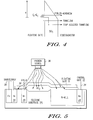
- FIG. 4 is a schematic diagram illustrating some possible mechanisms of charge leakage from the non-volatile memory device of FIG. 1 ,
- FIG. 5 is a schematic view partly in section of a non-volatile memory device being tested in an apparatus in accordance with one embodiment of the invention, given by way of example,
- FIG. 6 is a flow chart of a method of testing a non-volatile memory device in accordance with one embodiment of the invention, given by way of example, and
- FIG. 7 is a graph showing the variations in potential of different cells during the test of FIG. 6 , compared with their variations in potential during a test in accordance with a previously known method (thermal acceleration).
- the non-volatile memory (‘NVM’) device shown to which this embodiment of a method of test is applicable is a floating gate Metal Oxide Silicon (‘MOS’) non-volatile memory device, although it will be appreciated that the invention can be applied to other materials.
- the device comprises an array of memory cells 10 , of which one is shown in the drawing, each comprising a floating gate 12 , of polycrystalline Silicon, insulated from the Silicon substrate 14 by a layer 16 of Silicon Oxide (although other insulating materials can be used).
- Source and drain regions 18 and 20 under the face of the substrate 14 form with the floating gate 12 a lateral Field-Effect Transistor (‘FET’).
- FET Field-Effect Transistor
- the insulating layer 16 is of reduced thickness between the floating gate 12 and the face of the substrate 14 in the transistor region 26 , so that a channel of opposite conductivity type to the substrate may be formed under the face between the source and drain regions 18 and 20 by carriers attracted by the electrical potential due to charge in the floating gate 12 .
- a control gate electrode 22 is provided at a position spaced from the source and drain regions 18 and 20 and connects with a control gate region 24 underlying the floating gate 12 .
- the control gate region 24 is in capacitive coupling with the floating gate 12 .
- the substrate is formed by suitable manufacturing processes, for example including growing a layer on a Silicon body by epitaxial growth, diffusing dopants into the Silicon and etching regions at the surface of the substrate. It will be appreciated that while the present embodiments of a method of and apparatus for testing NVM devices are applicable to an NVM device of the kind shown, they are also applicable to other NVM devices.
- charge is stored in the floating gate 12 to assert or de-assert data stored in the cell 10 by applying an electric potential to the control gate electrode 22 and region 24 in capacitive coupling with the floating gate, the potential being sufficient to cause the charge to tunnel through the insulating material 16 between the control gate region 24 on one hand and floating gate 12 on the other hand, source 18 , drain 20 of transistor region 26 being grounded.
- Data is read by applying a smaller sense potential to the control gate, insufficient to cause significant amounts of charge to tunnel between the floating gate 12 on one hand and transistor region 26 and control gate region 24 on the other hand, but such as to accumulate greater or lesser charge in the channel of the transistor 26 according to the amount of charge stored in the floating gate 12 .
- the data is then read by responding to the corresponding current flow between the source and drain 18 and 20 of the transistor, by applying a potential difference between source and drain.
- the mechanism of leakage of charge, that is to say conduction, away from the floating gate 12 is of the intrinsic type.
- the carriers transit through the insulating material by tunnel effect, directly at low electric fields and by Fowler-Nordheim effect at higher fields.
- the voltage across the insulating layer will be of the order of 5 volts for a charge of 10 ⁇ 13 C and the Fowler-Nordheim effect will predominate.
- the accumulation of charge in the floating gate 12 increases the electric field in the underlying insulating layer thus increasing current conduction through the energy barrier ⁇ of the insulator as shown in FIG. 4 , in which the vertical axis represents energy levels and the horizontal axis represents position in the thickness of the device.
- Faults in the insulating layer give rise to extrinsic mechanisms of charge leakage.
- charge traps which may increase the probability of leakage by the intrinsic mechanism or generate extrinsic mechanisms such as trap-assisted tunneling.
- Heating would energise the charges and increase the chances of the energy of the charge exceeding the barrier ( ) for a given mechanism of tunnelling, accelerating the loss of charge from the floating gate 12 . This is the phenomenon utilised by the standard heating test referred to above. Acceleration of the charge leakage by application of high electric field would also increase the chances of the charge tunnelling through the insulator but would mask and neglect certain types of defect.
- the NVM device is tested systematically after production in an apparatus of which one example is shown in FIG. 5 .
- the apparatus includes probes 30 , 32 and 34 for applying electrical potentials to the source and drain electrodes 18 and 20 and to the control gate electrode 22 and region 24 .
- a processor (not shown) is arranged to apply a test pattern of electrical charges to the floating gates 12 and to compare it to the pattern of charges remaining on the floating gates 12 of the cells 10 after exposure to the radiation, so that any substantial change in the charges remaining on the floating gate 12 of a cell 10 is indicative of defects, as in known test methods.
- the test apparatus also includes a source of electromagnetic radiation 36 , which is chosen so that a photon impacting a charge carrier will energise the carrier and accelerate substantially its chances of leaking from a defective cell.
- the radiation can flood the surface of a wafer including many of the devices to be tested. However in this embodiment of the present invention, the radiation is more focussed and is scanned to cover the surface of the wafer progressively. In manufacturing production of the devices, the test is then carried out on the wafer before separation of the devices from the wafer, in the probe test station. However it is also possible to test individual devices.
- the positions of carriers in the floating gate 12 most likely to give rise to charge leakage are situated close to the interface between the floating gate 12 and the insulating layer 16 . Accordingly, the wavelength of the radiation and the direction of its propagation are chosen to ensure that the radiation penetrates to these positions.
- the radiation illuminates the surface of the cell 10 and passes through the Polysilicon of the floating gate 12 .
- the test has been performed using a variety of wavelengths of radiation in the visible range.
- the Polysilicon is typically highly doped, for example with Boron or Phosphorus. It has been found that in testing a device with this type of Polysilicon, radiation of wavelength in the range of 440 to 560 nm is capable of penetrating the upper layers sufficiently, although radiation of other wavelengths can be used.
- radiation of wavelength in the range of 480 to 520 nm has been found especially effective.
- the above wavelengths have been found effective to excite the charges and accelerate charge loss of defective cells substantially more than charge loss from non-defective cells, whose charge loss during the test time remains negligeable.
- the power density of incident radiation was chosen so as to avoid excessive heating of the device being tested and densities between 5 and 30 mW/cm 2 were found especially effective, although greater or smaller power densities are also effective.
- the density of photons at such power levels gave a very substantial acceleration of the extrinsic leakage mechanisms involved, the chances of a photon intercepting a charge carrier being sufficient even after attenuation of the radiation by the upper layers through which it transits.
- FIG. 7 illustrates a comparison of the test results using a standard heating test (the horizontal axis) and the test of this embodiment of the present invention (the vertical axis). It has been found that the distribution of charge loss from defective cells, measured by the drop in voltage at the floating gate 12 during the course of the tests is extremely similar and the same defective cells were detected by both tests (standard heating test and the radiation test of this embodiment of the present invention). However, the heating test, carried out at 300° C., which cannot be exceeded without a risk of damaging the device tested, took 100 hours, whereas the radiation test of this embodiment of the present invention at wavelength 514.5 nm took 20 mins and the same radiation test at wavelength 488 nm took only 5 mins. Optimisation of the parameters of the radiation test of this embodiment of the present invention is expected to be possible and to improve further the performance of the radiation test.
- the design of the NVM device itself will influence the reliability of the test of the present invention and optimisation of the test parameters will take account of specific aspects, such as the positioning of metal conductors or other layers that could strongly absorb or reflect the test radiation. It is desirable for such layers to avoid the regions above the floating gate 12 in the transistor region 26 and control gate region 24 .
Landscapes
- Testing Or Measuring Of Semiconductors Or The Like (AREA)
- For Increasing The Reliability Of Semiconductor Memories (AREA)
- Testing Of Individual Semiconductor Devices (AREA)
- Non-Volatile Memory (AREA)
Abstract
Description
Claims (20)
Applications Claiming Priority (1)
| Application Number | Priority Date | Filing Date | Title |
|---|---|---|---|
| PCT/EP2006/002854 WO2007095974A1 (en) | 2006-02-24 | 2006-02-24 | Testing non-volatile memory devices for charge leakage |
Publications (2)
| Publication Number | Publication Date |
|---|---|
| US20090016115A1 US20090016115A1 (en) | 2009-01-15 |
| US7826287B2 true US7826287B2 (en) | 2010-11-02 |
Family
ID=36678600
Family Applications (1)
| Application Number | Title | Priority Date | Filing Date |
|---|---|---|---|
| US12/280,480 Active 2026-08-29 US7826287B2 (en) | 2006-02-24 | 2006-02-24 | Testing non-volatile memory devices for charge leakage |
Country Status (3)
| Country | Link |
|---|---|
| US (1) | US7826287B2 (en) |
| TW (1) | TWI440038B (en) |
| WO (1) | WO2007095974A1 (en) |
Families Citing this family (2)
| Publication number | Priority date | Publication date | Assignee | Title |
|---|---|---|---|---|
| US10978171B2 (en) * | 2019-07-31 | 2021-04-13 | Microsoft Technology Licensing, Llc | Identification of susceptibility to induced charge leakage |
| US11762563B1 (en) * | 2021-01-28 | 2023-09-19 | Board Of Trustees Of The University Of Alabama, For And On Behalf Of The University Of Alabama In Huntsville | Systems and methods for improving radiation tolerance of memory |
Citations (8)
| Publication number | Priority date | Publication date | Assignee | Title |
|---|---|---|---|---|
| US4799021A (en) * | 1986-07-22 | 1989-01-17 | Sgs Microelettronica S.P.A. | Method and apparatus for testing EPROM type semiconductor devices during burn-in |
| US5109257A (en) * | 1988-12-27 | 1992-04-28 | Nec Corporation | Testing circuit for semiconductor memory array |
| US5265099A (en) | 1991-02-28 | 1993-11-23 | Feinstein David Y | Method for heating dynamic memory units whereby |
| US5519334A (en) | 1994-09-29 | 1996-05-21 | Advanced Micro Devices, Inc. | System and method for measuring charge traps within a dielectric layer formed on a semiconductor wafer |
| US5986461A (en) | 1996-09-17 | 1999-11-16 | Intel Corporation | UV methods for screening open circuit defects in CMOS integrated circuits |
| US20020021141A1 (en) | 2000-07-25 | 2002-02-21 | Udo Hartmann | Apparatus for testing semiconductor devices |
| US20030001597A1 (en) | 2001-06-28 | 2003-01-02 | Li-Shen Juhn | Method of testing radiation for a SDRAM |
| US6541987B1 (en) | 1999-08-30 | 2003-04-01 | Advanced Micro Devices, Inc. | Laser-excited detection of defective semiconductor device |
-
2006
- 2006-02-24 US US12/280,480 patent/US7826287B2/en active Active
- 2006-02-24 WO PCT/EP2006/002854 patent/WO2007095974A1/en active Application Filing
-
2007
- 2007-02-16 TW TW096105951A patent/TWI440038B/en not_active IP Right Cessation
Patent Citations (8)
| Publication number | Priority date | Publication date | Assignee | Title |
|---|---|---|---|---|
| US4799021A (en) * | 1986-07-22 | 1989-01-17 | Sgs Microelettronica S.P.A. | Method and apparatus for testing EPROM type semiconductor devices during burn-in |
| US5109257A (en) * | 1988-12-27 | 1992-04-28 | Nec Corporation | Testing circuit for semiconductor memory array |
| US5265099A (en) | 1991-02-28 | 1993-11-23 | Feinstein David Y | Method for heating dynamic memory units whereby |
| US5519334A (en) | 1994-09-29 | 1996-05-21 | Advanced Micro Devices, Inc. | System and method for measuring charge traps within a dielectric layer formed on a semiconductor wafer |
| US5986461A (en) | 1996-09-17 | 1999-11-16 | Intel Corporation | UV methods for screening open circuit defects in CMOS integrated circuits |
| US6541987B1 (en) | 1999-08-30 | 2003-04-01 | Advanced Micro Devices, Inc. | Laser-excited detection of defective semiconductor device |
| US20020021141A1 (en) | 2000-07-25 | 2002-02-21 | Udo Hartmann | Apparatus for testing semiconductor devices |
| US20030001597A1 (en) | 2001-06-28 | 2003-01-02 | Li-Shen Juhn | Method of testing radiation for a SDRAM |
Non-Patent Citations (5)
| Title |
|---|
| Brown, "Telecommunications" T&A Constable, Ltd., 1974, Edinburch XP002391993, p. 5, paragraph 1.4-p. 7, line 18; figure 1.3. |
| JESD22-A103-B, "High Temperature Storage Life", Aug. 2001, 10 pages, JEDEC Solid State Technology Association, USA. |
| JESD22-A117, "EEPROM Program/Erase endurance and data retention", Mar. 2006, 16 pages, JEDEC Solid State Technology Association, USA. |
| Lanzoni, et al. "Evaluation of EEPROM data retention by field acceleration", 1991 Quality and Reliability Engineering Int'l, vol. 7. |
| PCT/EP2006/002854 Search Report and Written Opinion, Aug. 10, 2006. |
Also Published As
| Publication number | Publication date |
|---|---|
| TW200739589A (en) | 2007-10-16 |
| WO2007095974A1 (en) | 2007-08-30 |
| US20090016115A1 (en) | 2009-01-15 |
| TWI440038B (en) | 2014-06-01 |
Similar Documents
| Publication | Publication Date | Title |
|---|---|---|
| US6049213A (en) | Method and system for testing the reliability of gate dielectric films | |
| US6091652A (en) | Testing semiconductor devices for data retention | |
| KR101458350B1 (en) | A method of testing data retention of a non-volatile memory cell having a floating gate | |
| US20030074152A1 (en) | System and method of testing non-volatile memory cells | |
| Tkachev et al. | Floating-gate corner-enhanced poly-to-poly tunneling in split-gate flash memory cells | |
| US20070230261A1 (en) | Nonvolatile semiconductor memory device and method for testing the same | |
| Modelli et al. | A new conduction mechanism for the anomalous cells in thin oxide flash EEPROMs | |
| San et al. | Effects of erase source bias on Flash EPROM device reliability | |
| US5764569A (en) | Test structure and method to characterize charge gain in a non-volatile memory | |
| Manabe et al. | Detailed observation of small leak current in flash memories with thin tunnel oxides | |
| US7826287B2 (en) | Testing non-volatile memory devices for charge leakage | |
| Modelli et al. | Advanced flash memory reliability | |
| Fan et al. | Cryogenic characterisation of 55 nm SONOS charge‐trapping memory in AC and DC modes | |
| Liu et al. | A powerless and non-volatile counterfeit IC detection sensor in a standard logic process based on an exposed floating-gate array | |
| Chimenton et al. | Overerase phenomena: an insight into flash memory reliability | |
| Sikora et al. | Technologies and reliability of modern embedded flash cells | |
| De Nardi et al. | Direct measurements of charge in floating gate transistor channels of flash memories using scanning capacitance microscopy | |
| JP2006127582A (en) | Manufacturing method of semiconductor apparatus | |
| Mohammad et al. | Electrical model for program disturb faults in non-volatile memories | |
| Yeoh et al. | Novel Nano-probing Technique for Column Short Failure in Flash Memory Devices | |
| Ng et al. | Localization of NVM Inter-Poly Defects using nanoprobing techniques | |
| CN112652352B (en) | Data retention test method of flash memory | |
| Lee et al. | On the scaling of flash cell spacer for gate disturb and charge retention optimization | |
| JP2001266598A (en) | Test method for characteristics of non-volatile semiconductor memory | |
| Zhang et al. | Research on Retention Evaluation Method of Floating Gate Memory Used in Aerospace |
Legal Events
| Date | Code | Title | Description |
|---|---|---|---|
| AS | Assignment |
Owner name: CITIBANK, N.A., NEW YORK Free format text: SECURITY AGREEMENT;ASSIGNOR:FREESCALE SEMICONDUCTOR, INC.;REEL/FRAME:021936/0772 Effective date: 20081107 Owner name: CITIBANK, N.A.,NEW YORK Free format text: SECURITY AGREEMENT;ASSIGNOR:FREESCALE SEMICONDUCTOR, INC.;REEL/FRAME:021936/0772 Effective date: 20081107 |
|
| AS | Assignment |
Owner name: CITIBANK, N.A.,NEW YORK Free format text: SECURITY AGREEMENT;ASSIGNOR:FREESCALE SEMICONDUCTOR, INC.;REEL/FRAME:024085/0001 Effective date: 20100219 Owner name: CITIBANK, N.A., NEW YORK Free format text: SECURITY AGREEMENT;ASSIGNOR:FREESCALE SEMICONDUCTOR, INC.;REEL/FRAME:024085/0001 Effective date: 20100219 |
|
| AS | Assignment |
Owner name: CITIBANK, N.A., AS COLLATERAL AGENT,NEW YORK Free format text: SECURITY AGREEMENT;ASSIGNOR:FREESCALE SEMICONDUCTOR, INC.;REEL/FRAME:024397/0001 Effective date: 20100413 Owner name: CITIBANK, N.A., AS COLLATERAL AGENT, NEW YORK Free format text: SECURITY AGREEMENT;ASSIGNOR:FREESCALE SEMICONDUCTOR, INC.;REEL/FRAME:024397/0001 Effective date: 20100413 |
|
| AS | Assignment |
Owner name: FREESCALE SEMICONDUCTOR, INC., TEXAS Free format text: ASSIGNMENT OF ASSIGNORS INTEREST;ASSIGNORS:MORANCHO MONTAGNER, LAURENCE;CHAPTAL, JEAN LOUIS;DE BORTOLI, SERGE;AND OTHERS;SIGNING DATES FROM 20060301 TO 20060317;REEL/FRAME:024936/0455 |
|
| STCF | Information on status: patent grant |
Free format text: PATENTED CASE |
|
| AS | Assignment |
Owner name: CITIBANK, N.A., AS NOTES COLLATERAL AGENT, NEW YOR Free format text: SECURITY AGREEMENT;ASSIGNOR:FREESCALE SEMICONDUCTOR, INC.;REEL/FRAME:030633/0424 Effective date: 20130521 |
|
| AS | Assignment |
Owner name: CITIBANK, N.A., AS NOTES COLLATERAL AGENT, NEW YOR Free format text: SECURITY AGREEMENT;ASSIGNOR:FREESCALE SEMICONDUCTOR, INC.;REEL/FRAME:031591/0266 Effective date: 20131101 |
|
| FPAY | Fee payment |
Year of fee payment: 4 |
|
| AS | Assignment |
Owner name: FREESCALE SEMICONDUCTOR, INC., TEXAS Free format text: PATENT RELEASE;ASSIGNOR:CITIBANK, N.A., AS COLLATERAL AGENT;REEL/FRAME:037356/0553 Effective date: 20151207 Owner name: FREESCALE SEMICONDUCTOR, INC., TEXAS Free format text: PATENT RELEASE;ASSIGNOR:CITIBANK, N.A., AS COLLATERAL AGENT;REEL/FRAME:037356/0143 Effective date: 20151207 Owner name: FREESCALE SEMICONDUCTOR, INC., TEXAS Free format text: PATENT RELEASE;ASSIGNOR:CITIBANK, N.A., AS COLLATERAL AGENT;REEL/FRAME:037354/0757 Effective date: 20151207 |
|
| AS | Assignment |
Owner name: MORGAN STANLEY SENIOR FUNDING, INC., MARYLAND Free format text: ASSIGNMENT AND ASSUMPTION OF SECURITY INTEREST IN PATENTS;ASSIGNOR:CITIBANK, N.A.;REEL/FRAME:037486/0517 Effective date: 20151207 |
|
| AS | Assignment |
Owner name: MORGAN STANLEY SENIOR FUNDING, INC., MARYLAND Free format text: ASSIGNMENT AND ASSUMPTION OF SECURITY INTEREST IN PATENTS;ASSIGNOR:CITIBANK, N.A.;REEL/FRAME:037518/0292 Effective date: 20151207 |
|
| AS | Assignment |
Owner name: MORGAN STANLEY SENIOR FUNDING, INC., MARYLAND Free format text: SECURITY AGREEMENT SUPPLEMENT;ASSIGNOR:NXP B.V.;REEL/FRAME:038017/0058 Effective date: 20160218 |
|
| AS | Assignment |
Owner name: MORGAN STANLEY SENIOR FUNDING, INC., MARYLAND Free format text: CORRECTIVE ASSIGNMENT TO CORRECT THE REMOVE APPLICATION 12092129 PREVIOUSLY RECORDED ON REEL 038017 FRAME 0058. ASSIGNOR(S) HEREBY CONFIRMS THE SECURITY AGREEMENT SUPPLEMENT;ASSIGNOR:NXP B.V.;REEL/FRAME:039361/0212 Effective date: 20160218 |
|
| AS | Assignment |
Owner name: NXP, B.V., F/K/A FREESCALE SEMICONDUCTOR, INC., NETHERLANDS Free format text: RELEASE BY SECURED PARTY;ASSIGNOR:MORGAN STANLEY SENIOR FUNDING, INC.;REEL/FRAME:040925/0001 Effective date: 20160912 Owner name: NXP, B.V., F/K/A FREESCALE SEMICONDUCTOR, INC., NE Free format text: RELEASE BY SECURED PARTY;ASSIGNOR:MORGAN STANLEY SENIOR FUNDING, INC.;REEL/FRAME:040925/0001 Effective date: 20160912 |
|
| AS | Assignment |
Owner name: NXP B.V., NETHERLANDS Free format text: RELEASE BY SECURED PARTY;ASSIGNOR:MORGAN STANLEY SENIOR FUNDING, INC.;REEL/FRAME:040928/0001 Effective date: 20160622 |
|
| AS | Assignment |
Owner name: NXP USA, INC., TEXAS Free format text: CHANGE OF NAME;ASSIGNOR:FREESCALE SEMICONDUCTOR INC.;REEL/FRAME:040652/0180 Effective date: 20161107 |
|
| AS | Assignment |
Owner name: NXP USA, INC., TEXAS Free format text: CORRECTIVE ASSIGNMENT TO CORRECT THE NATURE OF CONVEYANCE LISTED CHANGE OF NAME SHOULD BE MERGER AND CHANGE PREVIOUSLY RECORDED AT REEL: 040652 FRAME: 0180. ASSIGNOR(S) HEREBY CONFIRMS THE MERGER AND CHANGE OF NAME;ASSIGNOR:FREESCALE SEMICONDUCTOR INC.;REEL/FRAME:041354/0148 Effective date: 20161107 |
|
| AS | Assignment |
Owner name: MORGAN STANLEY SENIOR FUNDING, INC., MARYLAND Free format text: CORRECTIVE ASSIGNMENT TO CORRECT THE REMOVE PATENTS 8108266 AND 8062324 AND REPLACE THEM WITH 6108266 AND 8060324 PREVIOUSLY RECORDED ON REEL 037518 FRAME 0292. ASSIGNOR(S) HEREBY CONFIRMS THE ASSIGNMENT AND ASSUMPTION OF SECURITY INTEREST IN PATENTS;ASSIGNOR:CITIBANK, N.A.;REEL/FRAME:041703/0536 Effective date: 20151207 |
|
| AS | Assignment |
Owner name: MORGAN STANLEY SENIOR FUNDING, INC., MARYLAND Free format text: CORRECTIVE ASSIGNMENT TO CORRECT THE REMOVE APPLICATION 12681366 PREVIOUSLY RECORDED ON REEL 039361 FRAME 0212. ASSIGNOR(S) HEREBY CONFIRMS THE SECURITY AGREEMENT SUPPLEMENT;ASSIGNOR:NXP B.V.;REEL/FRAME:042762/0145 Effective date: 20160218 Owner name: MORGAN STANLEY SENIOR FUNDING, INC., MARYLAND Free format text: CORRECTIVE ASSIGNMENT TO CORRECT THE REMOVE APPLICATION 12681366 PREVIOUSLY RECORDED ON REEL 038017 FRAME 0058. ASSIGNOR(S) HEREBY CONFIRMS THE SECURITY AGREEMENT SUPPLEMENT;ASSIGNOR:NXP B.V.;REEL/FRAME:042985/0001 Effective date: 20160218 |
|
| MAFP | Maintenance fee payment |
Free format text: PAYMENT OF MAINTENANCE FEE, 8TH YEAR, LARGE ENTITY (ORIGINAL EVENT CODE: M1552) Year of fee payment: 8 |
|
| AS | Assignment |
Owner name: SHENZHEN XINGUODU TECHNOLOGY CO., LTD., CHINA Free format text: CORRECTIVE ASSIGNMENT TO CORRECT THE TO CORRECT THE APPLICATION NO. FROM 13,883,290 TO 13,833,290 PREVIOUSLY RECORDED ON REEL 041703 FRAME 0536. ASSIGNOR(S) HEREBY CONFIRMS THE THE ASSIGNMENT AND ASSUMPTION OF SECURITYINTEREST IN PATENTS.;ASSIGNOR:MORGAN STANLEY SENIOR FUNDING, INC.;REEL/FRAME:048734/0001 Effective date: 20190217 |
|
| AS | Assignment |
Owner name: NXP B.V., NETHERLANDS Free format text: RELEASE BY SECURED PARTY;ASSIGNOR:MORGAN STANLEY SENIOR FUNDING, INC.;REEL/FRAME:050745/0001 Effective date: 20190903 |
|
| AS | Assignment |
Owner name: MORGAN STANLEY SENIOR FUNDING, INC., MARYLAND Free format text: CORRECTIVE ASSIGNMENT TO CORRECT THE REMOVE APPLICATION 12298143 PREVIOUSLY RECORDED ON REEL 042985 FRAME 0001. ASSIGNOR(S) HEREBY CONFIRMS THE SECURITY AGREEMENT SUPPLEMENT;ASSIGNOR:NXP B.V.;REEL/FRAME:051029/0001 Effective date: 20160218 Owner name: MORGAN STANLEY SENIOR FUNDING, INC., MARYLAND Free format text: CORRECTIVE ASSIGNMENT TO CORRECT THE REMOVE APPLICATION 12298143 PREVIOUSLY RECORDED ON REEL 042762 FRAME 0145. ASSIGNOR(S) HEREBY CONFIRMS THE SECURITY AGREEMENT SUPPLEMENT;ASSIGNOR:NXP B.V.;REEL/FRAME:051145/0184 Effective date: 20160218 Owner name: MORGAN STANLEY SENIOR FUNDING, INC., MARYLAND Free format text: CORRECTIVE ASSIGNMENT TO CORRECT THE REMOVE APPLICATION 12298143 PREVIOUSLY RECORDED ON REEL 039361 FRAME 0212. ASSIGNOR(S) HEREBY CONFIRMS THE SECURITY AGREEMENT SUPPLEMENT;ASSIGNOR:NXP B.V.;REEL/FRAME:051029/0387 Effective date: 20160218 Owner name: MORGAN STANLEY SENIOR FUNDING, INC., MARYLAND Free format text: CORRECTIVE ASSIGNMENT TO CORRECT THE REMOVE APPLICATION12298143 PREVIOUSLY RECORDED ON REEL 039361 FRAME 0212. ASSIGNOR(S) HEREBY CONFIRMS THE SECURITY AGREEMENT SUPPLEMENT;ASSIGNOR:NXP B.V.;REEL/FRAME:051029/0387 Effective date: 20160218 Owner name: MORGAN STANLEY SENIOR FUNDING, INC., MARYLAND Free format text: CORRECTIVE ASSIGNMENT TO CORRECT THE REMOVE APPLICATION12298143 PREVIOUSLY RECORDED ON REEL 042985 FRAME 0001. ASSIGNOR(S) HEREBY CONFIRMS THE SECURITY AGREEMENT SUPPLEMENT;ASSIGNOR:NXP B.V.;REEL/FRAME:051029/0001 Effective date: 20160218 Owner name: MORGAN STANLEY SENIOR FUNDING, INC., MARYLAND Free format text: CORRECTIVE ASSIGNMENT TO CORRECT THE REMOVE APPLICATION 12298143 PREVIOUSLY RECORDED ON REEL 038017 FRAME 0058. ASSIGNOR(S) HEREBY CONFIRMS THE SECURITY AGREEMENT SUPPLEMENT;ASSIGNOR:NXP B.V.;REEL/FRAME:051030/0001 Effective date: 20160218 Owner name: MORGAN STANLEY SENIOR FUNDING, INC., MARYLAND Free format text: CORRECTIVE ASSIGNMENT TO CORRECT THE REMOVE APPLICATION12298143 PREVIOUSLY RECORDED ON REEL 042762 FRAME 0145. ASSIGNOR(S) HEREBY CONFIRMS THE SECURITY AGREEMENT SUPPLEMENT;ASSIGNOR:NXP B.V.;REEL/FRAME:051145/0184 Effective date: 20160218 |
|
| AS | Assignment |
Owner name: MORGAN STANLEY SENIOR FUNDING, INC., MARYLAND Free format text: CORRECTIVE ASSIGNMENT TO CORRECT THE REMOVE APPLICATION11759915 AND REPLACE IT WITH APPLICATION 11759935 PREVIOUSLY RECORDED ON REEL 037486 FRAME 0517. ASSIGNOR(S) HEREBY CONFIRMS THE ASSIGNMENT AND ASSUMPTION OF SECURITYINTEREST IN PATENTS;ASSIGNOR:CITIBANK, N.A.;REEL/FRAME:053547/0421 Effective date: 20151207 |
|
| AS | Assignment |
Owner name: NXP B.V., NETHERLANDS Free format text: CORRECTIVE ASSIGNMENT TO CORRECT THE REMOVEAPPLICATION 11759915 AND REPLACE IT WITH APPLICATION11759935 PREVIOUSLY RECORDED ON REEL 040928 FRAME 0001. ASSIGNOR(S) HEREBY CONFIRMS THE RELEASE OF SECURITYINTEREST;ASSIGNOR:MORGAN STANLEY SENIOR FUNDING, INC.;REEL/FRAME:052915/0001 Effective date: 20160622 |
|
| AS | Assignment |
Owner name: NXP, B.V. F/K/A FREESCALE SEMICONDUCTOR, INC., NETHERLANDS Free format text: CORRECTIVE ASSIGNMENT TO CORRECT THE REMOVEAPPLICATION 11759915 AND REPLACE IT WITH APPLICATION11759935 PREVIOUSLY RECORDED ON REEL 040925 FRAME 0001. ASSIGNOR(S) HEREBY CONFIRMS THE RELEASE OF SECURITYINTEREST;ASSIGNOR:MORGAN STANLEY SENIOR FUNDING, INC.;REEL/FRAME:052917/0001 Effective date: 20160912 |
|
| MAFP | Maintenance fee payment |
Free format text: PAYMENT OF MAINTENANCE FEE, 12TH YEAR, LARGE ENTITY (ORIGINAL EVENT CODE: M1553); ENTITY STATUS OF PATENT OWNER: LARGE ENTITY Year of fee payment: 12 |