US7825882B2 - Dimming method and system thereof - Google Patents
Dimming method and system thereof Download PDFInfo
- Publication number
- US7825882B2 US7825882B2 US11/704,244 US70424407A US7825882B2 US 7825882 B2 US7825882 B2 US 7825882B2 US 70424407 A US70424407 A US 70424407A US 7825882 B2 US7825882 B2 US 7825882B2
- Authority
- US
- United States
- Prior art keywords
- pin
- dimming
- voltage
- dimming control
- common
- Prior art date
- Legal status (The legal status is an assumption and is not a legal conclusion. Google has not performed a legal analysis and makes no representation as to the accuracy of the status listed.)
- Active, expires
Links
- 238000000034 method Methods 0.000 title claims abstract description 29
- 239000003990 capacitor Substances 0.000 claims description 13
- 238000005070 sampling Methods 0.000 claims description 3
- 238000010586 diagram Methods 0.000 description 3
- 230000008901 benefit Effects 0.000 description 2
- 239000013256 coordination polymer Substances 0.000 description 2
- 230000007423 decrease Effects 0.000 description 2
- 230000003247 decreasing effect Effects 0.000 description 2
- 238000004519 manufacturing process Methods 0.000 description 2
- 238000007792 addition Methods 0.000 description 1
- 230000005540 biological transmission Effects 0.000 description 1
- 230000002860 competitive effect Effects 0.000 description 1
- 238000004806 packaging method and process Methods 0.000 description 1
Images


Classifications
-
- H—ELECTRICITY
- H05—ELECTRIC TECHNIQUES NOT OTHERWISE PROVIDED FOR
- H05B—ELECTRIC HEATING; ELECTRIC LIGHT SOURCES NOT OTHERWISE PROVIDED FOR; CIRCUIT ARRANGEMENTS FOR ELECTRIC LIGHT SOURCES, IN GENERAL
- H05B45/00—Circuit arrangements for operating light-emitting diodes [LED]
- H05B45/40—Details of LED load circuits
- H05B45/44—Details of LED load circuits with an active control inside an LED matrix
- H05B45/46—Details of LED load circuits with an active control inside an LED matrix having LEDs disposed in parallel lines
-
- H—ELECTRICITY
- H05—ELECTRIC TECHNIQUES NOT OTHERWISE PROVIDED FOR
- H05B—ELECTRIC HEATING; ELECTRIC LIGHT SOURCES NOT OTHERWISE PROVIDED FOR; CIRCUIT ARRANGEMENTS FOR ELECTRIC LIGHT SOURCES, IN GENERAL
- H05B45/00—Circuit arrangements for operating light-emitting diodes [LED]
- H05B45/30—Driver circuits
- H05B45/37—Converter circuits
- H05B45/3725—Switched mode power supply [SMPS]
-
- G—PHYSICS
- G09—EDUCATION; CRYPTOGRAPHY; DISPLAY; ADVERTISING; SEALS
- G09G—ARRANGEMENTS OR CIRCUITS FOR CONTROL OF INDICATING DEVICES USING STATIC MEANS TO PRESENT VARIABLE INFORMATION
- G09G3/00—Control arrangements or circuits, of interest only in connection with visual indicators other than cathode-ray tubes
- G09G3/20—Control arrangements or circuits, of interest only in connection with visual indicators other than cathode-ray tubes for presentation of an assembly of a number of characters, e.g. a page, by composing the assembly by combination of individual elements arranged in a matrix no fixed position being assigned to or needed to be assigned to the individual characters or partial characters
- G09G3/34—Control arrangements or circuits, of interest only in connection with visual indicators other than cathode-ray tubes for presentation of an assembly of a number of characters, e.g. a page, by composing the assembly by combination of individual elements arranged in a matrix no fixed position being assigned to or needed to be assigned to the individual characters or partial characters by control of light from an independent source
- G09G3/3406—Control of illumination source
-
- Y—GENERAL TAGGING OF NEW TECHNOLOGICAL DEVELOPMENTS; GENERAL TAGGING OF CROSS-SECTIONAL TECHNOLOGIES SPANNING OVER SEVERAL SECTIONS OF THE IPC; TECHNICAL SUBJECTS COVERED BY FORMER USPC CROSS-REFERENCE ART COLLECTIONS [XRACs] AND DIGESTS
- Y02—TECHNOLOGIES OR APPLICATIONS FOR MITIGATION OR ADAPTATION AGAINST CLIMATE CHANGE
- Y02B—CLIMATE CHANGE MITIGATION TECHNOLOGIES RELATED TO BUILDINGS, e.g. HOUSING, HOUSE APPLIANCES OR RELATED END-USER APPLICATIONS
- Y02B20/00—Energy efficient lighting technologies, e.g. halogen lamps or gas discharge lamps
- Y02B20/30—Semiconductor lamps, e.g. solid state lamps [SSL] light emitting diodes [LED] or organic LED [OLED]
Definitions
- the present invention generally relates to a dimming method of Light Emitting Diode (LED). More particularly, the present invention relates to an LED dimming method, which utilizes high impedance node for inputting a dimming control signal but without the usage of an enable pin additionally.
- LED Light Emitting Diode
- LCD panel such as cell phone, PDA, and MP3 player . . . etc.
- the designer chooses not only the preferred sizes of the LCD panel, but also determines the types of the LCD panel and thereafter the power supply and the back-light circuit thereof in accordance with different applications.
- white LED is the most adopted solution to portable consumer electronic products.
- the white LED solution may be categorized into the charge pump solution and the inductance-based solution.
- the charge pump solution is also called switching capacitance solution, which transfers the power from the input terminal to the output terminal by switching the connections between the input terminal with a flying capacitance and between the flying capacitance with the output terminal. The whole switching process is unnecessary of any inductance device.
- charge pump devices occupy less volume and benefit in ease of design—the designer usually has no need to change the architecture of the charge pump driving circuitry but only chooses a proper capacitance device according to different demands, hence the charge pump solution is very popular.
- the LCD panel requires dimming functions.
- the user may want to brighten a cell phone's or a PDA's screen while under dark environment, or lower the brightness of a cell phone and cut the back-light off after idled for a period of time.
- a well-known LED dimming method is Pulse Width Modulation (PWM) dimming technique, in which the LED dimming signal is modulated in PWM signal.
- PWM Pulse Width Modulation
- one of the PWM-based dimming methods adjusts the current flowed into the LED by changing the “duty cycle” of the PWM dimming signal.
- the duty cycle of the PWM dimming signal is 60%
- the current flowed into the LED will be about 60% of the max value, and the brightness of the LED will decrease 60%.
- Another PWM-based dimming method dims the LED by adjusting the pulse numbers of the PWM signal.
- the MAX1574 series white LED controller of the MAXIM INC. decreases the brightness of the driving LED with 10% each time after the controller received a pulse of PWM signal.
- the above-mentioned two types of dimming methods are the most popular, even if they are a little different, but they both use PWM signal to dim LED.
- FIG. 1 demonstrates a conventional LED driving circuit based on charge pump solution.
- the LED driving IC 10 includes a charge pump 12 , a chip enable/dimming control module 14 and a current sink 16 .
- the pin CP and CN of the LED driving IC 10 are connected to a transfer-capacitor (fly capacitor) Cf, which couples the electric current from the input terminal VIN to the output terminal VOUT for driving LEDs.
- the current sink 16 controls and provides stable current flowed through the LEDs while there are no external dimming signals.
- the chip enable/dimming control module 14 receives dimming control signals from the chip-enable pin EN to control the ON/OFF of the charge pump 12 and the current sink 16 , thereby achieving the main object of the LED driving circuit: control the current flowed through the LEDs and then dim the LEDs.
- an object of the present invention is to provide a dimming method, which is capable of receiving dimming control signals without any single input pin.
- the present LED driving IC does not need any single pin particularly used to receive dimming control signals, therefore the pin's numbers, the package size and the manufacturing cost of the IC could be reduced accordingly.
- the present invention proposes a dimming method applied to driving LED, which receives dimming control signals by utilizing a pin with the other signals in common.
- the present dimming method includes the steps of: every a period of time, floating the pin for an inputted dimming control signal pulling the voltage of the pin up and having the same potential; sampling the voltage of the pin; and restoring the dimming control signal according to the sampled voltage.
- the dimming control signal is pulse width modulated signal
- the step to float the pin is accomplished by temporally switching the pin as a high impedance node.
- FIG. 1 demonstrates a conventional white LED driving circuit based on charge pump solution
- FIG. 2 demonstrates an LED driving circuit with a preferred embodiment of the present invention
- FIG. 3A is the simple diagram of a charge pump
- FIG. 3B shows the timing relationship of the switching signal of a charge pump
- FIG. 4A depicts the connection relationships between the charge pump 22 and the inputted dimming control signal
- FIG. 4B depicts the timing diagram of the circuitry shown in FIG. 4A ;
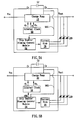
- FIG. 5A depicts an embodiment LED driving circuit with the present LED driving IC of the invention.
- FIG. 5B depicts another embodiment LED driving circuit with the present LED driving IC of the invention
- FIG. 2 demonstrates an LED driving circuit with a preferred embodiment of the present invention.
- the present LED driving IC 20 excludes a chip-enable pin EN.
- the dimming control signals generated from the General Purpose Input/Output (GPIO) module 28 are firstly inputted to the pin CN of the charge pump 22 , and then transferred to the chip-enable/dimming control module 24 .
- the pin CN replaces the original chip-enable pin EN and becomes the input node for receiving dimming control signals.
- FIG. 3A depicts a simple diagram of a charge pump.
- switches 30 and 32 that controlled by two non-overlapped switching signals ⁇ 1 and ⁇ 2 (referring to FIG. 3B ), wherein each set of switches are closed while the switching signals ( ⁇ 1 or ⁇ 2 ) change to high level.
- the switching signal ⁇ 1 changes to high
- the first set of switches 30 are closed and the second set of switches 32 are open, therefore an external power source across the Vin and the GND terminal may charge the capacitor C.
- the switching signals ⁇ 2 changes to high (the switching signal ⁇ 1 stays low)
- the first set of switches 30 are opened and the second set of switches 32 are closed, therefore the capacitor C discharges to the Vout terminal to drive loads (for example, the LEDs).
- the frequencies of the switching signals ⁇ 1 and ⁇ 2 are scaled in MHz, and the charge pump couples current from the input terminal Vin to the output terminal Vout by continuing switching the connections of the capacitor C.
- the charge pump 22 and the transfer capacitor Cf shown in FIG. 2 could be implemented by the charge pump shown in FIG. 3A .
- dimming control signals are inputted through the pin CN and then transferred to the chip-enable/dimming control module 24 , and the chip-enable/dimming control module 24 detects voltage of the pin CN to retrieve the dimming control signals.
- the resistor R is used to limit the current outputted from the GPIO 28 .
- the pin CN Since the GPIO 28 has smaller current-driving force than the external power source, the pin CN is responsive of the across voltage of the transfer capacitor Cf as under normal operation of the charge pump 22 . Hence, the chip-enable/dimming control module 24 could not detect and sample the inputted dimming control signals directly.
- a method is proposed in the present invention. Referring to FIG. 4A , by temporally opening the switches 40 and 42 , the pin CN will be floated and therefore be responsive of the inputted dimming control signals.
- FIG. 4B depicts the timing relationship between of the circuitry shown in FIG. 4A .
- a checking signal chk is generated periodically, which could stop the switching signal ⁇ 1 and ⁇ 2 for one or several time interval.
- the chip-enable/dimming control module 24 detects and samples the voltage of the pin CN, and therefore retrieves the dimming control signals inputted from the GPIO 28 .
- the checking signal chk could be generated by the chip-enable/dimming control module 24 or an internal clock (not shown in the drawing) of the driving IC 20 , and it's not limited in the present invention.
- the sampled dimming control signals are closer to the original signal waveform, so that the chip-enable/dimming control module 24 could control the current sink 26 or ON/OFF of the driving IC 20 itself for dimming the LEDs accordingly.
- FIG. 5A depicts an embodiment LED driving circuit that applies the present invention which includes: a charge pump 22 , a chip-enable/dimming control module 24 and an internal clock 58 , wherein the pin CN is directly connected to the chip-enable/dimming control module 24 by reference to the transmission line 562 .
- the internal clock 58 also generates the checking signal chk for periodically stopping the switching signals ⁇ 1 and ⁇ 2 .
- the checking signal chk could be generated by the chip-enable/dimming control module 24 instead, as well as the previous descriptions. While applying the LED driving IC of FIG. 5A or 5 B to the LED driving circuit shown in FIG. 2 , the dimming control signals could be inputted through the pin CN directly.
- the method temporally switches a specific pin of the driving IC to high impedance, by which the GPIO pulls the voltage of the specific pin up and therefore be responsive of the dimming control signals.
- the present invention does not limit the specific pin to the pin CN only, but the pin CP or anyone else is also possible.
- the present invention not only applies to the white LED driving circuit described in foregoing paragraphs but also the other applications. If the designer could find and temporally switch a pin of an IC to high impedance, a control signal could be inputted even without a specific pin for the control signal. Of course, the condition lies on there is no influence on the normal operation of the other signals that inputted/outputted through that specific pin.
Landscapes
- Circuit Arrangement For Electric Light Sources In General (AREA)
- Dc-Dc Converters (AREA)
Abstract
A dimming method for LED driving circuit is proposed. By temporary switching a pin that is originally used for the input/output of other electric signals to a high impedance node, the dimming control signal may be inputted to dim LEDs. The dimming method comprises the steps of: floating the pin every a period of time to pull the pin's voltage being equal to the dimming control signal; detecting the pin's voltage; and retrieving the dimming control signal in accordance with the detected pin's voltage and thereafter dimming the LEDs.
Description
This application is a Divisional of application Ser. No. 11/288,242, filed on Nov. 29, 2005, now U.S. Pat. No. 7,368,977, the entire contents of which are hereby incorporated by reference and for which priority is claimed under 35 U.S.C. §120. This application also claims priority under 35 U.S.C. §119(a) on Patent Application No. 094119684 filed in Taiwan on Jun. 14, 2005, the entire contents of which are hereby incorporated by reference.
1. Field of the Invention
The present invention generally relates to a dimming method of Light Emitting Diode (LED). More particularly, the present invention relates to an LED dimming method, which utilizes high impedance node for inputting a dimming control signal but without the usage of an enable pin additionally.
2. Description of the Prior Art
Nowadays, many consumer electronic products contain LCD panel, such as cell phone, PDA, and MP3 player . . . etc. The designer chooses not only the preferred sizes of the LCD panel, but also determines the types of the LCD panel and thereafter the power supply and the back-light circuit thereof in accordance with different applications. Among all kinds of the back-light circuit solutions, white LED is the most adopted solution to portable consumer electronic products.
Generally, the white LED solution may be categorized into the charge pump solution and the inductance-based solution. Herein the charge pump solution is also called switching capacitance solution, which transfers the power from the input terminal to the output terminal by switching the connections between the input terminal with a flying capacitance and between the flying capacitance with the output terminal. The whole switching process is unnecessary of any inductance device. Besides, charge pump devices occupy less volume and benefit in ease of design—the designer usually has no need to change the architecture of the charge pump driving circuitry but only chooses a proper capacitance device according to different demands, hence the charge pump solution is very popular.
In many situations, the LCD panel requires dimming functions. For example, the user may want to brighten a cell phone's or a PDA's screen while under dark environment, or lower the brightness of a cell phone and cut the back-light off after idled for a period of time. A well-known LED dimming method is Pulse Width Modulation (PWM) dimming technique, in which the LED dimming signal is modulated in PWM signal. With further classification, one of the PWM-based dimming methods adjusts the current flowed into the LED by changing the “duty cycle” of the PWM dimming signal. For example, if the duty cycle of the PWM dimming signal is 60%, the current flowed into the LED will be about 60% of the max value, and the brightness of the LED will decrease 60%. Another PWM-based dimming method dims the LED by adjusting the pulse numbers of the PWM signal. For example, the MAX1574 series white LED controller of the MAXIM INC. decreases the brightness of the driving LED with 10% each time after the controller received a pulse of PWM signal. The above-mentioned two types of dimming methods are the most popular, even if they are a little different, but they both use PWM signal to dim LED.
Referring to FIG. 1 , FIG. 1 demonstrates a conventional LED driving circuit based on charge pump solution. The LED driving IC 10 includes a charge pump 12, a chip enable/dimming control module 14 and a current sink 16. Herein, the pin CP and CN of the LED driving IC 10 are connected to a transfer-capacitor (fly capacitor) Cf, which couples the electric current from the input terminal VIN to the output terminal VOUT for driving LEDs. The current sink 16 controls and provides stable current flowed through the LEDs while there are no external dimming signals. The chip enable/dimming control module 14 receives dimming control signals from the chip-enable pin EN to control the ON/OFF of the charge pump 12 and the current sink 16, thereby achieving the main object of the LED driving circuit: control the current flowed through the LEDs and then dim the LEDs.
No matter which company's LED driving IC is, most of them need a chip-enable pin as the input node for receiving dimming control signals. If the LED driving IC could receive dimming control signals without any single input pin (chip-enable pin), the pin's numbers could effectively reduced and thereafter the package size of the IC could be reduced, too. In additions, the package cost also could be decreased because of less pins of the IC, and the LED driving circuit with the improved IC will be cheaper and more competitive.
In view of the foregoing, an object of the present invention is to provide a dimming method, which is capable of receiving dimming control signals without any single input pin.
It is another object of the present invention to provide an LED driving IC. The present LED driving IC does not need any single pin particularly used to receive dimming control signals, therefore the pin's numbers, the package size and the manufacturing cost of the IC could be reduced accordingly.
The present invention proposes a dimming method applied to driving LED, which receives dimming control signals by utilizing a pin with the other signals in common. The present dimming method includes the steps of: every a period of time, floating the pin for an inputted dimming control signal pulling the voltage of the pin up and having the same potential; sampling the voltage of the pin; and restoring the dimming control signal according to the sampled voltage. Wherein, the dimming control signal is pulse width modulated signal, and the step to float the pin is accomplished by temporally switching the pin as a high impedance node.
Other objects, features, and advantages of the invention will become apparent from the following detailed description of the preferred embodiments with reference to the accompanying drawings in which:
Some preferred embodiments of the present invention will be described in detail in the following. However, beside the detailed description, the present invention can also be applied widely in other embodiments and the scope of the present invention is only limited by the appended claims.
The main spirit of the present invention is, instead of the ordinal chip-enable pin, the LED driving IC utilizes a pin which is set for the other signals or purposes as the input node of dimming control signals, thereby reducing the pin's numbers to have smaller package of the IC. FIG. 2 demonstrates an LED driving circuit with a preferred embodiment of the present invention. Unlike the conventional LED driving circuit shown in FIG. 1 , the present LED driving IC 20 excludes a chip-enable pin EN. The dimming control signals generated from the General Purpose Input/Output (GPIO) module 28 are firstly inputted to the pin CN of the charge pump 22, and then transferred to the chip-enable/dimming control module 24. In the other words, the pin CN replaces the original chip-enable pin EN and becomes the input node for receiving dimming control signals.
Before the detail descriptions about the present LED driving circuit shown in FIG. 2 , a brief operation principle of a charge pump is described in first. FIG. 3A depicts a simple diagram of a charge pump. In addition to a capacitor C, there are further two sets of switches 30 and 32 that controlled by two non-overlapped switching signals φ1 and φ2 (referring to FIG. 3B ), wherein each set of switches are closed while the switching signals (φ1 or φ2) change to high level. When the switching signal φ1 changes to high, the first set of switches 30 are closed and the second set of switches 32 are open, therefore an external power source across the Vin and the GND terminal may charge the capacitor C. When the switching signals φ2 changes to high (the switching signal φ1 stays low), the first set of switches 30 are opened and the second set of switches 32 are closed, therefore the capacitor C discharges to the Vout terminal to drive loads (for example, the LEDs). Generally, frequencies of the switching signals φ1 and φ2 are scaled in MHz, and the charge pump couples current from the input terminal Vin to the output terminal Vout by continuing switching the connections of the capacitor C.
Referring to FIG. 4A , for conciseness of the specification, the charge pump 22 and the transfer capacitor Cf shown in FIG. 2 could be implemented by the charge pump shown in FIG. 3A . As mentioned above, dimming control signals are inputted through the pin CN and then transferred to the chip-enable/dimming control module 24, and the chip-enable/dimming control module 24 detects voltage of the pin CN to retrieve the dimming control signals. The resistor R is used to limit the current outputted from the GPIO 28.
Since the GPIO 28 has smaller current-driving force than the external power source, the pin CN is responsive of the across voltage of the transfer capacitor Cf as under normal operation of the charge pump 22. Hence, the chip-enable/dimming control module 24 could not detect and sample the inputted dimming control signals directly. In order to make the voltage of the pin CN being responsive of the dimming control signals, a method is proposed in the present invention. Referring to FIG. 4A , by temporally opening the switches 40 and 42, the pin CN will be floated and therefore be responsive of the inputted dimming control signals.
Hence, the chip-enable pin EN could be reduced while packaging the driving IC, and the present invention may achieves the object of the invention for reducing the pin's numbers, decreasing the volume of the IC and the manufacturing cost. Furthermore, FIG. 5A depicts an embodiment LED driving circuit that applies the present invention which includes: a charge pump 22, a chip-enable/dimming control module 24 and an internal clock 58, wherein the pin CN is directly connected to the chip-enable/dimming control module 24 by reference to the transmission line 562. The difference to the prior art is, not only the switching signals φ1 and φ2, the internal clock 58 also generates the checking signal chk for periodically stopping the switching signals φ1 and φ2. Moreover, as well as another embodiment shown in FIG. 5B , the checking signal chk could be generated by the chip-enable/dimming control module 24 instead, as well as the previous descriptions. While applying the LED driving IC of FIG. 5A or 5B to the LED driving circuit shown in FIG. 2 , the dimming control signals could be inputted through the pin CN directly.
In view of the foregoing, the main spirit of the dimming method is: the method temporally switches a specific pin of the driving IC to high impedance, by which the GPIO pulls the voltage of the specific pin up and therefore be responsive of the dimming control signals. Hence, it should be understood that the present invention does not limit the specific pin to the pin CN only, but the pin CP or anyone else is also possible.
In further, the present invention not only applies to the white LED driving circuit described in foregoing paragraphs but also the other applications. If the designer could find and temporally switch a pin of an IC to high impedance, a control signal could be inputted even without a specific pin for the control signal. Of course, the condition lies on there is no influence on the normal operation of the other signals that inputted/outputted through that specific pin.
Although the description discloses the preferred embodiment herein, it is not limit the spirit of the invention. It is intended that the specification and examples to be considered as exemplary only, with a true scope and spirit of the invention being indicated by the following claims.
Claims (10)
1. A dimming method of an LED driving circuit, said dimming method comprising the steps of:
receiving a plurality of dimming control signals from a pin of the LED driving circuit, the pin being not a chip-enable pin;
every a period of time, floating the pin for the dimming control signals pulling the voltage of the pin up, so that the voltage of the pin has the same voltage with the dimming control signals;
sampling the voltage of the pin; and
employing the sampled voltage for LED dimming control.
2. The dimming method according to claim 1 , wherein the dimming control is signals are Pulse Width Modulation (PWM) signals.
3. The dimming method according to claim 1 , wherein the step of floating the pin is accomplished by switching the pin to a high impedance node.
4. The dimming method according to claim 3 , wherein the step of switching the pin to a high impedance node is accomplished by electrically opening the pin.
5. The dimming method according to claim 1 , wherein the LED driving circuit comprises a DC power supply integrated circuit.
6. The dimming method according to claim 1 , wherein the pin is electrically connected with a charge pump which controls two ends of a capacitor, the pin being also electrically connected with one end of the capacitor.
7. A method for inputting signals by a common pin, said method comprising the steps of:
receiving an input signal from the common pin;
floating the common pin;
the input signal pulling voltage of the common pin;
sampling the voltage of the common pin; and
employing the sampled voltage of the common pin as the input signal.
8. The method according to claim 7 , wherein the step of floating the common pin is accomplished by switching the common pin to a high impedance node.
9. The method according to claim 8 , wherein the step of switching the common pin to a high impedance node is accomplished by electrically opening a terminal of the common pin.
10. The method according to claim 7 , wherein the common pin is electrically connected with a charge pump which controls two ends of a capacitor, the pin being also electrically connected with one end of the capacitor.
Priority Applications (1)
| Application Number | Priority Date | Filing Date | Title |
|---|---|---|---|
| US11/704,244 US7825882B2 (en) | 2005-06-14 | 2007-02-09 | Dimming method and system thereof |
Applications Claiming Priority (5)
| Application Number | Priority Date | Filing Date | Title |
|---|---|---|---|
| TW94119684A | 2005-06-14 | ||
| TW094119684A TWI310292B (en) | 2005-06-14 | 2005-06-14 | Dimming method and system thereof |
| TW094119684 | 2005-06-14 | ||
| US11/288,242 US7368977B2 (en) | 2005-06-14 | 2005-11-29 | Dimming method and system thereof |
| US11/704,244 US7825882B2 (en) | 2005-06-14 | 2007-02-09 | Dimming method and system thereof |
Related Parent Applications (1)
| Application Number | Title | Priority Date | Filing Date |
|---|---|---|---|
| US11/288,242 Division US7368977B2 (en) | 2005-06-14 | 2005-11-29 | Dimming method and system thereof |
Publications (2)
| Publication Number | Publication Date |
|---|---|
| US20070132678A1 US20070132678A1 (en) | 2007-06-14 |
| US7825882B2 true US7825882B2 (en) | 2010-11-02 |
Family
ID=37523713
Family Applications (2)
| Application Number | Title | Priority Date | Filing Date |
|---|---|---|---|
| US11/288,242 Expired - Fee Related US7368977B2 (en) | 2005-06-14 | 2005-11-29 | Dimming method and system thereof |
| US11/704,244 Active 2028-03-26 US7825882B2 (en) | 2005-06-14 | 2007-02-09 | Dimming method and system thereof |
Family Applications Before (1)
| Application Number | Title | Priority Date | Filing Date |
|---|---|---|---|
| US11/288,242 Expired - Fee Related US7368977B2 (en) | 2005-06-14 | 2005-11-29 | Dimming method and system thereof |
Country Status (2)
| Country | Link |
|---|---|
| US (2) | US7368977B2 (en) |
| TW (1) | TWI310292B (en) |
Cited By (2)
| Publication number | Priority date | Publication date | Assignee | Title |
|---|---|---|---|---|
| US9024677B2 (en) | 2012-06-27 | 2015-05-05 | Qualcomm Incorporated | Method and apparatus for drain switching with replication loop for fast LED turn on time |
| US9824550B2 (en) | 2012-06-08 | 2017-11-21 | Thomson Licensing | Apparatus and method for controlling indicator lights in a device |
Families Citing this family (26)
| Publication number | Priority date | Publication date | Assignee | Title |
|---|---|---|---|---|
| US20060012996A1 (en) * | 2004-06-24 | 2006-01-19 | Art Mark International Corporation | Solar light apparatus |
| TWI310292B (en) * | 2005-06-14 | 2009-05-21 | Richtek Technology Corp | Dimming method and system thereof |
| TWI344631B (en) * | 2006-11-13 | 2011-07-01 | Richtek Technology Corp | Backlight control circuit |
| US7868558B2 (en) * | 2007-11-21 | 2011-01-11 | General Electric Company | Organic light emitting diode power converter |
| KR101320018B1 (en) * | 2007-12-04 | 2013-10-18 | 삼성디스플레이 주식회사 | Light source and driving method the same and display device having the same |
| TWI386889B (en) * | 2007-12-21 | 2013-02-21 | Chimei Innolux Corp | Backlight open-load protection circuit |
| US20100045190A1 (en) * | 2008-08-20 | 2010-02-25 | White Electronic Designs Corporation | Led backlight |
| JP2010080926A (en) * | 2008-08-29 | 2010-04-08 | Toshiba Lighting & Technology Corp | Led lighting device and luminaire |
| US8525818B2 (en) * | 2008-10-29 | 2013-09-03 | Himax Technologies Limited | Display system |
| US8194060B2 (en) * | 2008-10-29 | 2012-06-05 | Himax Technologies Limited | Display system |
| US8482551B2 (en) * | 2008-10-29 | 2013-07-09 | Himax Technologies Limited | Display system |
| WO2010144883A1 (en) * | 2009-06-11 | 2010-12-16 | Aerielle Technologies, Inc. | Circuit and method for controlling rgb led color balance using a variable boosted supply voltage |
| TWI406592B (en) * | 2009-07-10 | 2013-08-21 | Richtek Technology Corp | Low pin count led driver integrated circuit |
| TWI430705B (en) * | 2009-09-16 | 2014-03-11 | Novatek Microelectronics Corp | Driving apparatus of light emitted diode and driving method thereof |
| US8344659B2 (en) * | 2009-11-06 | 2013-01-01 | Neofocal Systems, Inc. | System and method for lighting power and control system |
| CA2740631A1 (en) | 2010-05-20 | 2011-11-20 | Rv Lighting | Light emitting diode bulb |
| US8587212B2 (en) | 2010-08-10 | 2013-11-19 | Industrial Technology Research Institute | Lighting system, dimming control apparatus and dimming control method |
| US9107257B2 (en) | 2011-02-24 | 2015-08-11 | Osram Sylvania Inc. | Adaptive frequency control to change a light output level |
| CN105557069B (en) | 2013-09-19 | 2018-04-06 | 飞利浦照明控股有限公司 | There is the compact driver for integrating dual output particularly for light emitting diode |
| CN105556821B (en) | 2013-09-19 | 2018-11-13 | 飞利浦照明控股有限公司 | The compact drive for being used in particular for light emitting diode with auxiliary output |
| CN105048793B (en) * | 2015-08-25 | 2017-06-30 | 京东方科技集团股份有限公司 | Enable signal generating circuit, power-switching circuit and display device |
| US20170374716A1 (en) * | 2016-06-27 | 2017-12-28 | Kevin Joseph Hathaway | Boost enabled led backlight for enhancing sunlight visibility of a liquid crystal display |
| US10785839B2 (en) | 2016-06-27 | 2020-09-22 | Kevin Joseph Hathaway | Thermal ballast |
| US10405391B2 (en) * | 2016-06-27 | 2019-09-03 | Kevin Joseph Hathaway | Boost enabled LED backlight for enhancing sunlight visibility of a liquid crystal display |
| CN109739790B (en) * | 2018-12-12 | 2020-07-14 | 珠海亿智电子科技有限公司 | General input/output interface module |
| CN113473669B (en) * | 2020-03-30 | 2022-05-13 | 深圳市明微电子股份有限公司 | Double-line protocol read-write control chip, system and method |
Citations (1)
| Publication number | Priority date | Publication date | Assignee | Title |
|---|---|---|---|---|
| US7368977B2 (en) * | 2005-06-14 | 2008-05-06 | Richtek Technology Corp. | Dimming method and system thereof |
Family Cites Families (9)
| Publication number | Priority date | Publication date | Assignee | Title |
|---|---|---|---|---|
| US5920225A (en) * | 1995-12-20 | 1999-07-06 | Hyundai Electronic Industries, Co., Ltd. | Negative voltage drive circuit |
| US6107862A (en) * | 1997-02-28 | 2000-08-22 | Seiko Instruments Inc. | Charge pump circuit |
| US6111470A (en) * | 1998-10-09 | 2000-08-29 | Philips Electronics North America Corporation | Phase-locked loop circuit with charge pump noise cancellation |
| US6556067B2 (en) * | 2000-06-13 | 2003-04-29 | Linfinity Microelectronics | Charge pump regulator with load current control |
| US6636104B2 (en) * | 2000-06-13 | 2003-10-21 | Microsemi Corporation | Multiple output charge pump |
| US6522558B2 (en) * | 2000-06-13 | 2003-02-18 | Linfinity Microelectronics | Single mode buck/boost regulating charge pump |
| WO2001098853A1 (en) * | 2000-06-19 | 2001-12-27 | International Rectifier Corporation | Ballast control ic with minimal internal and external components |
| US6873203B1 (en) * | 2003-10-20 | 2005-03-29 | Tyco Electronics Corporation | Integrated device providing current-regulated charge pump driver with capacitor-proportional current |
| US20060186870A1 (en) * | 2005-02-07 | 2006-08-24 | California Micro Devices | Regulating switching regulators by load monitoring |
-
2005
- 2005-06-14 TW TW094119684A patent/TWI310292B/en not_active IP Right Cessation
- 2005-11-29 US US11/288,242 patent/US7368977B2/en not_active Expired - Fee Related
-
2007
- 2007-02-09 US US11/704,244 patent/US7825882B2/en active Active
Patent Citations (1)
| Publication number | Priority date | Publication date | Assignee | Title |
|---|---|---|---|---|
| US7368977B2 (en) * | 2005-06-14 | 2008-05-06 | Richtek Technology Corp. | Dimming method and system thereof |
Cited By (2)
| Publication number | Priority date | Publication date | Assignee | Title |
|---|---|---|---|---|
| US9824550B2 (en) | 2012-06-08 | 2017-11-21 | Thomson Licensing | Apparatus and method for controlling indicator lights in a device |
| US9024677B2 (en) | 2012-06-27 | 2015-05-05 | Qualcomm Incorporated | Method and apparatus for drain switching with replication loop for fast LED turn on time |
Also Published As
| Publication number | Publication date |
|---|---|
| US20070132678A1 (en) | 2007-06-14 |
| US20060279565A1 (en) | 2006-12-14 |
| US7368977B2 (en) | 2008-05-06 |
| TWI310292B (en) | 2009-05-21 |
| TW200644727A (en) | 2006-12-16 |
Similar Documents
| Publication | Publication Date | Title |
|---|---|---|
| US7825882B2 (en) | Dimming method and system thereof | |
| CN101207958B (en) | A driving circuit that can provide feedback control and open circuit protection and its related driving method | |
| US10248178B2 (en) | Power consumption limit associated with power over ethernet (POE) computing system | |
| US9674909B2 (en) | Driving circuit for light-emitting element with burst dimming control | |
| US7518320B2 (en) | LED control circuit capable of automatically controlling brightness of LEDs according to ambient light conditions | |
| US9414455B2 (en) | Systems and methods for dimming control with capacitive loads | |
| US20080093997A1 (en) | Light source driving circuit | |
| US8294494B2 (en) | Triangular-wave generating circuit synchronized with an external circuit | |
| US20080291154A1 (en) | Backlight system with detection circuit and liquid crystal display device using same | |
| US8723807B2 (en) | Combined touch sensor and LED driver with n-type MOSFET protecting touch sensor | |
| CN1436393A (en) | Deal drive buck regulator | |
| CN101533607A (en) | Driving circuit of light emitting diode and driving method of light emitting diode | |
| CN114141203B (en) | Backlight driving circuit and display device | |
| US10743380B2 (en) | Light emitting diode driving device and light emitting diode backlight module | |
| CN114708839B (en) | Backlight module and display device | |
| TW201705663A (en) | SIDO power converter for hysteresis current control mode and control method thereof | |
| US12190793B2 (en) | Display device and driver thereof | |
| US9230512B2 (en) | LED backlight driving circuit and liquid crystal device | |
| CN101009967B (en) | Dimming mode selection circuit and discharge lamp driving device using the same | |
| CN101169918B (en) | Drive circuit for driving light emitting diode and light emitting diode string | |
| CN109031089B (en) | Synchronous rectification chip, automatic detection circuit and automatic detection method for power supply of synchronous rectification chip | |
| US9247591B2 (en) | Light source driving apparatus, light source driving method, and display apparatus | |
| CN112737565B (en) | Interface circuit and chip | |
| CN118739220A (en) | Electrostatic protection circuit | |
| CN115378249A (en) | Circuit for switching power supply chip |
Legal Events
| Date | Code | Title | Description |
|---|---|---|---|
| STCF | Information on status: patent grant |
Free format text: PATENTED CASE |
|
| FPAY | Fee payment |
Year of fee payment: 4 |
|
| MAFP | Maintenance fee payment |
Free format text: PAYMENT OF MAINTENANCE FEE, 8TH YEAR, LARGE ENTITY (ORIGINAL EVENT CODE: M1552) Year of fee payment: 8 |
|
| MAFP | Maintenance fee payment |
Free format text: PAYMENT OF MAINTENANCE FEE, 12TH YEAR, LARGE ENTITY (ORIGINAL EVENT CODE: M1553); ENTITY STATUS OF PATENT OWNER: LARGE ENTITY Year of fee payment: 12 |