US7822896B1 - Electronically configurable connector module - Google Patents
Electronically configurable connector module Download PDFInfo
- Publication number
- US7822896B1 US7822896B1 US12/106,968 US10696808A US7822896B1 US 7822896 B1 US7822896 B1 US 7822896B1 US 10696808 A US10696808 A US 10696808A US 7822896 B1 US7822896 B1 US 7822896B1
- Authority
- US
- United States
- Prior art keywords
- module
- contacts
- device communication
- communication connector
- signals
- Prior art date
- Legal status (The legal status is an assumption and is not a legal conclusion. Google has not performed a legal analysis and makes no representation as to the accuracy of the status listed.)
- Expired - Fee Related, expires
Links
Images


Classifications
-
- G—PHYSICS
- G05—CONTROLLING; REGULATING
- G05B—CONTROL OR REGULATING SYSTEMS IN GENERAL; FUNCTIONAL ELEMENTS OF SUCH SYSTEMS; MONITORING OR TESTING ARRANGEMENTS FOR SUCH SYSTEMS OR ELEMENTS
- G05B19/00—Program-control systems
- G05B19/02—Program-control systems electric
- G05B19/04—Program control other than numerical control, i.e. in sequence controllers or logic controllers
- G05B19/05—Programmable logic controllers, e.g. simulating logic interconnections of signals according to ladder diagrams or function charts
- G05B19/054—Input/output
-
- G—PHYSICS
- G05—CONTROLLING; REGULATING
- G05B—CONTROL OR REGULATING SYSTEMS IN GENERAL; FUNCTIONAL ELEMENTS OF SUCH SYSTEMS; MONITORING OR TESTING ARRANGEMENTS FOR SUCH SYSTEMS OR ELEMENTS
- G05B2219/00—Program-control systems
- G05B2219/10—Plc systems
- G05B2219/11—Plc I-O input output
- G05B2219/1105—I-O
-
- G—PHYSICS
- G05—CONTROLLING; REGULATING
- G05B—CONTROL OR REGULATING SYSTEMS IN GENERAL; FUNCTIONAL ELEMENTS OF SUCH SYSTEMS; MONITORING OR TESTING ARRANGEMENTS FOR SUCH SYSTEMS OR ELEMENTS
- G05B2219/00—Program-control systems
- G05B2219/10—Plc systems
- G05B2219/11—Plc I-O input output
- G05B2219/1138—Configuration of I-O
-
- G—PHYSICS
- G05—CONTROLLING; REGULATING
- G05B—CONTROL OR REGULATING SYSTEMS IN GENERAL; FUNCTIONAL ELEMENTS OF SUCH SYSTEMS; MONITORING OR TESTING ARRANGEMENTS FOR SUCH SYSTEMS OR ELEMENTS
- G05B2219/00—Program-control systems
- G05B2219/10—Plc systems
- G05B2219/11—Plc I-O input output
- G05B2219/1144—Program, program I-O module
Definitions
- the present invention relates generally to cabling/wiring and cabling/wiring systems, and more particularly to a universal cabling/wiring system wherein the requirement for specific wire interconnections between first and second devices is accomplished through use of a programmable I/O module.
- Sensors and actuators are connected to electronic control systems by wire and cabling systems. Sensors carry information into the control system. Sensors enable the measurement of such values as temperature, pressure, flow, proximity and human input. In contrast, actuators produce the action of the control system. Actuators include solenoids that enable the flow of motive air or fluid, and relays that provide power to motors, fans and heaters. Together, sensors and actuators make up the input and output (I/O) devices of modern electronic control systems.
- Prior art control systems connect to sensors and actuators by employing a multitude of different fixed-configuration electrical circuits. Multiple instances of a given electrical circuit are packaged into modules in order to facilitate connection to sensors or actuators. Prior art input/output systems therefore typically employ dozens of different modules that are either input or output types.
- each category of input/output module is further classified by whether it handles on/off signals, commonly called digital signals, or continuously varying signals, commonly called analog signals.
- a given prior art control system for a certain industrial application will often have four or more fixed-configuration input/output modules, handling digital inputs, digital outputs, analog inputs and analog outputs. More than four modules might be required if signals are not all sourcing or all sinking or if analog signals are of different formats, such as voltage, current, and different magnitudes.
- buses are used to transfer signals into and out of memory. See U.S. Pat. No. 3,795,901 to Boehm et al. which discloses a bi-directional memory bus. Buses are now used in personal computers—disk drives are connected to the computer with cables containing bi-directional data busses. Some board-level products have been sold that offer bi-directional data pins, but such systems are not configurable. However, there is a crude level of configurability in so far as the direction of the fixed configuration signals can be reversed.
- the second improvement seen in the prior art has been the use of programmable gain amplifiers to handle different input voltage ranges for modules configured as analog inputs. See U.S. Pat. No. 5,327,098 to Molina et al. which discloses a refinement of a well known programmable gain amplifier that is capable of variously amplifying different levels of voltages to better match the analog-to-digital converter.
- This prior art provides an input channel that is an analog input configured for voltage. However, only the level of the voltage may be adjusted.
- the systems of the prior art all require that the user of the input/output module connect, by wire or cable, their sensors or actuators to specific terminals or connector pins on the input/output module.
- standard cables cannot in general be used to hook up the sensors and actuators.
- the user of these prior art systems must configure the wiring of the sensor or actuator to match the fixed configuration format of the input/output module.
- the prior art input/output systems do not provide for power to be supplied to the sensor or actuator.
- power for sensors and actuators must be supplied by separate power wiring which is not a part of the input/output module wiring.
- the user of the prior art is required to design wiring systems that are not simply point-to-point. Rather than standard cables, the user must design wiring harnesses which are custom, often complex assemblies of multiple connectors and conductors.
- FIGS. 1A-1D and 2 A- 2 D depict four different sensors and actuators along with their respective input or output circuits.
- these sensors may be any of a wide variety of devices such as proximity, temperature or pressure sensors.
- the actuators may be any of a wide range of actuators, such as solenoids, stepper motors and relays.
- FIG. 1A depicts a sensor which sources current to its output terminal and must be connected to an input module with an input circuit designed for sourcing sensors.
- FIG. 1B depicts an input circuit, as might be found inside a prior art input module, where the input circuit is designed to accept a signal from a sensor which sources current.
- FIG. 1C depicts a sensor which sinks current and must be connected to an input module with an input circuit designed for sinking sensors.
- FIG. 1D depicts an input circuit, as might be found inside a prior art input module, where the input circuit is designed to accept a signal from a sensor which sinks current.
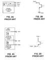
- FIG. 2A depicts an actuator which must be connected to an output module with an output circuit designed for sinking loads.
- FIG. 2B depicts an output circuit which sinks current.
- FIG. 2C depicts a compound actuator made up of two solenoids, such as would be found in a pneumatic valve manifold. Such a compound actuator must be connected to an output module with an output circuit designed for sourcing loads. Note that this compound actuator requires only three conductors to be connected up in order to operate.
- FIG. 2D depicts an output circuit designed to source current to its output terminal.
- the sensors, actuators and input/output circuits depicted in FIGS. 1A-1D and 2 A- 2 D are a small sample of the universe of sensors, actuators and circuits. In a given machine or process, an engineer generally expects all four of these categories of devices to be part of an input/output system. In addition, if analog sensors and actuators are to be used, more categories of input/output circuits will be required.
- FIGS. 3A and 3B depict an actuator 80 with three conductors that are internally connected to the actuator.
- the conductors form what is commonly called a “pig tail”.
- the three conductors 68 grouped together are called a cable 68 B.
- a group of conductors is referred to as a cable.
- the conductors 68 have attached to them connectors 69 B which are for plugging into mating connectors.
- the conductors 68 have no connectors and are suitable for connecting to terminal blocks, a common type of connector.
- FIG. 4A depicts a situation in which mating connectors 69 B and 71 B are used on both ends of the conductor 68 to connect with connectors 69 and 71 on the device 80 and the input/output module 66 , respectively.
- FIG. 4B depicts the situation in which a mating connector is attached to the device end of the conductor 68 whereas the input/output module end is connected with a terminal block connector.
- FIG. 5 is generally representative of the prior art input/output systems in use today in a wide variety of industries around the world. Whether in Programmable Logic Controllers (PLC's) or Distributed Control Systems (DCS), sensors as show in FIGS. 1A-1D are wired to input/output systems using the teaching of FIG. 5 . Because the two sensors shown in FIG. 5 wired to the input/output system are not either both sourcing or both sinking, the prior art requires that two fixed-circuit input modules be used, one a pull-down module for use with the sourcing sensor and the other module a pull-up module for use with the sinking sensor. FIG. 5 shows that the prior art wiring systems require many more wires than needed to simply connect the sensors to the input modules. In this case, ten wires are required to connect six terminals, three on each of the two sensors. In addition, only one input is used on each of the two input modules. In general, the prior art approach results in poor utilization of the channels on the input/output modules.
- PLC's Programm
- Terminal blocks are the preferred wiring system for most PLCs and input/output modules because wire harnesses can become very complex.
- FIG. 6 takes the wiring layout from FIG. 5 and makes it into a wire harness. Note that this harness is very complicated and is essentially a three-dimensional web of conductors. Although harnesses are sometimes used, especially in specialty applications such as airplanes and automobiles, harnesses are inflexible, difficult to design, handle and repair.
- FIG. 7 depicts a system of two output modules connecting the two types of actuators of FIGS. 2A-2D .
- two typical actuator groups have been selected—one requiring a sourcing output and one requiring a sinking output. Therefore, two output modules are required to complete the system.
- the output circuit of FIG. 7 requires ten conductors to connect six terminals of the two types of actuators.
- only three of sixteen output channels on the two output modules of FIG. 7 are used and only two of sixteen input channels on the two input modules of FIG. 5 are used. This is an inefficient use of the I/O channels.
- FIG. 8 the wiring harness for the output circuit of FIG. 7 is shown.
- the harness of FIG. 8 is also complex.
- a major limitation of the prior art is that the harness of FIG. 6 is different from the harness of FIG. 8 .
- a user of input/output systems must use two different harnesses. The fact that harnesses in general are unique and custom helps to explain why those skilled in the art prefer to use individual wires and terminal block connectors because the interconnections can be built piece-by-piece.
- an input/output module includes: a device communication connector apparatus for connecting at least one conductor between the module and at least one device; interface apparatus for causing the module to place any of a plurality of signals on any of a plurality of contacts of the device communication connector apparatus; wherein the interface apparatus includes at least one electronic integrated circuit providing a selectable interconnection apparatus to a particular one of the contacts; and wherein the interface apparatus is configurable by a user of the module.
- the device communication connector apparatus may include one or more of a terminal block for connecting individual wires and a standard mating connector for connecting wires or cables.
- the selectable interconnection apparatus may be an input, output or power supply.
- the selectable interconnection apparatus may be a sourcing, sinking, analog, digital, frequency measurement, frequency generation, serial communication receiver or serial communication transmitting circuit.
- the electronic integrated circuit may be an ASIC or a hybrid integrated circuit.
- the interface apparatus may include one or more of a multi-chip module and/or a system-in-a-package.
- the I/O module of the present invention is configurable, so as to place any of a plurality of signals on any of a plurality of contacts of the device communication connector, by selecting an interconnection apparatus for each of the contacts.
- the interface apparatus includes at least one electronic integrated circuit providing a selectable interconnection apparatus to a particular one of the contacts in response to user input.
- User input may be one or more of: communications to the module over a network, configuration of jumper blocks on a module circuit board, and instructional data stored in a module memory.
- a method for configuring I/O channels on a configurable connectorized system, the system comprising a module including (i) a device communication connector apparatus with a plurality of contacts and (ii) an interface apparatus including at least one electronic integrated circuit providing a selectable interconnection apparatus to a corresponding at least one of the contacts, the method comprising the step of commanding the interface apparatus to place any of a plurality of signals on any of the plurality of contacts of the device communication connector.
- the commanding step may include one or more of: receiving instructions from a controller apparatus, communications to the module over a network, configuration of jumper blocks on a module circuit board, and receiving instructions in the form of data stored in a module memory.
- the system may further include an embedded web server programmed to provide configuration pages for devices connected to the device communication connector.
- a system user may: (a) connect the module to a personal computer; (b) open one of the configuration pages; and (c) provide inputs on the personal computer to determine a specific interconnection apparatus for each of the contacts.
- a method for directing a signal between a system controller and at least one device using a configurable connectorized system, the system comprising a module including (i) a device communication connector apparatus with a plurality of contacts and (ii) an interface apparatus including at least one electronic integrated circuit providing a selectable interconnection apparatus to a corresponding at least one of the contacts, the method comprising the steps of: (a) creating a signal path between the system controller and the module; (b) connecting at least one conductor between the device communication connector apparatus and a first device; and (c) causing the module to place any of a plurality of signals on any of the plurality of contacts of the device communication connector apparatus.
- the method may further comprise the step of connecting at least one conductor between the device communication connector apparatus and a second device.
- FIG. 1A is a schematic of a sensor which sources current at its output terminal.
- FIG. 1B is a schematic of an input circuit intended to be connected to a sourcing sensor.
- FIG. 1C is a schematic of a sensor which sinks current at its output terminal.
- FIG. 1D is a schematic of an input circuit intended to be connected to a sinking sensor.
- FIG. 2A is a schematic of an actuator intended to be connected to an output circuit which sinks current at its output terminal.
- FIG. 2B is a schematic of an output circuit which sinks current at its output terminal.
- FIG. 2C is a schematic of an actuator intended to be connected to an output circuit which sources current at its output terminal.
- FIG. 2D is a schematic of an output circuit which sources current at its output terminal.
- FIG. 3A is a schematic of a pig tail sensor with mating connectors on the end of the pig tail.
- FIG. 3B is a schematic of a pig tail sensor with no mating connectors on the end of the pig tail, and therefore intended to be connected to terminal block connectors.
- FIG. 4A is a schematic of a device connected to an input/output module employing mating connectors on both ends of the conductor.
- FIG. 4B is a schematic of a device connected to an input/output module employing a mating connector at the device-end of the conductor and no mating connector at the input/output module end of the conductor, therefore intended to be connected to a terminal block connector.
- FIG. 5 is a schematic of a prior art system of two input modules connected to two sensors, one sinking and one sourcing.
- FIG. 6 shows the interconnection wiring of the system of FIG. 5 .
- FIG. 7 is a schematic of a prior art system of two output modules connected to two actuators, one intended to connect to a sinking output circuit and one intended to connect to a sourcing output circuit.
- FIG. 8 shows the interconnection wiring of the system of FIG. 7 .
- FIG. 9 is a schematic of a configurable input/output system connected to a sinking sensor, a sourcing sensor, an actuator intended to be connected to a sinking output circuit and an actuator intended to be connected to a sourcing output circuit, according to the invention.
- FIG. 10 shows the interconnection wiring of the system of FIG. 9 .
- FIG. 11 is a schematic of the configurable interface apparatus, according to the invention.
- FIG. 12 is a schematic of an integrated circuit performing the function of the configurable interface apparatus of the invention.
- FIG. 13 is a schematic of a configurable input/output system as in FIG. 9 with the addition of a thermocouple connected in such a manner as to measure the differential voltage across the thermocouple, according to the invention.
- the present invention contemplates a configurable I/O module for use in efficiently connecting sensors and actuators to a controller.
- the configurable I/O module is not limited to this use.
- the module may be used in a system without connecting to a system controller.
- the module may operate in a stand-alone fashion, for example performing temperature control.
- the module may operate as an embedded controller wherein the module acts as a machine controller, for example.
- the module is configurable by the user and various methods are available to the user for configuration of the module.
- FIG. 9 a block diagram shows a configurable connectorized system including an input/output system 65 connecting sensors and actuators 80 - 84 to a system controller 72 .
- Configurable input/output system 65 includes an input/output module 66 , the module being one or more circuit boards optionally mounted in an enclosure or plugged into a backplane.
- the module 66 includes one or more device communication connectors 69 .
- the device communication connectors 69 may be a simple terminal block connector to which a single conductor or a plug-type connector may be connected. The plug may hold one or multiple conductors.
- FIG. 9 shows the most general case in which all of the device communication connectors 69 hold a single conductor.
- the conductors 68 interconnect the devices 80 - 84 to the configurable input/output module 66 .
- the devices may contain device-end connectors 71 which may or may not be similar to the device communication connectors 69 .
- the conductors 68 may optionally have affixed to them connectors 69 B and 71 B which mate with the respective input/output module device communication connectors 69 and device-end connectors 71 , respectively.
- the conductors 68 have no connectors 69 B and/or 71 B and are connected directly to the device communication connectors 69 and/or the device-end connectors 71 . Such direct connection could employ terminal block connectors, for example, as described above.
- the conductors 68 may be grouped into cables.
- All of the cables 68 B are preferably identical, but the present invention also allows for cables 68 B with differing numbers and configuration of conductors.
- the device communication connectors 69 and device-end connectors 71 may similarly be grouped so as to match the number of conductors of the cables. By so doing, an entire cable may be connected/disconnected from either a device or the input/output module or both.
- no device-end connector 71 is employed at all, which results if, for example, any device 80 - 84 is manufactured with a pig tail arrangement where the conductors 68 are already attached to the device.
- the pig tail may be connected directly to device communication connectors 69 , which may be a terminal block.
- the pig tail may have connectors 69 B attached to the ends of the conductors, and the connectors may be connected directly to the device communication connectors 69 .
- the connectors 69 B and 71 B may be attached to the conductors 68 by being crimped, soldered, welded, brazed or similarly affixed.
- the conductors may be directly clamped, for example using screw-driven or spring-type terminal blocks, thus obviating the need for one or both mating connectors 69 B and 71 B.
- the configurable input/output module 66 includes a microprocessor 82 , an internal power supply 91 and an interface apparatus 97 .
- the internal power supply 91 provides power to the interface apparatus 97 , thus enabling power to be supplied from the input/output module 66 to devices 80 - 84 .
- the internal power supply 97 also provides power for the operation of all components of the module 66 .
- the internal power supply 91 is connected to an external power supply 79 .
- the interface apparatus 97 is described in detail below, with reference to FIG. 11 .
- the microprocessor 82 is programmable for effecting a particular directing of a signal between the configurable input/output module 66 and devices 80 - 84 , and between the module 66 and a system controller 72 .
- the microprocessor contains a buffer memory 92 .
- Controller communication connectors 76 provide connection to a network connection 78 (preferably Ethernet) for communication between the module 66 and the system controller 72 .
- the network connection 78 may be a cable with standard connectors 76 B which allow the cable to be readily attached to and detached from the input/output module 66 .
- the network connection 78 may instead be a backplane connector, for example the module 66 may be plugged into a backplane of a PLC or an embedded controller, or the module may function as an embedded controller.
- the network connection 78 may also utilize wireless technology without departing from the essence of the invention.
- the system controller 72 is often used to coordinate multiple configurable input/output modules 66 .
- the configurable I/O module 66 may operate without connection to the system controller 72 .
- a configurable input/output module 66 may: act as a so-called embedded controller; be a circuit board which is a part of a larger system; or function as the system controller by itself.
- FIG. 9 four different sensors and actuators are shown connected to a single configurable input/output module of the present invention.
- a sourcing sensor 80 a sinking sensor 81 , and two actuator types, one designed to be driven by a sourcing output circuit (see 83 & 84 ) and one designed to be driven by a sinking output circuit (see 82 ) are connected to the configurable input/output module 66 .
- an equivalent prior art system will require four different input/output modules.
- FIG. 7 illustrates a prior art system with three actuators and FIG.
- FIG. 5 shows a prior art system with two sensors, from which it can be appreciated that an equivalent prior art system for four different sensors and actuators will require four different input/output modules.
- the present invention accomplishes this requirement with a single, configurable input/output module 66 .
- the prior art systems do not supply power from input/output modules, whereas the present invention employs a configurable I/O connection that supplies power and a ground return.
- the prior art systems poorly utilize the circuits of the four different input and output modules, whereas the present invention utilizes all necessary connections of the configurable input/output module.
- three configurable input/output channels are not required for this set of sensors and actuators. These three channels are therefore available for additional sensors and actuators, should they be needed in the future.
- FIG. 9 demonstrates the superiority of the present invention over the prior art. With the present invention, far fewer connections are required to achieve the same utility as the prior art. In addition, efficient utilization of the input/output module of the present invention is achieved, making distributed control architectures more attractive.
- FIG. 10 shows the wiring layout for the system of FIG. 9 .
- the conductors are shown in four groups corresponding to the four devices.
- the conductors in each group may conveniently be combined into a cable, thus four identical cables can be used.
- FIG. 10 depicts another benefit of the configurable input/output module of the invention.
- the wiring of the prior art was necessarily a complex wire harness that defied attempts at simplification
- the wiring of the present invention is efficient and simple, for example, consisting of separate, simple cables for each of the sensors and actuators.
- the nature of the configurable, connectorized input/output module generally allows standard, identical cable sets to be used because the desired signals can be directed onto the desired contacts.
- FIG. 10 clearly shows how the simplified wire pattern of the present invention encourages cabled, connectorized wiring systems. Being able to use four identical cables greatly simplifies connecting sensors and actuators to the configurable input/output module.
- the present invention facilitates the use of standard cables for connecting to sensors and actuators.
- the use of hand-wired, single-conductor terminal block connectors is not precluded since this configuration is the simplest of standard cable connections.
- Some users of input/output systems prefer hand-wired, single-conductor systems.
- the present invention significantly simplifies such systems and results in much better utilization of the input/output modules.
- FIG. 11 shows input/output module 66 with more detail of the interface apparatus 97 .
- the configurable input/output module 66 may contain any number of interface apparatus 97 A, 97 B, 97 C . . . .
- Each interface apparatus is connected to one device connector 69 and optionally through an internal cross point switch to another interface apparatus. (See FIG. 12 and related description.)
- Each interface apparatus contains any number of interconnection apparatus, each with a relay. In the particular embodiment shown, there are 12 interconnection apparatus and corresponding relays R 1 -R 12 .
- the interface apparatus 97 A is capable of routing any of a plurality of signals and connecting them to the device connector 69 .
- FIG. 11 is highly stylized and is intended to convey the essence of the invention.
- the interface apparatus, shown in FIG. 11 to comprise interconnection apparatus and relays R 1 to R 12 are realized with transistors in preferred embodiments.
- the interface apparatus including interconnection apparatus such as those illustrated in FIG. 11 , may be configured as an integrated circuit (IC).
- the IC is repeated within the I/O module 66 for each device connector 69 .
- the module 66 can contain any number of ICs, just as any module may contain any number of device connectors 69 .
- Another embodiment may employ a different IC architecture in which multiple device connectors 69 are handled in each IC or multiple ICs are used to handle one or more device connectors. The result of using an IC is a dramatic reduction in the size and cost of building a module 66 by virtue of the miniaturization afforded by modern semiconductor processes.
- FIG. 12 is a block diagram of an integrated circuit capable of realizing the interface apparatus, 97 A.
- the integrated circuit 198 has been specifically designed to serve the role of the interconnection apparatus, thus it may be referred to as an Application Specific Integrated Circuit (ASIC).
- ASIC Application Specific Integrated Circuit
- This ASIC is specifically designed to provide the functionality of the interconnection apparatus.
- the term ASIC includes a standard integrated circuit designed to function as the interface apparatus.
- IC integrated circuit
- ASICs application specific integrated circuit
- hybrid ICs low temperature co-fired ceramic (LTCC) hybrid ICs
- MCMs multi-chip modules
- SiP system in a package
- Hybrid ICs are miniaturized electronic circuits that provide the same functionality as a (monolithic) IC.
- MCMs comprise at least two ICs; the interface apparatus of the present invention may be realized by a MCM where the required functionalities are divided between multiple ICs.
- a SiP also known as a Chip Stack MCM is a number of ICs enclosed in a single package or module.
- a SiP can be utilized in the current invention similarly to a MCM.
- programmable logic devices might be used to realize the interface apparatus of the present invention.
- programmable logic devices such as field programmable gate arrays (FPGAs)
- FPGAs field programmable gate arrays
- FIG. 12 depicts a block diagram of a pin driver ASIC 198 .
- the microprocessor 82 of FIG. 11 can command the ASIC 198 to perform the functions of the circuits of interconnection apparatus 97 A.
- the circuitry of FIG. 12 appears different from the interconnection apparatus 97 A, the ASIC 198 is capable of performing the same or similar required functions.
- FIG. 11 is a somewhat idealized diagram intended to convey the essence of the invention, FIG. 12 contains more of the circuit elements that one would place inside an ASIC. Nonetheless, FIG. 12 implements all the circuit elements of FIG. 11 .
- FIG. 11 is a somewhat idealized diagram intended to convey the essence of the invention. 12 contains more of the circuit elements that one would place inside an ASIC. Nonetheless, FIG. 12 implements all the circuit elements of FIG. 11 . For example, FIG.
- FIG. 11 shows a digital-to-analog converter (D/A or DAC) connectable to the device communication connector 69 .
- the digital-to-analog converter 226 is connected to the output pin 208 via the switch 220 .
- the present invention also includes other circuit arrangements for an ASIC 198 for the same or similar purpose. Those skilled in the art will know how to design various such circuitry, and these are to be included in the present invention.
- Power may be applied to pin 208 by closing high current switch 222 b and setting the supply selector 227 to any of the available power supply voltages such as 24-volts, 12-volts, 5-volts, ground or negative 12-volts.
- the ASIC can measure the voltage on pin 208 by closing the low current switch 222 and reading the voltage converted by the analog-to-digital converter 216 .
- thermocouple temperature sensor can be directly connected to ASIC 198 at point/pin 208 , wherein the sensor produces a very low voltage signal.
- a cross-point switch 210 allows a precision differential amplifier 212 to connect to both leads of the thermocouple, one lead of the thermocouple being connected to the node/pin 208 connected to a pin of a connector 69 ( FIG. 11 ), and the second lead of the thermocouple connected to another pin of the connector 69 , which is connected to a 4-way cross-point I/O 214 connector.
- the cross-point switch 210 therefore allows two adjacent pins of a connector 69 to be connected to the same analog-to-digital converter 216 via a differential amplifier 212 .
- ASIC 198 has the ability to measure the amount of current flowing in or out of the node 208 labeled “Pin” in FIG. 12 .
- the pin driver circuit 198 uses its A/D converter 216 to measure current flowing into or out of the pin node 208 , thereby enabling the detection of excessive current, or detecting whether a device connected to the Pin node 208 is functioning or wired correctly.
- ASIC 198 also has the ability to monitor the current flow into and out of the pin node 208 to unilaterally disconnect the circuit 198 , thereby protecting the ASIC 198 from damage from short circuits or other potentially damaging conditions.
- the ASIC 198 employs a so-called “abuse detect circuit” 218 to monitor rapid changes in current that could potentially damage the ASIC 198 .
- Low current switches 220 , 221 and 222 and high current switch 222 b respond to the abuse detect circuit 218 to disconnect the pin 208 .
- the ASIC 198 abuse detect circuit 218 has the ability to establish a current limit for the pin 208 , the current limit being programmatically set by the microprocessor 82 . This is indicated by selections 224 .
- the ASIC 198 can measure the voltage at the pin node 208 in order to allow the microprocessor 82 to determine the state of a digital input connected to the pin node.
- the threshold of a digital input can thereby be programmed rather than being fixed in hardware.
- the threshold of the digital input is set by the microprocessor 82 using the digital-to-analog converter 226 .
- the output of the digital-to-analog converter 226 is applied to one side of a latching comparator 225 .
- the other input to the latching comparator 225 is routed from the pin 208 and represents the digital input. Therefore, when the voltage of the digital input on the pin 208 crosses the threshold set by the digital-to-analog converter, the microprocessor 82 is able to determine the change in the input and thus deduce that the digital input has changed state.
- the ASIC 198 can receive or produce frequency signals. If a serial communication device, for example a printer, is connected to pin 208 , then the frequency signals can be routed through the low current switch 221 and thence to a universal asynchronous receiver transmitter (UART) or similar circuit element (not shown) that can interpret the frequency information. All of the ASICs 198 in a module 66 (see FIG. 11 ) can route the frequency information to one of four wires that make up the frequency bus 230 . By employing the frequency bus 230 , it is possible for the module 66 to receive and transmit frequency signals configured as either single-ended or differential. Such serial electrical standards as RS-422 provide for differential serial information.
- UART universal asynchronous receiver transmitter
- the ASIC 198 can produce a current source at the pin node, the current source being a standard method of connecting various industrial control devices.
- the ASIC 198 can produce signals varying over the standard 4-20 mA and 0-20 mA range.
- This current source means is accomplished by the microprocessor 82 as it causes the digital-to-analog converter 226 to produce a voltage which is routed to a Selectable Gain Voltage Buffer or Current Driver 231 and then through a selectable source resistor 227 , the selectable source resistor 227 being set to the appropriate resistance, by the microprocessor 82 , to achieve the desired output current.
- the current is regulated by the Selectable Gain Voltage Buffer or Current Driver 231 using feedback through the analog switch 229 using path A.
- the ASIC 198 can measure a current signal presented at the pin node, the current signal being produced by various industrial control devices.
- the ASIC 198 can measure signals varying over the standard 4-20 mA and 0-20 mA ranges.
- This current measurement means is accomplished by the microprocessor 82 as it causes the selectable gain voltage buffer 231 to produce a convenient voltage such as zero volts at its output terminal.
- the microprocessor 82 causes the selectable source resistor 228 to present a resistance to the path of current from the industrial control device and its current output. This current enters the ASIC 198 via the pin 208 .
- the imposed voltage on one side of a known resistance will cause the unknown current from the external device to produce a voltage on the pin 208 which is then measured via the analog-to-digital converter 216 through the low current switch 222 .
- the microprocessor 82 uses Ohm's Law to solve for the unknown current being generated by the industrial control device.
- thermocouple or other temperature sensor
- the microprocessor 82 can read the temperature sensor, and activate the heater in such a manner that a desired temperature is achieved.
- the heater usually employs an amplifier (for example a relay) which converts the low-level output of the module 66 into a high-power output capable of driving a heater.
- the module 66 can thereby perform closed loop control.
- the thermocouple would be connected to two adjacent pins 208 configured as inputs, while the heater would be connected to two pins 208 , the heater pins being configured as outputs.
- the microprocessor 82 would measure the voltage of the temperature sensor as described above.
- the microprocessor 82 would apply the desired temperature using known control algorithms to the measured temperature and develop an actuation signal also using the accepted methods.
- the microprocessor would then actuate the heater either with a continuously variable analog signal or via a pulse width modulated (PWM) on/off signal.
- PWM pulse width modulated
- the ASIC 198 includes functions as described above in reference to the interface apparatus 97 .
- an ASIC 198 can include an interconnection apparatus including a digital-to-analog converter 226 , wherein the microprocessor 82 is programmable to direct the reception of a digital signal from the microprocessor 82 and cause the signal to be converted by the digital-to-analog converter 226 to an analog signal, and to place a copy of the analog signal on the pin 208 . See FIGS. 11 and 12 .
- the ASIC 198 can also include an interconnection apparatus including an analog-to-digital converter 216 , and wherein the microprocessor 82 is programmable to detect an analog signal on any selected contact 69 and cause the analog-to-digital converter 216 to convert the signal to a digital signal and output a copy of the digital signal to the microprocessor 82 .
- the ASIC 198 can also include a supply selector 227 , and a high current switch 222 b positioned between the selector 227 and the pin 208 .
- the microprocessor 82 is programmable to operate a supply selector 227 to cause a power supply voltage to be connected to a first contact 69 , and to cause a power supply return to be connected to a second contact 69 .
- a 2 ⁇ 8 cross-point switch 210 that serves to connect a sensor to two adjacent pins 208 which are in turn connected to two adjacent device communication connectors 69 .
- the cross-point switch 210 allows a sensor such as a thermocouple to be connected to a precision differential amplifier 212 .
- the precision differential amplifier 212 may be connected via the low current switch 222 and the 2 ⁇ 8 cross-point switch 210 to the 4-way cross-point I/O 214 and then to another 4-way cross-point I/O 214 on an adjacent integrated circuit 19 (the integrated circuit for an adjacent contact 69 ).
- the microprocessor 82 is generally configured/programmed by a controller 72 to receive instruction from the controller as required to sense a particular selected one of devices 80 - 81 or actuate one of devices 82 - 84 and provide the corresponding data to the system controller.
- the microprocessor 82 is also programmed/directed by the controller 72 to cause a particular signal to be applied to any selected one or more contacts 69 and thereby corresponding conductors 68 .
- the microprocessor 82 is programmed to respond to direction to send a selected signal type from one or more of devices 80 - 84 to the system controller 72 .
- the microprocessor controls the configuration of the interface apparatus 97 and generally the microprocessor is controlled by the system controller.
- the interface apparatus can be configured in response to a message stored in the memory of the microprocessor 82 of the module 66 .
- the interface apparatus can be configured in response to a set of jumper blocks installed on the module circuit board, wherein inserting or removing the jumper blocks determines the configuration.
- the microprocessor 82 has an embedded web server.
- a personal computer may be connected to the system 65 using an Ethernet cable or a wireless communication device and then to the Internet.
- the personal computer may also be a system controller.
- the embedded web server provides configuration pages for each device connected to the module 66 .
- the user then uses a mouse, or other keyboard inputs, to configure the device function and assign input/output pins.
- the user may simply drag and drop icons on the configuration page to determine a specific interconnection apparatus for each of the contacts.
- the microprocessor 82 may be programmed to recognize particular input data, included for example in an Ethernet packet on network cable 78 containing instructions to transmit the data as an analog signal on a particular line 94 to a particular one of devices 80 - 84 .
- the programming in this case would instruct the microprocessor to direct/convert the data through apparatus having a digital to analog converter in interface apparatus 97 . Facility for making this connection is symbolized by relay “R 1 ” which would be activated to make the required connection.
- relay “R 1 ” which would be activated to make the required connection.
- the microprocessor 82 would be programmed to respond to a signal from the controller 72 to activate relay R 6 .
- the system 65 allows communication of a selected variety through any line such as 94 , and application of any one of a variety of signals to be sent to any selected line such as 94 and thence to a corresponding device.
- the circuit switching apparatus (R 1 -R 12 ) are shown diagrammatically as electromechanical relays. In one embodiment, this switching apparatus is realized in a semiconductor circuit. (See FIG. 12 and related description.) A semiconductor circuit can be realized far less expensively and can act faster than an electromechanical relay circuit. An electromechanical relay is used in order to show the essence of the invention.
- FIG. 13 further demonstrates the advantages of configurable adjacent connections of the present invention.
- FIG. 13 shows a thermocouple 101 added to the system of FIG. 9 .
- the embodiment shown in FIG. 9 is more efficient than the prior art in terms of channels used. Three channels remain unused in the system shown in FIG. 9 , specifically device communication connectors numbers 13 , 14 and 15 .
- the thermocouple a type of temperature sensor, is connected to communication connectors 14 and 15 .
- a precision differential amplifier 212 is connected to the thermocouple using the cross-point switch 210 . See FIG. 12 .
- FIG. 13 illustrates the ability of a single configurable input/output module 66 to make connections to sourcing, sinking, digital and analog sensors and actuators simultaneously. Thus making efficient use of the available channels on the I/O module. In contrast, a fixed-configuration prior art input/output module cannot accommodate more than one of these disparate devices. (See FIGS. 5 & 7 .)
Landscapes
- Physics & Mathematics (AREA)
- General Physics & Mathematics (AREA)
- Engineering & Computer Science (AREA)
- Automation & Control Theory (AREA)
- Programmable Controllers (AREA)
Abstract
Description
Claims (20)
Priority Applications (5)
| Application Number | Priority Date | Filing Date | Title |
|---|---|---|---|
| US12/106,968 US7822896B1 (en) | 2001-02-14 | 2008-04-21 | Electronically configurable connector module |
| US13/069,292 US8862452B2 (en) | 2001-02-14 | 2011-03-22 | Control system simulator and simplified interconnection control system |
| US13/281,394 US9013854B2 (en) | 2001-02-14 | 2011-10-25 | Configurable solenoid actuation method and apparatus |
| US14/512,898 US20150248509A1 (en) | 2001-02-14 | 2014-10-13 | Control system simulator and simplified interconnection control system |
| US14/690,795 US20160078990A1 (en) | 2001-02-14 | 2015-04-20 | Configurable Solenoid Actuation Method and Apparatus |
Applications Claiming Priority (7)
| Application Number | Priority Date | Filing Date | Title |
|---|---|---|---|
| US26912901P | 2001-02-14 | 2001-02-14 | |
| US10/071,870 US6892265B2 (en) | 2001-02-14 | 2002-02-08 | Configurable connectorized I/O system |
| US11/043,296 US20050130459A1 (en) | 2001-02-14 | 2005-01-25 | Configurable connectorized I/O system |
| US11/296,134 US7216191B2 (en) | 2001-02-14 | 2005-12-06 | System for programmed control of signal input and output to and from cable conductors |
| US11/801,127 US20070255879A1 (en) | 2001-02-14 | 2007-05-07 | System for programmed control of signal input and output to and from cable conductors |
| US95004007P | 2007-07-16 | 2007-07-16 | |
| US12/106,968 US7822896B1 (en) | 2001-02-14 | 2008-04-21 | Electronically configurable connector module |
Related Parent Applications (3)
| Application Number | Title | Priority Date | Filing Date |
|---|---|---|---|
| US11/801,127 Continuation-In-Part US20070255879A1 (en) | 2001-02-14 | 2007-05-07 | System for programmed control of signal input and output to and from cable conductors |
| US12/106,968 Continuation-In-Part US7822896B1 (en) | 2001-02-14 | 2008-04-21 | Electronically configurable connector module |
| US12/106,968 Continuation US7822896B1 (en) | 2001-02-14 | 2008-04-21 | Electronically configurable connector module |
Related Child Applications (3)
| Application Number | Title | Priority Date | Filing Date |
|---|---|---|---|
| US12/106,968 Continuation-In-Part US7822896B1 (en) | 2001-02-14 | 2008-04-21 | Electronically configurable connector module |
| US12/106,968 Continuation US7822896B1 (en) | 2001-02-14 | 2008-04-21 | Electronically configurable connector module |
| US91144510A Continuation | 2001-02-14 | 2010-10-25 |
Publications (1)
| Publication Number | Publication Date |
|---|---|
| US7822896B1 true US7822896B1 (en) | 2010-10-26 |
Family
ID=42987642
Family Applications (1)
| Application Number | Title | Priority Date | Filing Date |
|---|---|---|---|
| US12/106,968 Expired - Fee Related US7822896B1 (en) | 2001-02-14 | 2008-04-21 | Electronically configurable connector module |
Country Status (1)
| Country | Link |
|---|---|
| US (1) | US7822896B1 (en) |
Cited By (16)
| Publication number | Priority date | Publication date | Assignee | Title |
|---|---|---|---|---|
| US20110106996A1 (en) * | 2007-04-26 | 2011-05-05 | Roberto Rosso | Communications control bus and apparatus for controlling multiple electronic hardware devices |
| US20110231176A1 (en) * | 2001-02-14 | 2011-09-22 | Xio, Inc | Control system simulator and simplified interconnection control system |
| WO2013087302A1 (en) * | 2011-12-14 | 2013-06-20 | Phoenix Contact Gmbh & Co. Kg | Multifunctional input/output module |
| WO2013166050A2 (en) | 2012-04-30 | 2013-11-07 | Xio, Inc. | Configurable, connectorized server-augmented control system |
| US9013854B2 (en) | 2001-02-14 | 2015-04-21 | Xio, Inc. | Configurable solenoid actuation method and apparatus |
| WO2015174971A1 (en) * | 2014-05-14 | 2015-11-19 | Ge Intelligent Platforms, Inc. | Configurable input/output module and method therefore |
| WO2015187687A1 (en) * | 2014-06-02 | 2015-12-10 | Phoenix Contact Development and Manufacturing, Inc. | Universal i/o signal interposer system |
| US20160123624A1 (en) * | 2014-09-30 | 2016-05-05 | Honeywell International Inc. | Universal cell |
| US20170147367A1 (en) * | 2015-11-20 | 2017-05-25 | General Electric Company | Configurable io-channel system with embedded microcontroller |
| GB2567926A (en) * | 2017-09-13 | 2019-05-01 | Fisher Rosemount Systems Inc | System and methods for enhanced modular controller port to port communication |
| US10303149B2 (en) | 2015-01-28 | 2019-05-28 | Mitsubishi Electric Corporation | Intelligent function unit and programmable logic controller system |
| US10551815B2 (en) | 2017-09-13 | 2020-02-04 | Fisher-Rosemount Systems, Inc. | Systems and methods for enhanced modular controller port to port communication |
| WO2021137904A1 (en) * | 2020-01-03 | 2021-07-08 | Phoenix Contact Development and Manufacturing, Inc. | Convertible i/o signal processor for a process control network |
| CN113138583A (en) * | 2020-01-20 | 2021-07-20 | 耐莱斯美国股份有限公司 | Self-learning device for connecting a programmable logic controller to a field device |
| CN115021744A (en) * | 2022-08-09 | 2022-09-06 | 南方电网数字电网研究院有限公司 | Programmable wiring nano relay array, and optimized wiring method and system |
| WO2025221421A1 (en) * | 2024-04-19 | 2025-10-23 | Siemens Aktiengesellschaft | Module with selectable digital outputs |
Citations (28)
| Publication number | Priority date | Publication date | Assignee | Title |
|---|---|---|---|---|
| US3795901A (en) | 1972-12-29 | 1974-03-05 | Ibm | Data processing memory system with bidirectional data bus |
| US4360913A (en) | 1980-03-17 | 1982-11-23 | Allen-Bradley Company | Multiplexing I/O module |
| US4695955A (en) | 1983-12-26 | 1987-09-22 | A2F | Electronic device providing a universal interface between sensors and an acquisition and processing unit of the signals originating from said sensors |
| US4954949A (en) | 1988-02-05 | 1990-09-04 | Commodore-Amiga, Inc. | Universal connector device for bus networks in host computer/co-processor computer system |
| EP0436458A2 (en) | 1990-01-04 | 1991-07-10 | International Business Machines Corporation | Programmable connector |
| US5064387A (en) | 1990-06-12 | 1991-11-12 | Thomas & Betts Corporation | Shielded electrical jack connector |
| US5327098A (en) | 1993-07-29 | 1994-07-05 | Burr-Brown Corporation | Programmable gain amplifier circuitry and method for biasing JFET gain switches thereof |
| US5371858A (en) * | 1989-01-31 | 1994-12-06 | Norand Corp. | Data communication system for assigning addresses to hand-held data terminals |
| US5379184A (en) | 1991-08-30 | 1995-01-03 | Unisys Corporation | Pry-in/pry-out disk drive receptacle |
| US5423697A (en) | 1994-05-26 | 1995-06-13 | Intel Corporation | Modular communications connector for I/O card applications |
| US5596169A (en) | 1995-05-12 | 1997-01-21 | Iomega Corporation | Combined SCSI/parallel port cable |
| US5630170A (en) | 1994-10-12 | 1997-05-13 | Kabushiki Kaisha Sega Enterprises | System and method for determining peripheral's communication mode over row of pins disposed in a socket connector |
| US5635841A (en) | 1995-03-31 | 1997-06-03 | Innova Electronic Corporation | Electronic ignition control module test system |
| US5659800A (en) * | 1993-10-06 | 1997-08-19 | International Technologies & Systems Corporation (Its) | System for directly sending undecoded raw signals from reader device via external slave interface to personal computer through communication port without first decoding the signals |
| US5696988A (en) | 1995-10-04 | 1997-12-09 | Ge Fanuc Automation North America, Inc. | Current/voltage configurable I/O module having two D/A converters serially coupled together such that data stream flows through the first D/A to the second D/A |
| US5701515A (en) | 1994-06-16 | 1997-12-23 | Apple Computer, Inc. | Interface for switching plurality of pin contacts to transmit data line and plurality of pin contacts to receive data line to interface with serial controller |
| US5872999A (en) | 1994-10-12 | 1999-02-16 | Sega Enterprises, Ltd. | System for peripheral identification obtained by calculation and manipulation data collecting for determining communication mode and collecting data from first terminal contacts |
| US5897399A (en) | 1997-01-16 | 1999-04-27 | Hewlett-Packard Company | Versatile input/output control and power distribution block for use with automated tooling |
| US5905249A (en) * | 1991-11-04 | 1999-05-18 | Spectra-Physics Scanning Systems, Inc. | Multiple-interface selection system for computer peripherals |
| US5938754A (en) * | 1997-11-26 | 1999-08-17 | National Instruments Corporation | Fieldbus connector including dual connectors |
| US5983290A (en) * | 1993-11-09 | 1999-11-09 | Fujitsu Limited | Information processing system using portable terminal unit and data communication adapter therefor |
| US6301633B1 (en) | 1997-12-31 | 2001-10-09 | Cisco Technology, Inc. | Generic serial interface with automatic reconfigurability |
| US6349235B1 (en) | 1998-11-17 | 2002-02-19 | Rockwell Automation Technologies, Inc. | Programmable logic controller system and method for module number assignment |
| US6375344B1 (en) * | 1989-01-31 | 2002-04-23 | George E. Hanson | Data capture system with communicating and recharging docking apparatus and hand-held data terminal means cooperable therewith |
| US6553432B1 (en) | 1999-10-26 | 2003-04-22 | Dell Usa, L.P. | Method and system for selecting IDE devices |
| US6651877B2 (en) | 1999-12-22 | 2003-11-25 | Kabushiki Kaisha Nippon Conlux | Multi-ROM writer and control method thereof |
| US6892265B2 (en) | 2001-02-14 | 2005-05-10 | Berkley Process Control, Inc. | Configurable connectorized I/O system |
| US7003608B2 (en) | 2003-06-12 | 2006-02-21 | International Business Machines Corporation | Method and system for automatic configuration of IDE bus devices |
-
2008
- 2008-04-21 US US12/106,968 patent/US7822896B1/en not_active Expired - Fee Related
Patent Citations (29)
| Publication number | Priority date | Publication date | Assignee | Title |
|---|---|---|---|---|
| US3795901A (en) | 1972-12-29 | 1974-03-05 | Ibm | Data processing memory system with bidirectional data bus |
| US4360913A (en) | 1980-03-17 | 1982-11-23 | Allen-Bradley Company | Multiplexing I/O module |
| US4695955A (en) | 1983-12-26 | 1987-09-22 | A2F | Electronic device providing a universal interface between sensors and an acquisition and processing unit of the signals originating from said sensors |
| US4954949A (en) | 1988-02-05 | 1990-09-04 | Commodore-Amiga, Inc. | Universal connector device for bus networks in host computer/co-processor computer system |
| US6375344B1 (en) * | 1989-01-31 | 2002-04-23 | George E. Hanson | Data capture system with communicating and recharging docking apparatus and hand-held data terminal means cooperable therewith |
| US5371858A (en) * | 1989-01-31 | 1994-12-06 | Norand Corp. | Data communication system for assigning addresses to hand-held data terminals |
| EP0436458A2 (en) | 1990-01-04 | 1991-07-10 | International Business Machines Corporation | Programmable connector |
| US5064387A (en) | 1990-06-12 | 1991-11-12 | Thomas & Betts Corporation | Shielded electrical jack connector |
| US5379184A (en) | 1991-08-30 | 1995-01-03 | Unisys Corporation | Pry-in/pry-out disk drive receptacle |
| US5905249A (en) * | 1991-11-04 | 1999-05-18 | Spectra-Physics Scanning Systems, Inc. | Multiple-interface selection system for computer peripherals |
| US5327098A (en) | 1993-07-29 | 1994-07-05 | Burr-Brown Corporation | Programmable gain amplifier circuitry and method for biasing JFET gain switches thereof |
| US5659800A (en) * | 1993-10-06 | 1997-08-19 | International Technologies & Systems Corporation (Its) | System for directly sending undecoded raw signals from reader device via external slave interface to personal computer through communication port without first decoding the signals |
| US5983290A (en) * | 1993-11-09 | 1999-11-09 | Fujitsu Limited | Information processing system using portable terminal unit and data communication adapter therefor |
| US5423697A (en) | 1994-05-26 | 1995-06-13 | Intel Corporation | Modular communications connector for I/O card applications |
| US5701515A (en) | 1994-06-16 | 1997-12-23 | Apple Computer, Inc. | Interface for switching plurality of pin contacts to transmit data line and plurality of pin contacts to receive data line to interface with serial controller |
| US5630170A (en) | 1994-10-12 | 1997-05-13 | Kabushiki Kaisha Sega Enterprises | System and method for determining peripheral's communication mode over row of pins disposed in a socket connector |
| US5872999A (en) | 1994-10-12 | 1999-02-16 | Sega Enterprises, Ltd. | System for peripheral identification obtained by calculation and manipulation data collecting for determining communication mode and collecting data from first terminal contacts |
| US5635841A (en) | 1995-03-31 | 1997-06-03 | Innova Electronic Corporation | Electronic ignition control module test system |
| US5596169A (en) | 1995-05-12 | 1997-01-21 | Iomega Corporation | Combined SCSI/parallel port cable |
| US5696988A (en) | 1995-10-04 | 1997-12-09 | Ge Fanuc Automation North America, Inc. | Current/voltage configurable I/O module having two D/A converters serially coupled together such that data stream flows through the first D/A to the second D/A |
| US6077125A (en) | 1997-01-16 | 2000-06-20 | Hewlett-Packard Company | Versatile input/output control and power distribution block for use with automated tooling |
| US5897399A (en) | 1997-01-16 | 1999-04-27 | Hewlett-Packard Company | Versatile input/output control and power distribution block for use with automated tooling |
| US5938754A (en) * | 1997-11-26 | 1999-08-17 | National Instruments Corporation | Fieldbus connector including dual connectors |
| US6301633B1 (en) | 1997-12-31 | 2001-10-09 | Cisco Technology, Inc. | Generic serial interface with automatic reconfigurability |
| US6349235B1 (en) | 1998-11-17 | 2002-02-19 | Rockwell Automation Technologies, Inc. | Programmable logic controller system and method for module number assignment |
| US6553432B1 (en) | 1999-10-26 | 2003-04-22 | Dell Usa, L.P. | Method and system for selecting IDE devices |
| US6651877B2 (en) | 1999-12-22 | 2003-11-25 | Kabushiki Kaisha Nippon Conlux | Multi-ROM writer and control method thereof |
| US6892265B2 (en) | 2001-02-14 | 2005-05-10 | Berkley Process Control, Inc. | Configurable connectorized I/O system |
| US7003608B2 (en) | 2003-06-12 | 2006-02-21 | International Business Machines Corporation | Method and system for automatic configuration of IDE bus devices |
Non-Patent Citations (5)
| Title |
|---|
| "The effects of the Main Variables in the Percussive Arc Welding of Electrical Interconnections," by Holley et al. (abstract only) Publication date: Dec. 1965. |
| Beaman, B., "High Performance Mainframe Computer Cables" (abstract only). |
| Marshall, RC, "A New Approach to Couple/Decouple Networks fro EMC Testing" (Jul. 12-13, 1999) (abstract only). |
| Mikjc-Rakjc, M. et al., "A Connector-Aware Middleware for Distributed Deployment and Mobility," (May 19-22, 2003) (abstract only). |
| Sasaki, S., et al., "High-density and high-pin count flexible SMD Connector for High-Speed Data Bus" (abstract only). |
Cited By (33)
| Publication number | Priority date | Publication date | Assignee | Title |
|---|---|---|---|---|
| US20110231176A1 (en) * | 2001-02-14 | 2011-09-22 | Xio, Inc | Control system simulator and simplified interconnection control system |
| US8862452B2 (en) | 2001-02-14 | 2014-10-14 | Xio, Inc. | Control system simulator and simplified interconnection control system |
| US9013854B2 (en) | 2001-02-14 | 2015-04-21 | Xio, Inc. | Configurable solenoid actuation method and apparatus |
| US20110106996A1 (en) * | 2007-04-26 | 2011-05-05 | Roberto Rosso | Communications control bus and apparatus for controlling multiple electronic hardware devices |
| US8583843B2 (en) * | 2007-04-26 | 2013-11-12 | Roberto Rosso | Communications control bus and apparatus for controlling multiple electronic hardware devices |
| WO2013087302A1 (en) * | 2011-12-14 | 2013-06-20 | Phoenix Contact Gmbh & Co. Kg | Multifunctional input/output module |
| WO2013166050A2 (en) | 2012-04-30 | 2013-11-07 | Xio, Inc. | Configurable, connectorized server-augmented control system |
| US10404529B2 (en) | 2012-04-30 | 2019-09-03 | Xio, Inc. | Configurable, connectorized server-augmented control system |
| WO2015174971A1 (en) * | 2014-05-14 | 2015-11-19 | Ge Intelligent Platforms, Inc. | Configurable input/output module and method therefore |
| WO2015187687A1 (en) * | 2014-06-02 | 2015-12-10 | Phoenix Contact Development and Manufacturing, Inc. | Universal i/o signal interposer system |
| CN106462131A (en) * | 2014-06-02 | 2017-02-22 | 凤凰通讯发展及制造股份有限公司 | Universal I/O signal interposer system |
| JP2017517075A (en) * | 2014-06-02 | 2017-06-22 | フェニックス コンタクト ディベロップメント アンド マニュファクチャリング、インコーポレイテッド | Universal I/O Signal Interposer System |
| US9971727B2 (en) | 2014-06-02 | 2018-05-15 | Phoenix Contact Development and Manufacturing, Inc. | Universal I/O signal interposer system |
| CN106462131B (en) * | 2014-06-02 | 2019-01-25 | 凤凰通讯发展及制造股份有限公司 | Universal I/O Signal Inserter System |
| US20160123624A1 (en) * | 2014-09-30 | 2016-05-05 | Honeywell International Inc. | Universal cell |
| US10678204B2 (en) * | 2014-09-30 | 2020-06-09 | Honeywell International Inc. | Universal analog cell for connecting the inputs and outputs of devices |
| US10303149B2 (en) | 2015-01-28 | 2019-05-28 | Mitsubishi Electric Corporation | Intelligent function unit and programmable logic controller system |
| US20170147367A1 (en) * | 2015-11-20 | 2017-05-25 | General Electric Company | Configurable io-channel system with embedded microcontroller |
| US9940285B2 (en) * | 2015-11-20 | 2018-04-10 | General Electric Company | Configurable IO-channel system with embedded microcontroller |
| GB2567926A (en) * | 2017-09-13 | 2019-05-01 | Fisher Rosemount Systems Inc | System and methods for enhanced modular controller port to port communication |
| US10551815B2 (en) | 2017-09-13 | 2020-02-04 | Fisher-Rosemount Systems, Inc. | Systems and methods for enhanced modular controller port to port communication |
| GB2567926B (en) * | 2017-09-13 | 2022-10-26 | Fisher Rosemount Systems Inc | System and methods for enhanced modular controller port to port communication |
| CN114902147A (en) * | 2020-01-03 | 2022-08-12 | 菲尼克斯电气开发及制造股份有限公司 | Convertible I/O signal processor for process control network |
| WO2021137904A1 (en) * | 2020-01-03 | 2021-07-08 | Phoenix Contact Development and Manufacturing, Inc. | Convertible i/o signal processor for a process control network |
| CN114902147B (en) * | 2020-01-03 | 2025-10-31 | 菲尼克斯电气开发及制造股份有限公司 | Convertible I/O signal processor for process control network |
| US11093428B2 (en) | 2020-01-03 | 2021-08-17 | Phoenix Contact Development and Manufacturing, Inc. | Convertible I/O signal processor for a process control network |
| EP3851926A1 (en) * | 2020-01-20 | 2021-07-21 | Neles USA Inc. | Self-learning apparatus for connecting inputs and outputs of a programmable logic controller to a field device |
| US11138137B2 (en) | 2020-01-20 | 2021-10-05 | Neles Usa Inc. | Self-learning apparatus for connecting inputs and outputs of a programmable logic controller to a field device |
| CN113138583A (en) * | 2020-01-20 | 2021-07-20 | 耐莱斯美国股份有限公司 | Self-learning device for connecting a programmable logic controller to a field device |
| CN115021744A (en) * | 2022-08-09 | 2022-09-06 | 南方电网数字电网研究院有限公司 | Programmable wiring nano relay array, and optimized wiring method and system |
| CN115021744B (en) * | 2022-08-09 | 2022-12-27 | 南方电网数字电网研究院有限公司 | Programmable wiring nano relay array, and optimized wiring method and system |
| WO2025221421A1 (en) * | 2024-04-19 | 2025-10-23 | Siemens Aktiengesellschaft | Module with selectable digital outputs |
| US12542554B2 (en) | 2024-04-19 | 2026-02-03 | Siemens Aktiengesellschaft | Module with selectable digital outputs |
Similar Documents
| Publication | Publication Date | Title |
|---|---|---|
| US7822896B1 (en) | Electronically configurable connector module | |
| US7216191B2 (en) | System for programmed control of signal input and output to and from cable conductors | |
| US10989726B2 (en) | Laboratory sample distribution system and method of operating a laboratory sample distribution system | |
| US8339804B2 (en) | Programmable routing module | |
| US20020119706A1 (en) | Configurable connectorized I/O system | |
| EP4042247B1 (en) | Input/output apparatus and methods for monitoring and/or controlling dynamic environments | |
| US20110231176A1 (en) | Control system simulator and simplified interconnection control system | |
| CN110119369A (en) | Flexible expansible automation equipment with hot-swappable I/O unit | |
| CA3158770C (en) | Input/output apparatus and methods for monitoring and/or controlling dynamic environments | |
| JP7568830B2 (en) | I/O unit and communication system | |
| CN117063135A (en) | I/O unit, main unit and communication system | |
| CN104204970A (en) | Connection modules for field devices in Ex areas | |
| JP2000174673A (en) | Signal conversion unit |
Legal Events
| Date | Code | Title | Description |
|---|---|---|---|
| AS | Assignment |
Owner name: BERKELEY PROCESS CONTROL, INC., CALIFORNIA Free format text: ASSIGNMENT OF ASSIGNORS INTEREST;ASSIGNORS:SAGUES, PAUL;BRASFIELD, LARRY;MOY, PETER K.;REEL/FRAME:021510/0969 Effective date: 20080828 |
|
| STCF | Information on status: patent grant |
Free format text: PATENTED CASE |
|
| AS | Assignment |
Owner name: XIO, INC., CALIFORNIA Free format text: ASSIGNMENT OF ASSIGNORS INTEREST;ASSIGNOR:BERKELEY PROCESS CONTROL, INC.;REEL/FRAME:025923/0461 Effective date: 20090113 |
|
| FPAY | Fee payment |
Year of fee payment: 4 |
|
| MAFP | Maintenance fee payment |
Free format text: PAYMENT OF MAINTENANCE FEE, 8TH YR, SMALL ENTITY (ORIGINAL EVENT CODE: M2552) Year of fee payment: 8 |
|
| FEPP | Fee payment procedure |
Free format text: MAINTENANCE FEE REMINDER MAILED (ORIGINAL EVENT CODE: REM.); ENTITY STATUS OF PATENT OWNER: SMALL ENTITY |
|
| LAPS | Lapse for failure to pay maintenance fees |
Free format text: PATENT EXPIRED FOR FAILURE TO PAY MAINTENANCE FEES (ORIGINAL EVENT CODE: EXP.); ENTITY STATUS OF PATENT OWNER: SMALL ENTITY |
|
| STCH | Information on status: patent discontinuation |
Free format text: PATENT EXPIRED DUE TO NONPAYMENT OF MAINTENANCE FEES UNDER 37 CFR 1.362 |
|
| FP | Lapsed due to failure to pay maintenance fee |
Effective date: 20221026 |