US7813068B2 - Degauss control for magnetic disk-drive preamplifier - Google Patents
Degauss control for magnetic disk-drive preamplifier Download PDFInfo
- Publication number
- US7813068B2 US7813068B2 US12/120,525 US12052508A US7813068B2 US 7813068 B2 US7813068 B2 US 7813068B2 US 12052508 A US12052508 A US 12052508A US 7813068 B2 US7813068 B2 US 7813068B2
- Authority
- US
- United States
- Prior art keywords
- current
- magnitude
- reference current
- degauss
- transistor
- Prior art date
- Legal status (The legal status is an assumption and is not a legal conclusion. Google has not performed a legal analysis and makes no representation as to the accuracy of the status listed.)
- Active, expires
Links
Images


Classifications
-
- G—PHYSICS
- G11—INFORMATION STORAGE
- G11B—INFORMATION STORAGE BASED ON RELATIVE MOVEMENT BETWEEN RECORD CARRIER AND TRANSDUCER
- G11B5/00—Recording by magnetisation or demagnetisation of a record carrier; Reproducing by magnetic means; Record carriers therefor
- G11B5/465—Arrangements for demagnetisation of heads
-
- G—PHYSICS
- G11—INFORMATION STORAGE
- G11B—INFORMATION STORAGE BASED ON RELATIVE MOVEMENT BETWEEN RECORD CARRIER AND TRANSDUCER
- G11B5/00—Recording by magnetisation or demagnetisation of a record carrier; Reproducing by magnetic means; Record carriers therefor
- G11B2005/0002—Special dispositions or recording techniques
- G11B2005/0005—Arrangements, methods or circuits
- G11B2005/001—Controlling recording characteristics of record carriers or transducing characteristics of transducers by means not being part of their structure
- G11B2005/0013—Controlling recording characteristics of record carriers or transducing characteristics of transducers by means not being part of their structure of transducers, e.g. linearisation, equalisation
- G11B2005/0016—Controlling recording characteristics of record carriers or transducing characteristics of transducers by means not being part of their structure of transducers, e.g. linearisation, equalisation of magnetoresistive transducers
- G11B2005/0018—Controlling recording characteristics of record carriers or transducing characteristics of transducers by means not being part of their structure of transducers, e.g. linearisation, equalisation of magnetoresistive transducers by current biasing control or regulation
Definitions
- This invention relates to electronic circuits, and more specifically to degauss control for a magnetic disk-drive preamplifier.
- Driver circuits and preamplifier circuits are used in numerous applications, such as for writing data to a magnetic medium. Due to the increasing demand for faster data transfer, some driver and preamplifier circuits may be required to support a very rapid data-rate. To support such an increase in data-rate for magnetic disk-drives, the recording density of the data-carrying magnetic dipoles on the magnetic disk can be increased. As a result, a greater amount of data can be read from and written to the magnetic disk at a given speed of rotation of the spindle motor of the magnetic disk-drive.
- One embodiment of the invention includes a preamplifier system for a magnetic disk-drive.
- the system includes a current distributor configured to generate a reference current and to decay the reference current from a first magnitude to a second magnitude during a degauss period to degauss a magnetic disk write head.
- the degauss period defines a transition from a write cycle to a read cycle of the magnetic disk-drive and has a predetermined time duration that is independent of the first magnitude of the reference current during the write cycle.
- An output driver is configured to provide a write current to the magnetic disk write head having a magnitude with an absolute value that is based on the reference current.
- the write current can be provided with a polarity to correspond to data being written to an associated magnetic disk during the write cycle.
- Another embodiment of the invention includes a method for degaussing a magnetic disk write head in a magnetic disk-drive.
- the method comprises initiating a degauss period in response to a degauss control signal in response to concluding a write cycle associated with the magnetic disk-drive.
- the method also comprises decoupling a current-mirror that comprises a first mirror transistor that is configured to conduct a magnitude control current and a second mirror transistor configured to conduct a reference current that is provided to cause data to be written to the magnetic disk write head via at least one output driver.
- the method also comprises generating a decay current that flows from a bias terminal of the second mirror transistor.
- the decay current can have a magnitude that is proportional to a square-root of an initial magnitude of the reference current.
- the method further comprises decaying the reference current from the initial magnitude to a predetermined threshold magnitude during the degauss period in response to the decay current.
- Another embodiment of the invention includes a current distribution system for a magnetic disk-drive.
- the system includes means for generating at least one reference current based on an input control signal.
- the system also includes means for driving at least one write current to a respective at least one magnetic disk write head during a write cycle, the at least one write current having a magnitude depending on the at least one reference current.
- the system also includes means for decaying the at least one reference current during a degauss period from a first magnitude to a second magnitude so that the write current decreases proportionally.
- the degauss period defines a transition from the write cycle to a read cycle of the magnetic disk-drive and having a predetermined time duration that is independent of the first magnitude of the reference current during the write cycle.
- FIG. 1 illustrates an example of a preamplifier system in accordance with an aspect of the invention.
- FIG. 2 illustrates an example of timing diagrams associated with a preamplifier system in accordance with an aspect of the invention.
- FIG. 3 illustrates an example of a reference current generator in accordance with an aspect of the invention
- FIG. 4 illustrates an example of a degauss circuit in accordance with an aspect of the invention.
- FIG. 5 illustrates an example of a timing diagram in accordance with an aspect of the invention.
- FIG. 6 illustrates another example of a preamplifier system in accordance with an aspect of the invention.
- FIG. 7 illustrates an example of a method for degaussing a magnetic disk write head in accordance with an aspect of the invention.
- a preamplifier circuit for a magnetic disk drive includes a reference current distributor that can receive a control signal that sets an absolute magnitude of a write current corresponding to data to be written to the magnetic disk, and can generate a reference current based on the control signal that is provided to the magnetic disk write head as a write current via an output driver.
- the control signal can be a control current that can be mirrored as the reference current.
- a current is generated that is proportional to the control current, and thus proportional to an initial magnitude of the reference current.
- the proportional current can be mirrored from the control current, and can thus be substantially equal to the initial magnitude of the reference current.
- the proportional current is provided to a degauss circuit in the reference current distributor.
- the degauss circuit is configured to generate a decay current based on the proportional current, such that the decay current is functionally related to the initial magnitude reference current.
- the decay current can be approximately equal to a square-root of a product of the proportional current and a constant.
- the constant can correspond to a predetermined substantially fixed current that is generated in the degauss circuit and can have a magnitude that is set to define the time duration of the degauss period.
- the decay current flows to or from the gate of a transistor through which the reference current flows, depending on whether the transistor is N-type or P-type. Therefore, the transistor is gradually deactivated by the flow of the decay current, such as by discharging a gate capacitor, at a rate that is based on the magnitude of the reference current. As a result, the reference current, and thus the write current, is likewise decayed at a rate that is based on the initial magnitude of the reference current. Because the decay current has a magnitude that is functionally related to the initial magnitude of the reference current, the degauss period has a time duration that is independent of the initial magnitude of the reference current.
- the time for a degauss period can be accurately controlled (e.g., based on the constant current) regardless of the amount of write current that is provided to the magnetic disk write head.
- a threshold magnitude can be set for the reference current, such that the reference current can be deactivated substantially completely upon the magnitude of the reference current decreasing to the threshold magnitude. Accordingly, the magnetic field that is induced in the magnetic disk write head can be substantially discharged prior to deactivating the reference current to initiate a read operation.
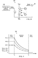
- FIG. 1 illustrates an example of a preamplifier system 10 in accordance with an aspect of the invention.
- the preamplifier system 10 can be implemented in a magnetic disk-drive system, such that the preamplifier system 10 can be implemented to write data onto a magnetic disk (not shown) via a magnetic disk write head 12 .
- the preamplifier system 10 can be implemented in a hard-drive system or in a peripheral disk-drive system.
- the preamplifier system 10 can be implemented in a high recording density disk-drive that is configured to implement perpendicular recording, such that the magnetic dipoles are perpendicular with respect to the plane of the magnetic disk.
- the preamplifier system 10 includes a current controller 14 .
- the current controller 14 can include a digital-to-analog converter (DAC) that converts a digital current magnitude control signal into an analog form.
- DAC digital-to-analog converter
- the current controller 14 provides an analog control current I DAC that is indicative of a magnitude setting for a write current I W that writes data to the magnetic disk.
- the current controller 14 can set a magnitude of the control current I DAC to optimize the magnetic disk write head 12 to a given environment, and can thus vary based on temperature and/or write head characteristics. For a given write cycle, the control current I DAC can therefore be substantially constant.
- the control current I DAC is provided to a reference current distributor 16 .
- the reference current distributor 16 can be configured to generate a reference current I REF based on the control current I DAC .
- the reference current I REF can be generated to be substantially proportional to the control current I DAC during a write cycle.
- the reference current I REF can be generated via a current-mirror from the control current I DAC
- the reference current I REF is provided to an output driver 18 that drives the reference current I REF as a write current I W based on a digital data signal DATA. Therefore, the reference current I REF provides an absolute value magnitude of the write current I W , which is modulated by the digital data signal DATA.
- the write current I W is provided to a bi-directional inductive load in the magnetic disk write head 12 , such that a magnetic field generated by the inductive load can set magnetic dipole elements on the magnetic disk corresponding to the data being written.
- the write current I W can have a magnitude that is substantially centered at zero amps, such that positive values of the write current I W correspond to one binary state of the data to be written to the magnetic disk and negative values of the write current I W correspond to the other binary state of the data to be written to the magnetic disk.
- the write current I W can also include overshoot at transitions from one binary state to the other, such that the magnetic field generated by the inductive load at the magnetic disk write head 12 can be substantially rapidly reversed.
- the preamplifier system 10 can be implemented in a high recording density disk-drive, such as configured to implement perpendicular recording.
- the reference current distributor 16 is configured to decay the reference current I REF to degauss (i.e., demagnetize) the write head 12 during a degauss period that defines a transition between the write cycle and the read cycle.
- a time duration of the degauss period can be set substantially independent of the initial magnitude of the reference current I REF , and thus the write current I W , to provide for accurate and timely degaussing of the write head 12 .
- the reference current distributor 16 includes a degauss circuit 20 .
- a signal DEG_ON is provided to the reference current distributor 16 to initiate a degauss period, and thus to activate the degauss circuit 20 .
- the signal DEG_ON can be provided to one or more switches in the reference current distributor 16 to decouple the reference current I REF from the control current I DAC , such as by decoupling the associated current-mirror, and/or to couple the degauss circuit 20 to the associated transistor through which the current I REF flows.
- the degauss circuit 20 Upon initiation of the degauss period, the degauss circuit 20 is thus configured to decay the reference current I REF from an initial magnitude to a predetermined final value.
- the time duration of the degauss period can be set substantially independent of the initial magnitude of the reference current I REF , and thus also independent of the absolute value magnitude of the write current I W during the preceding write cycle.
- the rate of decay of the reference current I REF can be based on the initial magnitude of the reference current I REF .
- the degauss circuit 20 can be configured to generate a decay current that flows to or from a gate of the transistor through which the reference current I REF flows (i.e., depending on whether the transistor is N-type or P-type).
- the decay current can have a magnitude that is functionally related to the initial magnitude of the reference current I REF during the degauss period.
- the biasing of the transistor is decreased (i.e., gradually deactivated) at a rate that is dependent on the initial magnitude of the reference current I REF , thus setting a time duration of the degauss period that is independent of the initial magnitude of the reference current I REF Accordingly, regardless of the magnitude of the reference current I REF , and thus the write current I W , the degauss period has a consistent time duration. Therefore, variations in the magnitude of the write current I W (e.g., between approximately 10 to 60 mA) are irrelevant to a determination of a time necessary to degauss the magnetic disk write head 12 , such that the magnetic disk write head 12 can be degaussed rapidly and accurately in switching from a write cycle to a read cycle.
- the reference current distributor 16 includes a cutoff circuit 22 that is configured to monitor the reference current I REF .
- the example of FIG. 1 demonstrates the reference current I REF being provided to the cutoff circuit 22 .
- the reference current I REF can be mirrored to the cutoff circuit 22 .
- a signal THRESH can be provided to the cutoff circuit 22 that is indicative of a threshold magnitude associated with the predetermined final value of the reference current I REF .
- the threshold magnitude can be a ratio or percent of the magnitude of the reference current I REF (e.g., 5-20%).
- the cutoff circuit 22 can include a comparator, such that the magnitude of the reference current I REF can be compared with the threshold magnitude that is set by the signal THRESH.
- the cutoff circuit 22 deactivates the reference current I REF , thus concluding the degauss period and initiating the read cycle. Accordingly, the signal THRESH can define a magnitude of the reference current I REF at which the magnetic field of the write head 12 is substantially sufficiently discharged.
- the preamplifier system 10 is not intended to be limited to the example of FIG. 1 .
- the reference current distributor 16 can be configured to selectively distribute the reference current I REF to a plurality of separate magnetic disk write heads.
- the degauss circuit 20 and the cutoff circuit 22 need not be configured as part of the reference current distributor 16 , but can be separate and independent circuits.
- one or more of the components in the preamplifier system 10 can be integrated components.
- the reference current distributor 16 can be configured as an integrated circuit (IC), which can also include the current controller 14 and/or the output driver 18 .
- FIG. 2 illustrates an example of timing diagrams 30 and 40 associated with the preamplifier 10 in the example of FIG. 1 in accordance with an aspect of the invention.
- the timing diagram 30 plots the write current I W against time and the timing diagram 40 plots the reference current I REF against time.
- the preamplifier system 10 is in a write cycle of operation, and is thus writing data to the magnetic disk via the magnetic disk write head 12 .
- the write current I W is demonstrated in the example of FIG. 1 as having a magnitude that is substantially centered at zero amps, such that positive values of the write current I W correspond to one binary state of the data to be written to the magnetic disk and negative values of the write current I W correspond to the other binary state of the data to be written to the magnetic disk.
- the write current I W is also demonstrated as having overshoot at transitions between binary states, such that the magnetic field generated by the inductive load at the magnetic disk write head 12 can be substantially rapidly reversed.
- the reference current I REF is thus demonstrated in the example of FIG. 2 as having a magnitude that is proportional to an absolute value of the write current I W .
- the reference current I REF could have a magnitude that is approximately equal to the absolute value magnitude of the write current I W .
- the preamplifier system 10 concludes the write cycle and initiates a degauss period.
- the reference current I REF begins to decay, such as based on the generation of a decay current that flows to or from a gate of the transistor through which the reference current I REF flows.
- the reference current I REF decreases.
- the absolute value of the write current I W likewise decreases.
- the write current I W is toggled between positive and negative values, such as in response to the data signal DATA.
- the current I W is decreased to substantially decrease the magnitude of the magnetic field through the inductive load of the magnetic disk write head 12 . Accordingly, the magnetic disk write head 12 becomes substantially degaussed during the degauss period.
- the degauss period ends at a time T 1 .
- the cutoff circuit 22 can assert a signal to deactivate the generation of the reference current I REF .
- the reference current I REF is demonstrated in the example of FIG. 2 as reducing to a magnitude of zero at the time T 1 . It is to be understood that, although the reference current I REF is demonstrated in the example of FIG. 2 as reducing to a magnitude of zero in the degauss period, it is to be understood that the reference current I REF could be reduced to a magnitude that is greater than zero at the time T 1 . Thus, at the time T 1 , the reference current I REF could be reduced to zero based on the cutoff circuit 22 .
- the write current I W also has a magnitude that is approximately zero. Accordingly, beginning at the time T 1 , the preamplifier system 10 enters a read cycle, such that an associated magneto-resistive (MR) read head can read data from the magnetic disk without substantial magnetic interference.
- MR magneto-resistive
- timing diagrams 30 and 40 are demonstrated as ideal timing diagrams in the example of FIG. 2 for simplicity. As such, variations in respective magnitudes of the reference current I REF and the write current I W may not be demonstrated in the example of FIG. 2 . Accordingly, the timing diagrams 30 and 40 in the example of FIG. 2 are merely demonstrative of the relative magnitudes of the write current I W and the reference current I REF , respectively.
- FIG. 3 illustrates an example of a reference current distributor 50 in accordance with an aspect of the invention.
- the reference current distributor 50 can be configured substantially similar to the reference current distributor 16 in the example of FIG. 1 . As such, reference is to be made to the example of FIG. 1 in the following description of the example of FIG. 3 .
- the reference current distributor 50 includes an input 52 on which the control current I DAC is provided.
- the control current I DAC can be provided from the current controller 14 in the example of FIG. 1 . Therefore, the control current I DAC can be a current that is indicative of a magnitude of an absolute value of the write current I W .
- the control current I DAC flows through an N-type field effect transistor (FET) N 0 .
- the N-FET N 0 is demonstrated in the example of FIG. 3 as having a gate and a drain that are coupled together and a source that is coupled to a negative rail voltage V NEG .
- the negative rail voltage V NEG can be ground or can be a negative voltage relative to ground. Therefore, the N-FET N 0 is diode-connected and conducts the control current I DAC from the input 52 to the negative rail voltage V NEG .
- the gate of the N-FET N 0 is also coupled to the gate of an N-type transistor N 1 at a node 54 via a switch SW 0 .
- the switch SW 0 is demonstrated as closed, such as during a write cycle.
- the N-FET N 1 interconnects an output 56 of the reference current distributor 50 at a drain via a switch SW 1 and the negative rail voltage V NEG at a source.
- the N-FET N 0 and the N-FET N 1 thus collectively form a current-mirror.
- the gate of the N-FET N 1 is also interconnected with the negative rail voltage V NEG via a gate capacitor C G .
- the gate capacitor C G is configured to maintain a voltage V 1 on the gate of the N-FET N 1 .
- the N-FET N 1 , the switch SW 1 , and the gate capacitor C G collectively form a reference current portion 58 of the reference current distributor 50 .
- the N-FET N 1 conducts the reference current I REF from the output 56 , such as from the output driver 18 in the example of FIG. 1 , to the negative rail voltage V NEG .
- the reference current I REF is generated as a mirrored current having a magnitude that is proportional to the magnitude of the control current I DAC during the write cycle.
- the N-FETs N 0 and N 1 can be configured as substantially identical, such that the reference current I REF and the control current I DAC can have approximately equal magnitudes.
- the reference current I REF and the control current I DAC can have magnitudes that are proportional based on a width-to-length (W/L) size ratio difference of the respective N-FETs N 1 and N 0 .
- the reference current distributor 50 also includes a degauss circuit 60 .
- the degauss circuit 60 interconnects the node 54 and the negative rail voltage V NEG .
- the degauss circuit 60 is configured to decay the reference current I REF from an initial magnitude to a final magnitude during the degauss period, such as in response to the signal DEG_ON.
- the initial magnitude of the reference current I REF can be proportional to the control current I DAC based on the proportionality of the reference current I REF to the control current I DAC during the write cycle.
- the final magnitude of the reference current I REF can be based on a threshold value, such as a percentage of the initial magnitude as described below.
- the write current I W that is provided to the magnetic disk write head 12 in the example of FIG. 1 is likewise decayed to substantially discharge the magnetic field of the inductive load of the magnetic disk write head 12 .
- the switch SW 0 is also controlled by the signal DEG_ON.
- the signal DEG_ON can be asserted to initiate the degauss period.
- the switch SW 0 changes states, such that the switch SW 0 is opened.
- the opening of the switch SW 0 thus decouples the current-mirror by decoupling the gate of the N-FET N 0 from the node 54 .
- the gates of the N-FETs N 0 and N 1 are disconnected during the degauss period. Accordingly, the reference current I REF is no longer proportional to the control current I DAC during the degauss period.
- the signal DEG_ON activates the degauss circuit 60 .
- the degauss circuit 60 generates a decay current I DECAY that flows from the node 54 .
- the voltage V 1 across the gate capacitor C G corresponding to the gate-source voltage V GS of the N-FET N 1 , is discharged by the decay current I DECAY , thus decreasing the voltage V 1 .
- the N-FET N 1 begins to gradually deactivate, which begins to decay the magnitude of the reference current I REF .
- the decay current I DECAY can have a magnitude that is functionally related to an initial magnitude of the reference current I REF , such as by biasing the degauss circuit with a current that is proportional to the control current I DAC .
- the rate of decrease of the voltage V 1 is based on the initial magnitude of the reference current I REF
- the amount of time for the reference current I REF to decay from an initial value to a predetermined threshold value, such as defining the degauss period is consistent regardless of the initial value of the reference current I REF , and thus the write current I W .
- the time duration of the degauss period is independent of the initial magnitude of the reference current I REF .
- I REF ( ⁇ * C OX *W *( V GS ⁇ V TH ) 2 )/(2 *L ) Equation 1
- the reference current distributor 50 includes a cutoff circuit 62 that is configured to monitor the magnitude of the reference current I REF .
- the signal THRESH is provided to the cutoff circuit 62 that is indicative of the threshold magnitude (i.e., I REF — FINAL ) associated with the predetermined final value of the reference current I REF
- the cutoff circuit 62 asserts a signal I REF — CUT that is provided to the switch SW 1 . Therefore, the switch SW 1 opens to cease the flow of the reference current I REF , thus concluding the degauss period and initiating the read cycle.
- the signal I REF — CUT can be provided to other control circuitry (not shown) to facilitate a transition to a read cycle. Accordingly, the write head 12 is substantially sufficiently demagnetized for the MR head to begin reading the data from the magnetic disk without substantial magnetic interference.
- the reference current distributor 50 is not intended to be limited to the example of FIG. 1 .
- the reference current distributor 50 is demonstrated using N-FETs N 0 and N 1 to sink the control current I DAC and the reference current I REF to the negative rail voltage V NEG , it is to be understood that the reference current distributor 50 could instead include P-type FETs that source the control current I DAC and the reference current I REF from a positive rail voltage V POS (not shown). Therefore, the degauss circuit 60 could provide the decay current I DECAY to the node 54 to charge the capacitor C G instead of discharging it.
- the switch SW 1 is but one example of any of a variety of ways to cease the flow of the reference current I REF in response to the magnitude of the reference current I REF achieving the threshold magnitude.
- the reference current distributor 50 can be configured as an IC. Accordingly, the reference current distributor 50 can be configured in any of a variety of ways.
- FIG. 4 illustrates an example of a degauss circuit 100 in accordance with an aspect of the invention.
- the degauss circuit 100 can be configured substantially the same as the degauss circuit 20 in the example of FIG. 1 and the degauss circuit 60 in the example of FIG. 3 . As such, reference is to be made to the examples of FIGS. 1 and 3 in the following description of the example of FIG. 4 .
- the degauss circuit 100 includes a proportional current generator 102 that is configured to generate a current I PROP .
- the current I PROP is a current that is proportional in magnitude to the control current I DAC .
- the proportional current generator 102 can be a current-mirror that mirrors the control current I DAC to the degauss circuit 100 .
- the current I PROP can be approximately equal to the control current I DAC , or can be proportional based on a ratio of size mismatch between the N-FET N 0 and an associated transistor through which the current I PROP flows.
- the current I PROP flows through an NPN-type bipolar junction transistor (BJT) Q 0 .
- the transistor Q 0 has an emitter coupled to the negative rail voltage V NEG and a base that is coupled to a node 104 .
- the transistor Q 0 forms a first current path through which the current I PROP flows.
- the degauss circuit 100 also includes an NPN-type BJT Q 1 that has a collector coupled to a positive rail voltage V POS and an emitter coupled to the node 104 .
- a current source 106 generates a substantially constant current I PRE that flows from the node 104 to the negative rail voltage V NEG .
- the transistor Q 1 provides a second current path through which the substantially constant current I PRE flows.
- the substantially constant current I PRE can be selected to set the time duration of the degauss period.
- the transistor Q 1 has a base that is coupled to a base of an NPN-type BJT Q 2 .
- the transistor Q 2 has a collector that is coupled to the node 54 in the example of FIG. 3 and an emitter that is coupled to a collector and base of an NPN-type BJT Q 3 .
- the transistor Q 3 has an emitter coupled to the negative rail voltage V NEG , and is diode-connected based on the coupling of the base and collector. Therefore, as demonstrated in the example of FIG. 4 , the transistors Q 2 and Q 3 provide a third current path through which the decay current I DECAY flows from the node 54 to the negative rail voltage V NEG .
- the voltage V 1 decreases based on the discharge of the capacitor C G (e.g., as demonstrated in the example of FIG. 3 ).
- the transistors Q 0 through Q 3 can all be configured substantially identical to each other.
- the degauss circuit 100 is thus configured to generate the decay current I DECAY as having a magnitude that is approximately equal to the square-root of the product of the initial magnitude I REF — INIT of the reference current I REF and a constant (i.e., the substantially constant current I PRE ). This is demonstrated based on the following equations.
- the degauss circuit 100 is not intended to be limited to the example of FIG. 4 . As an example, other arrangements of the transistors Q 0 through Q 3 are conceivable to achieve the square-root proportional relationship between the decay current I DECAY and the current I PROP . In addition, although the signal DEG_ON is not demonstrated in the example of FIG. 4 , the signal DEG_ON can be provided to the degauss circuit 100 in any of a variety of ways to activate the degauss circuit 100 .
- the signal DEG_ON can activate the proportional current generator 102 , or can create the first, second, and third current paths for the respective currents I PROP , I PRE , and I DECAY by closing a switch to couple the negative rail voltage V NEG to the degauss circuit 100 .
- the degauss circuit 100 can be configured in any of a variety of ways.
- FIG. 5 illustrates an example of a timing diagram 150 in accordance with an aspect of the invention.
- the timing diagram 150 plots the reference current I REF against time. Specifically, the timing diagram 150 demonstrates three separate initial values of the reference current I REF , demonstrated in the example of FIG. 5 as reference currents I REF — 1 , I REF — 2 , and I REF — 3 in descending magnitude order.
- the reference currents I REF — 1 through I REF — 3 thus represent three possible magnitudes of the reference current I REF .
- the timing diagram 150 also demonstrates the threshold magnitudes of each of the reference currents I REF — 1 through I REF — 3 , demonstrated in the example of FIG.
- I REF — 1 — FINAL through I REF — 3 — FINAL respectively.
- the final magnitudes I REF — 1 — FINAL through I REF — 3 — FINAL vary in magnitude based on the threshold magnitudes being a ratio of the initial values of the reference currents I REF — 1 through I REF — 3 , such as defined by the signal THRESH.
- each of the separate reference currents I REF — 1 through I REF — 3 begin to decay, such as based on the generation of the decay current I DECAY flowing from the node 54 , as described above.
- the decay current I DECAY is proportional to the square-root of the initial magnitude I REF — INIT of the reference current I REF , as described above, the reference currents I REF — 1 through I REF — 3 are demonstrated in the example of FIG. 5 as decaying at different rates. Specifically, the reference current I REF — 1 decays at the fastest rate because it has the greatest initial magnitude and the reference current I REF — 3 decays at the slowest rate because it has the least initial magnitude. As a result, each of the reference currents I REF — 1 through I REF — 3 decay to the respective threshold magnitudes I REF — 1 — FINAL through I REF — 3 — FINAL substantially concurrently at a time T 1 .
- the cutoff circuit 62 asserts the signal I REF — CUT to open the switch SW 1 , as demonstrated in the example of FIG. 3 . Accordingly, the reference currents I REF — 1 through I REF — 3 are demonstrated in the example of FIG. 5 as reducing to a magnitude of zero at the time T 1 .
- the preamplifier system 10 enters a read cycle, such that an associated MR read head can read data from the magnetic disk without substantial magnetic interference.
- the timing diagram 150 is demonstrated as an ideal timing diagram in the example of FIG. 5 for simplicity. As such, variations in respective magnitudes of the reference currents I REF — 1 through I REF — 3 , as well as the respective threshold magnitudes I REF — 1 — FINAL through I REF — 3 — FINAL , may not be demonstrated in the example of FIG. 5 . Furthermore, it is to be understood that the respective threshold magnitudes I REF — 1 — FINAL through I REF — 3 — FINAL may not be to scale relative to each other and to the respective magnitudes of the reference currents I REF — 1 through I REF — 3 . Accordingly, the timing diagram 150 in the example of FIG. 5 is merely demonstrative of the time duration of the degauss period being independent of the initial value of the reference current I REF .
- FIG. 6 illustrates an example of a preamplifier system 200 in accordance with an aspect of the invention. Similar to the preamplifier system 10 in the example of FIG. 1 , the preamplifier system 200 can be implemented in a magnetic disk-drive system. However, in the example of FIG. 6 , the preamplifier system 200 can be implemented to write data onto one or more magnetic disks (not shown) via a plurality of magnetic disk write heads 202 . In the example of FIG. 6 , the magnetic disk write heads 202 are demonstrated as numbering from 1 to N, where N is a positive integer greater than one.
- the preamplifier system 200 includes a current controller 204 that converts digital data to an analog control current I DAC that is indicative of an absolute magnitude of one or more of N write currents I W1 through I WN that correspond to data that is to be written to the magnetic disk(s).
- the control current I DAC is provided as a control signal to a reference current distributor 206 .
- the reference current distributor 206 includes a plurality N of reference current portions 208 that are each configured to generate one of a respective plurality of reference currents I REF1 through I REFN based on the control current I DAC
- Each of the reference currents I REF1 through I REFN can be generated to be substantially proportional to the control current I DAC , and can have magnitudes that are equal or distinct with respect to each other.
- each of the reference current portions 208 can be configured substantially similar to the reference current portion 58 in the example of FIG. 3 .
- the reference currents I REF1 through I REFN can each be generated via current-mirrors from the control current I DAC during the write cycle.
- the reference currents I REF1 through I REFN are each provided to one of a respective plurality N of output drivers 210 that drive the respective reference currents I REF1 through I REFN as the respective write currents I W1 through I WN based on a digital data signal (not shown), similar to as described above in the example of FIG. 1 .
- the write currents I W1 through I WN can thus be provided to an inductive load in the respective magnetic disk write heads 202 , such that a magnetic field generated by the inductive load can set magnetic dipole elements on the magnetic disk(s) corresponding to the data.
- the separate reference currents I REF1 through I REFN can be selectively provided to the separate respective magnetic disk write heads 202 via a selection signal HEAD_SEL.
- data can be written to a specific one magnetic disk or portion of a magnetic disk at a time based on the signal HEAD_SEL.
- data can be written to a plurality of separate magnetic disks or portions of a magnetic disk concurrently.
- the writing of data to separate magnetic disks or portions of a magnetic disk can be for redundant storage, or could be to write separate data concurrently.
- the reference current distributor 206 includes a degauss circuit 212 .
- a signal DEG_ON is provided to the reference current distributor 206 to initiate a degauss period, and thus to activate the degauss circuit 212 .
- the signal DEG_ON can be a single bit signal to initiate the degauss period for all of the magnetic disk write heads 202 , or can be a multi-bit signal to initiate degauss periods for the magnetic disk write heads 202 individually.
- the degauss circuit 212 is thus configured to decay the one or more of the reference currents I REF1 through I REFN from an initial magnitude to a predetermined final value.
- the time duration of the degauss periods can be set substantially independent of the initial magnitudes of the reference currents I REF1 through I REFN .
- a degauss period that is initiated for one or more of the reference currents I REF1 through I REFN has an approximately equal time duration.
- the degauss circuit 212 generates a respective plurality of decay currents I DECAY1 through I DECAYN .
- the plurality of decay currents I DECAY1 through I DECAYN flow from the reference current portions 208 , such as to a negative rail voltage V NEG , similar to as described above in the example of FIGS. 3 and 4 .
- the plurality of decay currents I DECAY1 through I DECAYN could flow to the reference current portions 208 , such as based on being sourced from a positive rail voltage.
- the reference current distributor 206 includes a single degauss circuit 212 that generates a plurality of decay currents I DECAY1 through I DECAYN , such as based on N current-mirrors.
- each of the reference current portions 208 could include separate and individual degauss circuits for individually generating the plurality of decay currents I DECAY1 through I DECAYN .
- the plurality of decay currents I DECAY1 through I DECAYN can each have a magnitude that is proportional to the square-root of the initial magnitude of the respective one of the reference currents I REF1 through I REFN
- the transistor in the respective reference current portion 208 is deactivated at a rate that is dependent on the initial magnitude of the respective one of the reference currents I REF1 through I REFN . Therefore, the time duration of the degauss period is independent of the initial magnitude of the respective magnitudes of the reference currents I REF1 through I REFN .
- the reference current distributor 206 also includes a cutoff circuit 214 that is configured to monitor the magnitudes of the reference currents I REF1 through I REFN .
- the example of FIG. 6 demonstrates the reference currents I REF1 through I REFN being provided to the cutoff circuit 214 .
- the reference currents I REF1 through I REFN can be mirrored to the cutoff circuit 214 .
- a signal THRESH can be provided to the cutoff circuit 214 that is indicative of a threshold magnitude associated with the reference currents I REF1 through I REFN .
- the threshold magnitude can be a single threshold magnitude for all of the reference currents I REF1 through I REFN , or can set individual threshold magnitudes for the reference currents I REF1 through I REFN .
- the cutoff circuit 214 deactivates the respective reference currents I REF1 through I REFN , thus concluding the degauss period and initiating the read cycle. Accordingly, the signal THRESH can define magnitudes of the reference currents I REF1 through I REFN at which the magnetic field of the respective magnetic disk write heads 202 are substantially sufficiently discharged.
- the preamplifier system 200 is not intended to be limited to the example of FIG. 6 .
- the example of FIG. 6 demonstrates a single control current I DAC
- multiple control currents I DAC can be generated, such as one for each of the magnetic disk write heads 202 .
- write head characteristics and/or temperature can be optimized for each of the magnetic disk write heads 202 individually.
- one or more of the components in the preamplifier system 200 can be integrated components.
- the reference current distributor 206 can be configured as an IC, which can also include the current controller 204 and/or one or more of the output drivers 210 . Accordingly, the preamplifier system 200 can be configured in any of a variety of ways.
- FIG. 7 illustrates an example of a method 250 for degaussing a magnetic disk write head in accordance with an aspect of the invention.
- a degauss period is initiated based on a control signal.
- the degauss period can be subsequent to the conclusion of a write cycle before the initiation of a read cycle.
- a current-mirror that generates a reference current from a magnitude control current is decoupled in response to the control signal.
- the magnitude control current can correspond to a magnitude setting of a write current corresponding to data that is to be written to the magnetic disk via a digital data signal.
- the reference current can be a current that is provided to an output driver to set an absolute value of the write current to the magnetic disk write head.
- a decay current is generated between a bias terminal of the transistor that generates the reference current and one of a positive and negative voltage rail.
- the decay current can have a magnitude that is functionally related to the initial magnitude of the reference current, such as square-root proportional, such that the degauss period has a time duration that is independent of the initial magnitude of the reference current.
- the reference current is decayed during the degauss period in response to the decay current.
- the decay current can discharge a gate capacitor of an N-type transistor through which the reference current flows, or can add charge to a gate capacitor of a P-type transistor through which the current flows.
- the transistor is deactivated throughout the degauss period to decay the reference current.
- the method determines if the magnitude of the reference current has reached a predetermined threshold.
- the predetermined threshold can be a ratio or proportion of the initial magnitude of the reference current, such as 5-20%. If the reference current has not decreased to a magnitude of the predetermined threshold, the method remains at 258 . Upon the reference current magnitude being equal to the predetermined threshold, the method proceeds to 262 .
- the reference current is deactivated to initiate a read cycle. The deactivation of the reference current can be based on opening a switch.
- the MR read head can read data from the magnetic disk without substantial magnetic interference from the degaussed magnetic disk write head.
Landscapes
- Digital Magnetic Recording (AREA)
Abstract
Description
I REF=(μ*C OX *W*(V GS −V TH)2)/(2*L)
-
- Where:
- μ is the channel mobility of the transistor N1,
- COX is the gate oxide-capacitance per unit area of the transistor N1,
- W is the width of the transistor N1,
- L is the length of the transistor N1,
- VGS is the gate-source voltage of the transistor N1 (i.e., V1), and
- VTH is the threshold voltage of the transistor N1.
Therefore, the initial magnitude of the reference current IREF (i.e., IREF— INIT) and the final magnitude of the reference current IREF (i.e., threshold magnitude IREF— FINAL) of the reference current can be defined by the following equations:
I REF— INIT =K*(V 1— INIT −V TH)2Equation 2
I REF— FINAL =K*(V 1— FINAL −V TH)2Equation 3
- Where:
- K=(μ*COX*W)/(2*L),
- V1
— INIT is the initial magnitude of the voltage V1, and - V1
— FINAL is the final magnitude of the voltage V1.
Therefore,Equations
V 1— INIT −V 1— FINAL=(I REF— INIT /K)1/2−(I REF— FINAL /K)1/2 Equation 4
As described above, the threshold magnitude of the reference current IREF can be a ratio (e.g., 5-20%) of the initial magnitude of the reference current IREF Assuming that the threshold magnitude IREF— FINAL of the reference current IREF is 10% of the initial magnitude IREF— INIT, Equation 4 can be rewritten as follows:
I REF— FINAL=0.1*I REF— INIT Equation 5
V 1— INIT −V 1— FINAL=(1−(10)−1/2)*(I REF— INIT /K)1/2 Equation 6
As described above, the time duration of the degauss period can be defined by the amount of time for the reference current IREF to decay from the initial magnitude IREF— INIT to the threshold magnitude IREF— FINAL Therefore, the time duration of the degauss period can be defined as follows:
T D =C G*(V 1— INIT −V 1— FINAL)/(I DECAY) Equation 7
- Where:
- TD is the time duration of the degauss period,
- CG is the capacitance value of the capacitor CG.
Accordingly, substituting Equation 6 into Equation 7, a time duration of the degauss period TD can be defined as follows:
T D =C G*(1−(10)−1/2)*(I REF— INIT /K)1/2 /I DECAY Equation 8
As a result, it is thus demonstrated in Equation 8 that if the decay current IDECAY is proportional to the term (IREF— INIT)1/2, then the time duration of the degauss period is independent of the initial magnitude IREF— INIT of the reference current IREF.
- Where:
V BE0 +V BE1 =V BE2 +V BE3 Equation 9
-
- Where:
- VBE0 is the base-emitter voltage of the transistor Q0,
- VBE1 is the base-emitter voltage of the transistor Q1,
- VBE2 is the base-emitter voltage of the transistor Q2, and
- VBE3 is the base-emitter voltage of the transistor Q3.
Therefore, Equation 9 can be rewritten as follows:
V T*ln(I C0 /I S0)+V T*ln(I C1 /I s1)=V T*ln(I C2 /I S2)+V T*ln(I C3 /I S3)Equation 10
- Where:
- VT is the thermal voltage of the transistors Q0 through Q3 (i.e., =kT/q, where k is Boltzman's constant, T is temperature in Kelvin, and q is electronic charge),
- IC0 through IC3 is the respective collector currents of the transistors Q0 through Q3, and
- IS0 through IS3 is the respective collector saturation reverse currents of the transistors Q0 through Q3.
As described above, the transistors Q0 through Q3 can all be configured substantially identical to each other. As a result, the collector saturation reverse currents IS0 through IS3 are all approximately equal. In addition, because the transistors Q2 and Q3 conduct the decay current IDECAY, then ignoring base current and Early effect, the collector currents IC2 and IC3 are approximately equal. Accordingly,Equation 10 can be rewritten as follows:
I C0 *I C1 =I C2 2 Equation 11
Because the collector current IC0 is the current IPROP, the collector current IC1 is the substantially constant current IPRE, and the collector current IC2 is the decay current IDECAY, Equation 11 can be rewritten as follows:
I DECAY=(I PROP *I PRE)1/2Equation 12
Therefore, the decay current IDECAY is demonstrated byEquation 12 to be proportional to a square-root of the current IPROP. As described above, the current IPROP is proportional to the control current IDAC. Accordingly, the decay current IDECAY is proportional to a square-root of the initial magnitude IREF— INIT of the reference current IREF, thus satisfying the independence of the initial magnitude IREF— INIT of the reference current IREF regarding the time duration of the degauss period TD, as described in Equation 8 above. Furthermore, because the substantially constant current IPRE is a substantial constant inEquation 12, the magnitude of the substantially constant current IPRE can thus be selected to adjust the magnitude of the decay current IDECAY relative to the current IPROP. As a result, the magnitude of the substantially constant current IPRE can be selected to adjust the time duration of the degauss period, as also described in Equation 8 above.
- Where:
Claims (23)
Priority Applications (1)
| Application Number | Priority Date | Filing Date | Title |
|---|---|---|---|
| US12/120,525 US7813068B2 (en) | 2008-05-14 | 2008-05-14 | Degauss control for magnetic disk-drive preamplifier |
Applications Claiming Priority (1)
| Application Number | Priority Date | Filing Date | Title |
|---|---|---|---|
| US12/120,525 US7813068B2 (en) | 2008-05-14 | 2008-05-14 | Degauss control for magnetic disk-drive preamplifier |
Publications (2)
| Publication Number | Publication Date |
|---|---|
| US20090284860A1 US20090284860A1 (en) | 2009-11-19 |
| US7813068B2 true US7813068B2 (en) | 2010-10-12 |
Family
ID=41315912
Family Applications (1)
| Application Number | Title | Priority Date | Filing Date |
|---|---|---|---|
| US12/120,525 Active 2029-04-04 US7813068B2 (en) | 2008-05-14 | 2008-05-14 | Degauss control for magnetic disk-drive preamplifier |
Country Status (1)
| Country | Link |
|---|---|
| US (1) | US7813068B2 (en) |
Cited By (6)
| Publication number | Priority date | Publication date | Assignee | Title |
|---|---|---|---|---|
| US8503127B2 (en) | 2010-11-03 | 2013-08-06 | Texas Instruments Incorporated | Method and circuitry for programmably controlling degauss write current decay in hard disk drives |
| US8705196B2 (en) | 2012-04-16 | 2014-04-22 | Lsi Corporation | Storage device having degauss circuitry with separate control of degauss signal steady state and overshoot portions |
| US8737006B2 (en) | 2012-09-07 | 2014-05-27 | Lsi Corporation | Storage device having degauss circuitry generating degauss signal with multiple decay segments |
| US8773817B2 (en) | 2012-07-24 | 2014-07-08 | Lsi Corporation | Storage device having degauss circuitry with ramp generator for use in generating chirped degauss signal |
| US20140240864A1 (en) * | 2013-02-28 | 2014-08-28 | Lsi Corporation | Storage device having degauss circuitry configured for generating degauss signal with asymmetric decay envelopes |
| US9280993B2 (en) | 2013-12-12 | 2016-03-08 | HGST Netherlands B.V. | Implementing asymmetric degauss control for write head for hard disk drives |
Families Citing this family (2)
| Publication number | Priority date | Publication date | Assignee | Title |
|---|---|---|---|---|
| US9111561B1 (en) * | 2014-10-28 | 2015-08-18 | HGST Netherlands B.V. | Magnetic recording disk drive with write current overshoot amplitude (OSA) responsive to data transitions |
| JP2022025918A (en) * | 2020-07-30 | 2022-02-10 | 株式会社東芝 | Magnetic disk device |
Citations (10)
| Publication number | Priority date | Publication date | Assignee | Title |
|---|---|---|---|---|
| US20050190476A1 (en) | 2004-02-06 | 2005-09-01 | Wilson Ross S. | Method and apparatus for write head demagnetization |
| US6985322B2 (en) | 2003-07-30 | 2006-01-10 | Hitachi Global Storage Technologies Netherlands B.V. | Perpendicular recording and read head assembly with in situ stand alone stabilizer for a magnetic medium underlayer |
| US20060066973A1 (en) | 2004-09-30 | 2006-03-30 | Agere Systems Inc. | Write head demagnetizer |
| US20060158764A1 (en) | 2005-01-14 | 2006-07-20 | Hitachi Global Storage Technologies Netherlands B.V. | Degauss waveform generator for perpendicular recording write head |
| US20060176597A1 (en) | 2005-02-07 | 2006-08-10 | Ngo Tuan V | Programmable write head drive de-gaussing circuit |
| US20070153410A1 (en) | 2005-12-30 | 2007-07-05 | Motomu Hashizume | Degaussing for write head |
| US7289284B2 (en) * | 2004-08-03 | 2007-10-30 | Hitachi Global Storage Technologies Netherlands B.V. | Stray field detector, magnetic disk drive, and method of head escaping |
| US7450328B2 (en) * | 2005-11-07 | 2008-11-11 | Samsung Electronics Co., Ltd. | Method for recording bursts on a disk and related apparatus |
| US7515371B1 (en) * | 2005-05-19 | 2009-04-07 | Maxtor Corporation | Channel postamble extension to de-gauss pole tips |
| US7701657B2 (en) * | 2006-02-03 | 2010-04-20 | Samsung Electronics Co., Ltd. | High-density recording method for hard disk drives and a pre-amplifier circuit suitable for use with same |
-
2008
- 2008-05-14 US US12/120,525 patent/US7813068B2/en active Active
Patent Citations (10)
| Publication number | Priority date | Publication date | Assignee | Title |
|---|---|---|---|---|
| US6985322B2 (en) | 2003-07-30 | 2006-01-10 | Hitachi Global Storage Technologies Netherlands B.V. | Perpendicular recording and read head assembly with in situ stand alone stabilizer for a magnetic medium underlayer |
| US20050190476A1 (en) | 2004-02-06 | 2005-09-01 | Wilson Ross S. | Method and apparatus for write head demagnetization |
| US7289284B2 (en) * | 2004-08-03 | 2007-10-30 | Hitachi Global Storage Technologies Netherlands B.V. | Stray field detector, magnetic disk drive, and method of head escaping |
| US20060066973A1 (en) | 2004-09-30 | 2006-03-30 | Agere Systems Inc. | Write head demagnetizer |
| US20060158764A1 (en) | 2005-01-14 | 2006-07-20 | Hitachi Global Storage Technologies Netherlands B.V. | Degauss waveform generator for perpendicular recording write head |
| US20060176597A1 (en) | 2005-02-07 | 2006-08-10 | Ngo Tuan V | Programmable write head drive de-gaussing circuit |
| US7515371B1 (en) * | 2005-05-19 | 2009-04-07 | Maxtor Corporation | Channel postamble extension to de-gauss pole tips |
| US7450328B2 (en) * | 2005-11-07 | 2008-11-11 | Samsung Electronics Co., Ltd. | Method for recording bursts on a disk and related apparatus |
| US20070153410A1 (en) | 2005-12-30 | 2007-07-05 | Motomu Hashizume | Degaussing for write head |
| US7701657B2 (en) * | 2006-02-03 | 2010-04-20 | Samsung Electronics Co., Ltd. | High-density recording method for hard disk drives and a pre-amplifier circuit suitable for use with same |
Cited By (7)
| Publication number | Priority date | Publication date | Assignee | Title |
|---|---|---|---|---|
| US8503127B2 (en) | 2010-11-03 | 2013-08-06 | Texas Instruments Incorporated | Method and circuitry for programmably controlling degauss write current decay in hard disk drives |
| US8705196B2 (en) | 2012-04-16 | 2014-04-22 | Lsi Corporation | Storage device having degauss circuitry with separate control of degauss signal steady state and overshoot portions |
| US8773817B2 (en) | 2012-07-24 | 2014-07-08 | Lsi Corporation | Storage device having degauss circuitry with ramp generator for use in generating chirped degauss signal |
| US8737006B2 (en) | 2012-09-07 | 2014-05-27 | Lsi Corporation | Storage device having degauss circuitry generating degauss signal with multiple decay segments |
| US20140240864A1 (en) * | 2013-02-28 | 2014-08-28 | Lsi Corporation | Storage device having degauss circuitry configured for generating degauss signal with asymmetric decay envelopes |
| US8873188B2 (en) * | 2013-02-28 | 2014-10-28 | Lsi Corporation | Storage device having degauss circuitry configured for generating degauss signal with asymmetric decay envelopes |
| US9280993B2 (en) | 2013-12-12 | 2016-03-08 | HGST Netherlands B.V. | Implementing asymmetric degauss control for write head for hard disk drives |
Also Published As
| Publication number | Publication date |
|---|---|
| US20090284860A1 (en) | 2009-11-19 |
Similar Documents
| Publication | Publication Date | Title |
|---|---|---|
| US7813068B2 (en) | Degauss control for magnetic disk-drive preamplifier | |
| US6798591B2 (en) | Reference circuit for write driver circuit with programmable write current, overshoot duration and overshoot amplitude control | |
| KR100865609B1 (en) | Magnetic Disk Storage Device | |
| US7649330B2 (en) | Low-power pulse-width-modulated retract of disk drive actuator | |
| US7411756B2 (en) | Method and apparatus for write head demagnetization | |
| US8111094B2 (en) | Analog multiplexer circuits and methods | |
| US7902778B2 (en) | Programmable constant voltage retract of disk drive actuator | |
| US6456148B2 (en) | Circuit and method for writing to a memory disk | |
| JP3257886B2 (en) | Signal reproduction circuit for magnetoresistive head | |
| US6259305B1 (en) | Method and apparatus to drive the coil of a magnetic write head | |
| US6118611A (en) | Signal reproducing circuit adapted to head utilizing magneto-resistive effect | |
| US6909569B2 (en) | Low impedance semiconductor integrated circuit | |
| US7057839B2 (en) | Magnetic recording apparatus | |
| US6975473B2 (en) | Power efficient overshoot protection during an operating mode transition | |
| US7839593B1 (en) | Magneto-resistive biasing methods and systems | |
| US6353298B1 (en) | Low distortion audio range class-AB full H-bridge pre-driver amplifier | |
| US7746590B2 (en) | Current mirrors having fast turn-on time | |
| US7110198B1 (en) | Write driver system for data storage systems | |
| US7773332B2 (en) | Long hold time sample and hold circuits | |
| US20020047734A1 (en) | Driving circuit for a voice coil motor and driving method thereof | |
| US7453659B2 (en) | Circuit and method for write current driver | |
| US6580575B1 (en) | Process and temperature resistant active damping circuit for inductive write drivers | |
| US6133768A (en) | Breakdown voltage compensation circuit for write driver transistors | |
| US20030142432A1 (en) | Storage media reading system and semiconductor integrated circuit device | |
| KR101136334B1 (en) | Higher performance dvd writing current circuit |
Legal Events
| Date | Code | Title | Description |
|---|---|---|---|
| AS | Assignment |
Owner name: TEXAS INSTRUMENTS INCORPORATED, TEXAS Free format text: ASSIGNMENT OF ASSIGNORS INTEREST;ASSIGNOR:TAKEUCHI, TORU;REEL/FRAME:020991/0888 Effective date: 20080514 |
|
| AS | Assignment |
Owner name: GENLYTE THOMAS GROUP LLC, KENTUCKY Free format text: ASSIGNMENT OF ASSIGNORS INTEREST;ASSIGNORS:CRANE, ROY;FABBRI, WILLIAM;REEL/FRAME:021106/0152 Effective date: 20080612 |
|
| STCF | Information on status: patent grant |
Free format text: PATENTED CASE |
|
| FPAY | Fee payment |
Year of fee payment: 4 |
|
| MAFP | Maintenance fee payment |
Free format text: PAYMENT OF MAINTENANCE FEE, 8TH YEAR, LARGE ENTITY (ORIGINAL EVENT CODE: M1552) Year of fee payment: 8 |
|
| MAFP | Maintenance fee payment |
Free format text: PAYMENT OF MAINTENANCE FEE, 12TH YEAR, LARGE ENTITY (ORIGINAL EVENT CODE: M1553); ENTITY STATUS OF PATENT OWNER: LARGE ENTITY Year of fee payment: 12 |