US7809083B1 - Differential receiver with frequency offset compensation - Google Patents
Differential receiver with frequency offset compensation Download PDFInfo
- Publication number
- US7809083B1 US7809083B1 US11/500,633 US50063306A US7809083B1 US 7809083 B1 US7809083 B1 US 7809083B1 US 50063306 A US50063306 A US 50063306A US 7809083 B1 US7809083 B1 US 7809083B1
- Authority
- US
- United States
- Prior art keywords
- frequency offset
- signal
- phase
- estimate
- psk
- Prior art date
- Legal status (The legal status is an assumption and is not a legal conclusion. Google has not performed a legal analysis and makes no representation as to the accuracy of the status listed.)
- Active, expires
Links
Images


Classifications
-
- H—ELECTRICITY
- H04—ELECTRIC COMMUNICATION TECHNIQUE
- H04L—TRANSMISSION OF DIGITAL INFORMATION, e.g. TELEGRAPHIC COMMUNICATION
- H04L27/00—Modulated-carrier systems
- H04L27/18—Phase-modulated carrier systems, i.e. using phase-shift keying
- H04L27/22—Demodulator circuits; Receiver circuits
- H04L27/233—Demodulator circuits; Receiver circuits using non-coherent demodulation
- H04L27/2332—Demodulator circuits; Receiver circuits using non-coherent demodulation using a non-coherent carrier
-
- H—ELECTRICITY
- H03—ELECTRONIC CIRCUITRY
- H03J—TUNING RESONANT CIRCUITS; SELECTING RESONANT CIRCUITS
- H03J7/00—Automatic frequency control; Automatic scanning over a band of frequencies
- H03J7/02—Automatic frequency control
Definitions
- the present invention relates to a differential receiver which provides for estimation and/or tracking of frequency offset, together with compensation for the frequency offset.
- Differential receivers are popular in a variety of circumstances, such as in wireless local area networks (WLAN, for example, IEEE 802.11) or personal area networks (for example, Bluetooth®).
- WLAN wireless local area networks
- Bluetooth® personal area networks
- DQPSK differential quadrature phase shift keying
- Frequency offset is common, given the low tolerances of the receivers and transmitters, and is also common in the presence of fading channels. Therefore, estimation and/or tracking of frequency offset, together with compensation therefor, is important to sustain adequate performance.
- Conventional known systems estimate frequency offset either by calculating auto-correlation between a known pilot and a received signal, or by evaluating the cross-correlation between two identical symbols, such as symbols that might be found in the preamble of a data transmission.
- a conventional arrangement is shown in FIG. 1 .
- FIG. 1 illustrates one example of a conventional differential PSK (phase shift keying) receiver in the presence of an additive white Gaussian noise (AWGN) channel.
- a radio frequency signal is received by antennal 11 , with the radio frequency signal encoding a digital data payload.
- RF front end 12 and RF-to-BB (baseband) converter 14 down-convert the radio frequency signal to a baseband signal, and further extract an in-phase component (denoted as “i”) and a quadrature phase component (denoted as “q”) that are respectively sampled by a pair of A/D converters 15 .
- i in-phase component
- q quadrature phase component
- the in-phase signal and the quadrature signal are respectively filtered by low-pass filters 16 which eliminate adjacent channel interference and thereafter provide the signals I BB (n) and Q BB (n) to differential detector 17 .
- Differential detector 17 applies differential detection to the filtered signals to obtain a correspondingly demodulated PSK signal which is potentially corrupted by frequency offsets.
- Compensator 19 applies a frequency offset compensation based on an output of frequency offset estimation and tracking block 20 (which is described below), in order to reduce or remove the frequency offset.
- Phase extractor 21 extracts phase from the compensated signal
- demodulator 22 demodulates the output from phase extractor 21
- decoder and bit slicer 24 decodes the demodulated output and provides the digital data payload at 25 .
- frequency offset estimation and tracking block 20 provides an estimate of the frequency offset by implementing an auto-correlation on the received signal according to the following equation:
- N and L are the block length of one training block and the distance therebetween. The relation between N and L are shown in FIG.
- a typical RF transmission includes a preamble that prefaces the data payload, wherein the preamble includes N training signals y(n) that repeat at block distances separated by L symbols.
- the estimation and tracking of frequency offset is computationally expensive. Specifically, quite a few number of symbols N are needed to estimate the frequency offset. Furthermore, the correlation of Equation 2 requires many complex-valued multiplications and complex-valued additions, especially when the number of samples N is large. Thus, in terms of complexity, chip area and/or power consumption, the conventional technique for estimation and tracking of frequency offset has its disadvantages.
- the range over which frequency offset can be estimated is limited by the block distance L: As the block distance L increases, the estimation range decreases. Since a large number of symbols N are needed, the value of L tends to increase, and conventional systems tend to exhibit a limited estimation range for estimation of frequency offset.
- estimation and/or tracking of frequency offset occurs in the phase domain, computational complexity, chip area and power consumption are all reduced significantly, since the calculation can be performed with real-valued additions. Thus, it is ordinarily possible to dispense with the complex-valued multiplications and complex-valued additions of conventional systems. Moreover, an initial estimate of frequency offset can be acquired after only a few pilot symbols, which results in a wider estimation range for frequency offset. After the initial estimate of frequency offset is acquired, tracking of the frequency offset ensures that the estimate remains accurate, even in the presence of a fading channel or the presence of slowly-drifting frequency characteristics of the receiver or transmitter.
- frequency offset estimation and/or tracking according to the invention can be accomplished by sharing already-existing components in the receiver.
- the invention is a differential receiver, and methods performed thereby, which receives an RF signal that encodes a digital data payload and which outputs the digital data payload.
- the RF signal is processed through differential detection to obtain demodulated signals from which phase is extracted.
- An initial estimate of frequency offset is acquired from the extracted phase, and the estimate is applied by the receiver in compensation of frequency offset.
- the compensated signal is thereafter processed, such as by demodulation, decoding and bit slicing, so as to obtain the encoded digital data payload.
- the initial estimate of frequency offset is acquired according to the following equation:
- phase extraction is always needed in such a receiver, it can be shared and no additional units are needed for this purpose.
- frequency offset is tracked in the phase domain. Tracking can occur with or without an initial acquisition of an estimate for frequency offset, and, if provided, the initial estimate of frequency offset can be obtained in the phase domain or in the time domain. Preferably, however, tracking of the frequency offset occurs after an initial estimate thereof is acquired in the phase domain.
- frequency offset tracking is performed by measuring a change in the envelope of the demodulated signal in the phase domain. Such an envelope is continuously changing, but in the presence of a frequency offset, the envelope would also tend to drift (such as by ramping) over time. Through observation of the envelope, it is possible to track frequency offset, thereby updating the estimate of frequency offset and updating the compensation for such frequency offset.
- Compensation for the frequency offset can be performed either in the time domain, before differential detection, or in the phase domain, after demodulation.
- the choice of whether to apply compensation in the time domain or the phase domain can be made programmably selectable, for flexibility.
- the invention as contemplated herein can be implemented in hardware or software, or in hybrid hardware/software systems. Accordingly, the invention comprehends hardware and computer-implemented embodiments, methods performed thereby, and computer-readable memory media storing computer executable code which is executable to carry out such methods.
- FIG. 1 is conventional DQPSK receiver.
- FIG. 2 is a view for explaining the components of an RF transmission which includes a preamble and a digital data payload.
- FIG. 3 is a view showing a first embodiment of the invention in which frequency offset compensation is made in the phase domain.
- FIG. 4 is a view showing phase angle drift in the presence of residual frequency offset.
- FIG. 5 is a view for explaining signal sampling in accordance with frequency offset tracking of the invention.
- FIG. 6 is a view showing a second embodiment of the invention, in which frequency offset compensation is made in the time domain.
- FIG. 7 is a view of a third embodiment of the invention, in which there is a programmable selection for frequency offset compensation in either the time domain or the phase domain.
- FIG. 8 is a generalized flow diagram showing methods performed by the invention herein.
- FIG. 9 illustrates an additional embodiment of the invention, embodied in a high definition television (HDTV) 420 .
- HDMI high definition television
- FIG. 10 illustrates an additional embodiment of the invention, implementing a control system of a vehicle 430 , a WLAN interface and/or mass data storage of the vehicle control system.
- FIG. 11 illustrates an additional embodiment of the invention, embodied in a cellular phone 450 that may include a cellular antenna 451 .
- FIG. 12 illustrates an additional embodiment of the invention, embodied in a set top box 480 .
- FIG. 13 illustrates an additional embodiment of the invention, embodied in a media player 500 .
- Embodiments of the invention will be described relative to quadrature phase shift keying (QPSK) constructions, and relative to constructions which perform both estimation and tracking of frequency offset, and both estimation and tracking offset in the phase domain. It should be understood, however, that the invention can be employed in constellation of orders that are higher than quadrature, such as an 8-PSK system or an m-ary constellation.
- estimation and tracking are independent aspects of the invention, such that one might be used without necessarily using the other, although there are some performance advantages if both are used.
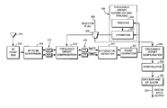
- FIG. 3 is a block diagram showing a first embodiment of the invention, in which frequency offset estimation and tracking are both performed in the phase domain, and in which compensation therefor is also applied in the phase domain.
- an RF signal encoding a data payload is received by antenna 111 , processed by RF front end 112 , and down-converted to a baseband signal by RF-to-BB converter 114 .
- a pair of A-to-D converters 115 convert the analog signals from RF-to-BB converter 114 into digital data, which is thereupon supplied to a pair of low-pass filters 116 and thence to differential detector 117 .
- phase extractor 121 Based on the demodulated PSK signal, phase extractor 121 extracts phase which is provided to frequency offset compensation block 134 so as to correct for frequency offsets, as will be described hereinbelow.
- the frequency offset-compensated signal from block 134 is provided to demodulator 122 and thereafter to decoding and bit-slicing block 124 , so as to result in digital output data 125 corresponding to the digital data payload in the original RF-transmitted signal.
- Frequency offset compensator 134 is provided with an estimate of frequency offset from frequency offset estimation and tracking block 130 .
- block 130 includes an estimation module 131 and a tracking module 132 .
- the purpose of estimation module 131 is to acquire an initial estimate of frequency offset and to provide the acquired estimate to frequency offset compensation block 134 .
- the purpose of tracking block 132 is to determine residual frequency offset errors which might remain after initial acquisition by estimation block 131 , and also to track slowly drifting frequency offsets which might occur because of frequency shifts in the receiver or the transmitter, or which might be caused by fading channel.
- the tracked frequency offset is provided from tracking block 132 to frequency offset compensator 134 via the estimation block 131 , but it is possible for the tracking block 132 to bypass the estimation block 131 and provide an estimate of residual frequency offset directly to compensation block 134 .
- Both estimation block 131 and tracking block 132 work in the phase domain, and provide estimates of frequency offset to compensation block 134 which compensates for frequency offset in the phase domain.
- Estimation block 131 acquires an initial estimate of frequency offset in accordance with the aforementioned equation 4 which is reproduced here:
- phase extraction is always needed in such a DQPSK receiver, it can be shared from phase extraction block 121 and no additional units are needed for this purpose.
- estimation block 131 acquires its initial estimate of frequency offset in a manner that is advantageous relative to conventional systems. For example, because the estimate of frequency offset is acquired in the phase domain, there is ordinarily no need to perform complex-value multiplications and additions as might be needed in conventional systems as represented by Equation 2 above. This lower level of computational complexity translates into smaller chip-area and power consumptions relative to conventional systems. Further, the number of pilots, N, can typically be much less than that used above in Equation 2, since the blind tracking loop followed by tracking block 132 (described below) can further decrease any residual estimation error. Thus, transmission efficiency is further improved using fewer pilots, which translates into a smaller preamble and a larger data payload.
- Equation 1 is generally equal to precisely 1. Due to this, the estimation range for the frequency offset is extended up to half the signal bandwidth, thus assuring a much higher estimation range relative to conventional systems.
- FIG. 4 illustrates this situation.
- FIG. 4 is a representative graph of phase angle of signal 141 versus time over a few symbol periods, with an envelope 142 superimposed on the maximum signals.
- dashed line 143 shows dashed line 143 and which eventually will cause bit errors.
- FIG. 5 shows the operation of tracking block 132 , which tracks these residual frequency offset errors so as to result in a stabilized estimate of frequency offset, even in the presence of residual errors from the initial acquisition, and even in the presence of drift in frequency offset.
- FIG. 5 shows a representative graph of phase angle of signal 151 versus time over a few symbol periods, with an envelope 152 superimposed on the maximum signals.
- tracking block 132 observes the phase envelope of the phase signal so as to ensure that the phase envelope does not exhibit drift caused by frequency offset error.
- tracking block 132 samples the phase signal at points corresponding to maximum and minimum deviations of the envelope.
- Tracking block 132 obtains the average of the maximum and minimum deviations in the phase envelope, and the average corresponds to residual frequency offset and frequency drift. This information is updated to the existing frequency offset estimate in estimation block 131 , which thereupon provides the updated estimate to frequency offset compensation block 134 .
- tracking block 132 to sample the positive and negative phases corresponding to the clocked sampling phases for each symbol, thereby avoiding the cost for searching for the minimum and maximum deviations.
- the sum of these two phases provides a residual frequency offset and frequency drift, and as before, is updated to the existing frequency offset estimate through estimation block 131 and thence to frequency offset compensation block 134 .
- FIG. 6 is a view showing a second embodiment of the invention, in which frequency offset estimation and tracking is performed in the phase domain, as before, but in which compensation is performed in the time domain.
- Reference numerals shown in FIG. 6 are similar to those in FIG. 3 where functionality is also similar, and a description thereof is omitted.
- frequency offset compensation block 213 performs frequency offset compensation in the time domain. Compensation is performed based on an estimate obtained by frequency offset estimation and tracking block 230 , which obtains its estimate of frequency offset in the phase domain in a manner similar to that of block 130 of the first embodiment.
- FIG. 7 A third embodiment of the invention is shown in FIG. 7 in which there is a programmable selection as to whether frequency offset compensation is performed in the phase domain or in the time domain. Like-numbered reference numerals are used in FIG. 7 relative to FIGS. 3 and 6 , for similarly-functioning blocks.
- programmable selector 335 provides the estimate of frequency offset either to a time domain-based compensator 313 or to a phase domain-based compensator 334 . Selection of the destination is programmable in accordance with selector flag 336 .
- FIG. 8 is a generalized flow diagram showing methods performed by the invention herein.
- the process steps shown in FIG. 8 may be carried out by a hardware apparatus embodying the invention, or they may be carried out by software embodying the invention, or in hybrid hardware/software systems.
- the software is ordinarily stored on computer-readable memory media such as ROM or EEPROM which stores computer-executable code which, when executed by a microprocessor or equivalent CPU is executed to carry out such methods.
- step S 801 an RF signal is received which encodes a digital payload.
- the RF signal is processed so as to obtain a demodulated signal (step S 802 ), such as by pre-processing the RF signal to convert the RF signal to an intermediate or broadband signal and thereafter to apply differential detection so as to obtain the demodulated signal.
- Phase is extracted from the demodulated signal (step S 803 ), and in the phase domain, using the extracted phase, an estimate is made of frequency offset (step S 804 ) and/or frequency offset is tracked (step S 805 ).
- a current estimate of frequency offset is then applied in step S 806 so as to compensate the signal for frequency offset.
- compensation for frequency offset can be performed in the phase domain (as depicted in FIG. 8 ) or can be performed in the time domain.
- the ordering of steps S 803 and S 806 is reversed, such that there is a compensation for frequency offset before there is an extraction of phase.
- the current estimation of frequency offset is performed through a feed-back arrangement, rather than the feed-forward arrangement of FIG. 8 .
- steps S 807 through S 809 perform post-processing in order to process the compensated signal to obtain the digital data payload. Specifically, step S 807 demodulates the compensated signal to obtain a demodulated signal that also is compensated for frequency offset. Step S 808 decodes the compensated signal and also performs bit-slicing operation so as to obtain the digital payload, which is thereafter output in step S 809 .
- FIGS. 9 through 13 show additional embodiments of the invention when implemented as part of a wireless LAN (WLAN) in particular applications of WLAN.
- WLAN wireless LAN
- the present invention may be embodied in a high definition television (HDTV) 420 .
- the present invention may implement either or both signal processing and/or control circuits, which are generally identified in FIG. 9 at 422 , a WLAN interface and/or mass data storage of the HDTV 420 .
- HDTV 420 receives HDTV input signals in either a wired or wireless format and generates HDTV output signals for a display 426 .
- signal processing circuit and/or control circuit 422 and/or other circuits (not shown) of HDTV 420 may process data, perform coding and/or encryption, perform calculations, format data and/or perform any other type of HDTV processing that may be required.
- HDTV 420 may communicate with mass data storage 427 that stores data in a nonvolatile manner such as optical and/or magnetic storage devices.
- the HDD may be a mini HDD that includes one or more platters having a diameter that is smaller than approximately 1.8′′.
- HDTV 420 may be connected to memory 428 such as RAM, ROM, low latency nonvolatile memory such as flash memory and/or other suitable electronic data storage.
- HDTV 420 also may support connections with a WLAN via a WLAN network interface 429 .
- the present invention implements a control system of a vehicle 430 , a WLAN interface and/or mass data storage of the vehicle control system.
- the present invention implements a powertrain control system 432 that receives inputs from one or more sensors such as temperature sensors, pressure sensors, rotational sensors, airflow sensors and/or any other suitable sensors and/or that generates one or more output control signals such as engine operating parameters, transmission operating parameters, and/or other control signals.
- control system 440 may likewise receive signals from input sensors 442 and/or output control signals to one or more output devices 444 .
- control system 440 may be part of an anti-lock braking system (ABS), a navigation system, a telematics system, a vehicle telematics system, a lane departure system, an adaptive cruise control system, a vehicle entertainment system such as a stereo, DVD, compact disc and the like. Still other implementations are contemplated.
- ABS anti-lock braking system
- Powertrain control system 432 may communicate with mass data storage 446 that stores data in a nonvolatile manner.
- Mass data storage 446 may include optical and/or magnetic storage devices for example hard disk drives HDD and/or DVDs.
- the HDD may be a mini HDD that includes one or more platters having a diameter that is smaller than approximately 1.8′′.
- Powertrain control system 432 may be connected to memory 447 such as RAM, ROM, low latency nonvolatile memory such as flash memory and/or other suitable electronic data storage.
- Powertrain control system 432 also may support connections with a WLAN via a WLAN network interface 448 .
- the control system 440 may also include mass data storage, memory and/or a WLAN interface (all not shown).
- the present invention may be embodied in a cellular phone 450 that may include a cellular antenna 451 .
- the present invention may implement either or both signal processing and/or control circuits, which are generally identified in FIG. 11 at 452 , a WLAN interface and/or mass data storage of the cellular phone 450 .
- cellular phone 450 includes a microphone 456 , an audio output 458 such as a speaker and/or audio output jack, a display 460 and/or an input device 462 such as a keypad, pointing device, voice actuation and/or other input device.
- Signal processing and/or control circuits 452 and/or other circuits (not shown) in cellular phone 450 may process data, perform coding and/or encryption, perform calculations, format data and/or perform other cellular phone functions.
- Cellular phone 450 may communicate with mass data storage 464 that stores data in a nonvolatile manner such as optical and/or magnetic storage devices for example hard disk drives HDD and/or DVDs.
- the HDD may be a mini HDD that includes one or more platters having a diameter that is smaller than approximately 1.8′′.
- Cellular phone 450 may be connected to memory 466 such as RAM, ROM, low latency nonvolatile memory such as flash memory and/or other suitable electronic data storage.
- Cellular phone 450 also may support connections with a WLAN via a WLAN network interface 468 .
- the present invention may be embodied in a set top box 480 .
- the present invention may implement either or both signal processing and/or control circuits, which are generally identified in FIG. 12 at 484 , a WLAN interface and/or mass data storage of the set top box 480 .
- Set top box 480 receives signals from a source such as a broadband source and outputs standard and/or high definition audio/video signals suitable for a display 488 such as a television and/or monitor and/or other video and/or audio output devices.
- Signal processing and/or control circuits 484 and/or other circuits (not shown) of the set top box 480 may process data, perform coding and/or encryption, perform calculations, format data and/or perform any other set top box function.
- Set top box 480 may communicate with mass data storage 490 that stores data in a nonvolatile manner.
- Mass data storage 490 may include optical and/or magnetic storage devices for example hard disk drives HDD and/or DVDs.
- the HDD may be a mini HDD that includes one or more platters having a diameter that is smaller than approximately 1.8′′.
- Set top box 480 may be connected to memory 494 such as RAM, ROM, low latency nonvolatile memory such as flash memory and/or other suitable electronic data storage.
- Set top box 480 also may support connections with a WLAN via a WLAN network interface 496 .
- the present invention may be embodied in a media player 500 .
- the present invention may implement either or both signal processing and/or control circuits, which are generally identified in FIG. 13 at 504 , a WLAN interface and/or mass data storage of the media player 500 .
- media player 500 includes a display 507 and/or a user input 508 such as a keypad, touchpad and the like.
- media player 500 may employ a graphical user interface (GUI) that typically employs menus, drop down menus, icons and/or a point-and-click interface via display 507 and/or user input 508 .
- Media player 500 further includes an audio output 509 such as a speaker and/or audio output jack.
- Signal processing and/or control circuits 504 and/or other circuits (not shown) of media player 500 may process data, perform coding and/or encryption, perform calculations, format data and/or perform any other media player function.
- Media player 500 may communicate with mass data storage 510 that stores data such as compressed audio and/or video content in a nonvolatile manner.
- the compressed audio files include files that are compliant with MP3 format or other suitable compressed audio and/or video formats.
- the mass data storage may include optical and/or magnetic storage devices for example hard disk drives HDD and/or DVDs.
- the HDD may be a mini HDD that includes one or more platters having a diameter that is smaller than approximately 1.8′′.
- Media player 500 may be connected to memory 514 such as RAM, ROM, low latency nonvolatile memory such as flash memory and/or other suitable electronic data storage.
- Media player 500 also may support connections with a WLAN via a WLAN network interface 516 . Still other implementations in addition to those described above are contemplated
Abstract
Description
y(n)=y di(n)+j*y dq(n)=ae jψ (Equation 1)
where y(n) is the nth symbol, ydi and ydq are the in-phase and quadrature phase demodulated PSK signals, respectively, j is the imaginary coordinate for the complex value, and a and P represent the amplitude and phase of the received signal, respectively. Based on this mathematical notation, frequency offset estimation and
where Δf is the frequency offset, T is time, {circumflex over (ψ)} is the estimate of phase, y(n) is the demodulated PSK signal from
y(n)=y(n−L) (Equation 3)
for n=0, . . . , N−1, which means that the training signals need to be repeated in order to obtain the frequency offset estimate.
where Δf is the frequency offset, T is time, {circumflex over (ψ)} is the estimate of phase, y(n) is the demodulated PSK signal, N is the length of one training block, L represents the distance between two identical samples, and angle (.) indicates the phase extraction operation. Since phase extraction is always needed in such a receiver, it can be shared and no additional units are needed for this purpose.
y(n)=y di(n)+j*y dq(n)=ae jψ (Equation 1)
where y(n) is the nth symbol, ydi and ydq are the in-phase and quadrature phase demodulated PSK signal, j is the imaginary coordinate for the complex value, and a and P represent the amplitude and phase of the receive signal, respectively.
where Δf is the frequency offset, T is time, {circumflex over (ψ)} is the estimate of phase, y(n) is the demodulated PSK signal, N is the length of one training block, L represents the distance between two identical samples, and angle(.) indicates the phase extraction operation. Since phase extraction is always needed in such a DQPSK receiver, it can be shared from
Claims (9)
Priority Applications (2)
| Application Number | Priority Date | Filing Date | Title |
|---|---|---|---|
| US11/500,633 US7809083B1 (en) | 2006-01-23 | 2006-08-08 | Differential receiver with frequency offset compensation |
| US12/893,926 US8139688B1 (en) | 2006-01-23 | 2010-09-29 | Differential receiver with frequency offset compensation |
Applications Claiming Priority (2)
| Application Number | Priority Date | Filing Date | Title |
|---|---|---|---|
| US76124106P | 2006-01-23 | 2006-01-23 | |
| US11/500,633 US7809083B1 (en) | 2006-01-23 | 2006-08-08 | Differential receiver with frequency offset compensation |
Related Child Applications (1)
| Application Number | Title | Priority Date | Filing Date |
|---|---|---|---|
| US12/893,926 Continuation US8139688B1 (en) | 2006-01-23 | 2010-09-29 | Differential receiver with frequency offset compensation |
Publications (1)
| Publication Number | Publication Date |
|---|---|
| US7809083B1 true US7809083B1 (en) | 2010-10-05 |
Family
ID=42797809
Family Applications (2)
| Application Number | Title | Priority Date | Filing Date |
|---|---|---|---|
| US11/500,633 Active 2029-07-03 US7809083B1 (en) | 2006-01-23 | 2006-08-08 | Differential receiver with frequency offset compensation |
| US12/893,926 Active US8139688B1 (en) | 2006-01-23 | 2010-09-29 | Differential receiver with frequency offset compensation |
Family Applications After (1)
| Application Number | Title | Priority Date | Filing Date |
|---|---|---|---|
| US12/893,926 Active US8139688B1 (en) | 2006-01-23 | 2010-09-29 | Differential receiver with frequency offset compensation |
Country Status (1)
| Country | Link |
|---|---|
| US (2) | US7809083B1 (en) |
Cited By (9)
| Publication number | Priority date | Publication date | Assignee | Title |
|---|---|---|---|---|
| US20090111411A1 (en) * | 2007-10-24 | 2009-04-30 | The Trustees Of Princeton University | System and Method for Blind Estimation of Multiple Carrier Frequency Offsets and Separation of User Signals in Wireless Communications Systems |
| US20110103529A1 (en) * | 2009-10-30 | 2011-05-05 | Fujitsu Limited | Estimating Frequency Offset Using A Feedback Loop |
| CN102201824A (en) * | 2010-03-23 | 2011-09-28 | 上海华虹集成电路有限责任公司 | Combined digital down conversion and frequency offset correction circuit and realization method thereof |
| US20120271575A1 (en) * | 2009-09-30 | 2012-10-25 | Alstom Technology Ltd | Phase angle drift method for loss of mains/grid protection |
| WO2013116373A1 (en) * | 2012-01-30 | 2013-08-08 | Qualcomm Incorporated | Multiple correlators for communication device detection |
| US8731029B1 (en) | 2010-01-12 | 2014-05-20 | Marvell International Ltd. | Frequency offset acquisition for wireless communications |
| EP3185500A1 (en) * | 2015-12-23 | 2017-06-28 | Intel IP Corporation | Frequency offset and modulation index estimation for bluetooth low energy ble communication |
| WO2017112072A1 (en) * | 2015-12-22 | 2017-06-29 | Intel Corporation | Joint noncoherent demodulation and carrier frequency offset correction based on non-linear filtering |
| US10476731B2 (en) | 2015-12-22 | 2019-11-12 | Intel Corporation | Joint noncoherent demodulation and carrier frequency offset correction based on non-linear filtering |
Families Citing this family (3)
| Publication number | Priority date | Publication date | Assignee | Title |
|---|---|---|---|---|
| WO2012117374A1 (en) * | 2011-03-03 | 2012-09-07 | Technion R&D Foundation | Coherent and self - coherent signal processing techniques |
| CN103414523B (en) * | 2012-12-14 | 2015-07-22 | 中国计量科学研究院 | Method for measuring modulation quality parameters based on software radio technology and system |
| KR102034221B1 (en) | 2013-03-11 | 2019-10-18 | 삼성전자주식회사 | Semiconductor device including receiver for differentail signal |
Citations (19)
| Publication number | Priority date | Publication date | Assignee | Title |
|---|---|---|---|---|
| US5376894A (en) * | 1992-12-31 | 1994-12-27 | Pacific Communication Sciences, Inc. | Phase estimation and synchronization using a PSK demodulator |
| US5432819A (en) * | 1994-03-09 | 1995-07-11 | Martin Marietta Corporation | DPSK communications with Doppler compensation |
| US5440267A (en) * | 1993-09-14 | 1995-08-08 | Nec Corporation | Demodulator |
| US5581582A (en) * | 1994-03-25 | 1996-12-03 | Samsung Electronics Co., Ltd. | Automatic frequency control method and apparatus therefor |
| US5581572A (en) * | 1994-02-11 | 1996-12-03 | France Telecom | Wavelength-tunable, distributed bragg reflector laser having selectively activated, virtual diffraction gratings |
| US6363126B1 (en) * | 1997-12-12 | 2002-03-26 | Matsushita Electric Industrial Co., Ltd. | Demodulator |
| US6778613B2 (en) * | 1998-03-05 | 2004-08-17 | Agere Systems, Inc. | Frequency and phase estimation for MPSK signals |
| US20040240596A1 (en) | 2000-06-12 | 2004-12-02 | Broadcom Corporation | Receiver architecture employing low intermediate frequency and complex filtering |
| US6882208B1 (en) | 2003-10-22 | 2005-04-19 | Texas Instruments Incorporated | Adjustment of amplitude and DC offsets in a digital receiver |
| US20050085249A1 (en) * | 2003-10-16 | 2005-04-21 | Pctel, Inc. | Method, apparatus and system for pilotless frequency offset compensation in multipoint-to-point wireless systems with OFDM |
| US20050163274A1 (en) | 2003-12-15 | 2005-07-28 | Oki Electric Industry Co., Ltd. | Syncword detecting circuit and a baseband signal receiving circuit |
| US20050164639A1 (en) | 2004-01-27 | 2005-07-28 | Texas Instruments Incorporated | Frequency offset compensation in a digital frequency shift keying receiver |
| US6975691B1 (en) * | 1997-12-17 | 2005-12-13 | Kabushiki Kaisha Kenwood | Receiver |
| US20060133527A1 (en) * | 2004-12-11 | 2006-06-22 | Heejung Yu | Residual frequency, phase, timing offset and signal amplitude variation tracking apparatus and methods for OFDM systems |
| US7224666B2 (en) * | 2002-05-13 | 2007-05-29 | Texas Instruments Incorporated | Estimating frequency offsets using pilot tones in an OFDM system |
| US7305053B2 (en) * | 2001-11-06 | 2007-12-04 | Nxp B.V. | Dat-aided frequency offset detection using phase unwrapping |
| US7392031B2 (en) * | 2003-06-25 | 2008-06-24 | Nxp B.V. | Method for cancelling a narrow-band interference signal |
| US7477707B2 (en) * | 2003-07-10 | 2009-01-13 | Honeywell International Inc. | Computationally efficient demodulation for differential phase shift keying |
| US7675989B2 (en) * | 2005-03-25 | 2010-03-09 | Electronics And Telecommunications Research Institute | Method and apparatus for uplink carrier frequency synchronization and antenna weight vector estimation in OFDMA system having smart antenna |
Family Cites Families (4)
| Publication number | Priority date | Publication date | Assignee | Title |
|---|---|---|---|---|
| US6023491A (en) * | 1994-06-21 | 2000-02-08 | Matsushita Electric Industrail Co., Ltd. | Demodulation apparatus performing different frequency control functions using separately provided oscillators |
| CN1148871C (en) * | 1998-04-17 | 2004-05-05 | 汤姆森特许公司 | LNB drift search system for DBS products |
| US6363123B1 (en) | 1999-02-23 | 2002-03-26 | Leica Geosystems Inc. | Receiver calibration technique for global orbiting navigation satellite system (GLONASS) |
| US6590945B1 (en) * | 1999-07-13 | 2003-07-08 | Lucent Technologies Inc. | Method and apparatus for frequency offset compensation |
-
2006
- 2006-08-08 US US11/500,633 patent/US7809083B1/en active Active
-
2010
- 2010-09-29 US US12/893,926 patent/US8139688B1/en active Active
Patent Citations (20)
| Publication number | Priority date | Publication date | Assignee | Title |
|---|---|---|---|---|
| US5625652A (en) | 1992-12-31 | 1997-04-29 | Pacific Communication Sciences, Inc. | Timing recovery controller and method for adjusting the timing of synchronizing windows in a PSK demodulator |
| US5376894A (en) * | 1992-12-31 | 1994-12-27 | Pacific Communication Sciences, Inc. | Phase estimation and synchronization using a PSK demodulator |
| US5440267A (en) * | 1993-09-14 | 1995-08-08 | Nec Corporation | Demodulator |
| US5581572A (en) * | 1994-02-11 | 1996-12-03 | France Telecom | Wavelength-tunable, distributed bragg reflector laser having selectively activated, virtual diffraction gratings |
| US5432819A (en) * | 1994-03-09 | 1995-07-11 | Martin Marietta Corporation | DPSK communications with Doppler compensation |
| US5581582A (en) * | 1994-03-25 | 1996-12-03 | Samsung Electronics Co., Ltd. | Automatic frequency control method and apparatus therefor |
| US6363126B1 (en) * | 1997-12-12 | 2002-03-26 | Matsushita Electric Industrial Co., Ltd. | Demodulator |
| US6975691B1 (en) * | 1997-12-17 | 2005-12-13 | Kabushiki Kaisha Kenwood | Receiver |
| US6778613B2 (en) * | 1998-03-05 | 2004-08-17 | Agere Systems, Inc. | Frequency and phase estimation for MPSK signals |
| US20040240596A1 (en) | 2000-06-12 | 2004-12-02 | Broadcom Corporation | Receiver architecture employing low intermediate frequency and complex filtering |
| US7305053B2 (en) * | 2001-11-06 | 2007-12-04 | Nxp B.V. | Dat-aided frequency offset detection using phase unwrapping |
| US7224666B2 (en) * | 2002-05-13 | 2007-05-29 | Texas Instruments Incorporated | Estimating frequency offsets using pilot tones in an OFDM system |
| US7392031B2 (en) * | 2003-06-25 | 2008-06-24 | Nxp B.V. | Method for cancelling a narrow-band interference signal |
| US7477707B2 (en) * | 2003-07-10 | 2009-01-13 | Honeywell International Inc. | Computationally efficient demodulation for differential phase shift keying |
| US20050085249A1 (en) * | 2003-10-16 | 2005-04-21 | Pctel, Inc. | Method, apparatus and system for pilotless frequency offset compensation in multipoint-to-point wireless systems with OFDM |
| US6882208B1 (en) | 2003-10-22 | 2005-04-19 | Texas Instruments Incorporated | Adjustment of amplitude and DC offsets in a digital receiver |
| US20050163274A1 (en) | 2003-12-15 | 2005-07-28 | Oki Electric Industry Co., Ltd. | Syncword detecting circuit and a baseband signal receiving circuit |
| US20050164639A1 (en) | 2004-01-27 | 2005-07-28 | Texas Instruments Incorporated | Frequency offset compensation in a digital frequency shift keying receiver |
| US20060133527A1 (en) * | 2004-12-11 | 2006-06-22 | Heejung Yu | Residual frequency, phase, timing offset and signal amplitude variation tracking apparatus and methods for OFDM systems |
| US7675989B2 (en) * | 2005-03-25 | 2010-03-09 | Electronics And Telecommunications Research Institute | Method and apparatus for uplink carrier frequency synchronization and antenna weight vector estimation in OFDMA system having smart antenna |
Non-Patent Citations (3)
| Title |
|---|
| "Information technology-Telecommunications and information exchange between systems-Local and metropolitan area networks-Specific requirements-Part 11: Wireless LAN Medium Access Control (MAC) and Physical Layer (PHY) specifications" International Standard ISO/IEC 8802-11, ANSI/IEEE Std. 802.11, 1999. |
| M. Morelli, et al., "Further Results in Carrier Frequency Estimation for Transmissions Over Flat Fading Channels", IEEE Communications Letters, vol. 2, No. 12, Dec. 1998, pp. 327-330. |
| O. Besson, et al., "On Frequency Offset Estimation for Flat-Fading Channels", IEEE Communications Letters, vol. 5, No. 10, Oct. 2001, pp. 402-404. |
Cited By (16)
| Publication number | Priority date | Publication date | Assignee | Title |
|---|---|---|---|---|
| US20090111411A1 (en) * | 2007-10-24 | 2009-04-30 | The Trustees Of Princeton University | System and Method for Blind Estimation of Multiple Carrier Frequency Offsets and Separation of User Signals in Wireless Communications Systems |
| US7929937B2 (en) * | 2007-10-24 | 2011-04-19 | The Trustees Of Princeton University | System and method for blind estimation of multiple carrier frequency offsets and separation of user signals in wireless communications systems |
| US9325175B2 (en) * | 2009-09-30 | 2016-04-26 | Alstom Technology Ltd. | Phase angle drift method for loss of mains/grid protection |
| US20120271575A1 (en) * | 2009-09-30 | 2012-10-25 | Alstom Technology Ltd | Phase angle drift method for loss of mains/grid protection |
| US20110103529A1 (en) * | 2009-10-30 | 2011-05-05 | Fujitsu Limited | Estimating Frequency Offset Using A Feedback Loop |
| US8335438B2 (en) * | 2009-10-30 | 2012-12-18 | Fujitsu Limited | Estimating frequency offset using a feedback loop |
| US8731029B1 (en) | 2010-01-12 | 2014-05-20 | Marvell International Ltd. | Frequency offset acquisition for wireless communications |
| US9356648B1 (en) | 2010-01-12 | 2016-05-31 | Marvell International Ltd. | Frequency offset acquisition for wireless communications |
| CN102201824B (en) * | 2010-03-23 | 2013-12-04 | 上海华虹集成电路有限责任公司 | Realization method of combined digital down conversion and frequency offset correction circuit |
| CN102201824A (en) * | 2010-03-23 | 2011-09-28 | 上海华虹集成电路有限责任公司 | Combined digital down conversion and frequency offset correction circuit and realization method thereof |
| WO2013116373A1 (en) * | 2012-01-30 | 2013-08-08 | Qualcomm Incorporated | Multiple correlators for communication device detection |
| US8824606B2 (en) | 2012-01-30 | 2014-09-02 | Qualcomm Incorporated | Multiple correlators for communication device detection |
| WO2017112072A1 (en) * | 2015-12-22 | 2017-06-29 | Intel Corporation | Joint noncoherent demodulation and carrier frequency offset correction based on non-linear filtering |
| US10476731B2 (en) | 2015-12-22 | 2019-11-12 | Intel Corporation | Joint noncoherent demodulation and carrier frequency offset correction based on non-linear filtering |
| EP3185500A1 (en) * | 2015-12-23 | 2017-06-28 | Intel IP Corporation | Frequency offset and modulation index estimation for bluetooth low energy ble communication |
| US9722845B2 (en) | 2015-12-23 | 2017-08-01 | Intel IP Corporation | Bluetooth low energy frequency offset and modulation index estimation |
Also Published As
| Publication number | Publication date |
|---|---|
| US8139688B1 (en) | 2012-03-20 |
Similar Documents
| Publication | Publication Date | Title |
|---|---|---|
| US7809083B1 (en) | Differential receiver with frequency offset compensation | |
| US8027414B2 (en) | Carrier frequency recovering apparatus using phase shift and method thereof | |
| US20050259768A1 (en) | Digital receiver and method for processing received signals | |
| US7801249B2 (en) | Carrier phase and symbol timing recovery circuit for an ATSC receiver and method of recovering a carrier phase and a symbol timing in received digital signal data | |
| US7639750B2 (en) | Phase tracking method and device thereof | |
| US8218696B2 (en) | Receiving apparatus, receiving method, integrated circuit, digital television receiver, and program | |
| JP2002511711A (en) | Method and apparatus for fine frequency synchronization in a multi-carrier demodulation system | |
| US7298806B1 (en) | Method and system for data-aided timing offset estimation for frequency selective fading channels | |
| US8611472B2 (en) | Carrier frequency offset estimation scheme, for digital standards with MPSK modulated preamble | |
| JP2008005357A (en) | Dc offset removing apparatus and dc offset removing method | |
| US7415078B2 (en) | Demodulation for phase modulation | |
| US7529179B1 (en) | Joint maximum likelihood estimation of integer carrier frequency offset and channel in OFDM systems | |
| JP2008530951A (en) | Demodulator and receiver for pre-encoded partial response signals | |
| US7664210B2 (en) | Non-coherent synchronous direct-conversion receiving apparatus for compensating frequency offset | |
| US8792591B1 (en) | Systems and methods for I/Q imbalance correction and calibration of variable modulus signals | |
| US7760819B2 (en) | Digital wireless receiver | |
| US8194768B1 (en) | Channel estimation using linear phase estimation | |
| US9350587B1 (en) | System and method for timing error estimation | |
| US8155216B2 (en) | Receiving circuit and receiving method | |
| US8804877B2 (en) | Apparatus and method for correcting phase error | |
| CN115632923A (en) | OQPSK (offset quadrature phase shift keying) -based unmanned aerial vehicle and satellite ultra-wideband communication method and related equipment | |
| US8295402B2 (en) | Optimal blind channel estimation for DQPSK demodulation | |
| WO2022172327A1 (en) | Transmission device, reception device, communication system, control circuit, storage medium, transmission method, and reception method | |
| GB2524464A (en) | Frequency error estimation | |
| KR20070000274A (en) | Apparatus and method of bpsk/qpsk blind modulation classification in wireless communication system |
Legal Events
| Date | Code | Title | Description |
|---|---|---|---|
| AS | Assignment |
Owner name: MARVELL SEMICONDUCTOR, INC., CALIFORNIA Free format text: ASSIGNMENT OF ASSIGNORS INTEREST;ASSIGNORS:WU, SONGPING;LOU, HUI-LING;REEL/FRAME:018150/0315 Effective date: 20060803 Owner name: MARVELL INTERNATIONAL LTD., BERMUDA Free format text: ASSIGNMENT OF ASSIGNORS INTEREST;ASSIGNOR:MARVELL SEMICONDUCTOR, INC.;REEL/FRAME:018150/0311 Effective date: 20060808 |
|
| STCF | Information on status: patent grant |
Free format text: PATENTED CASE |
|
| FPAY | Fee payment |
Year of fee payment: 4 |
|
| MAFP | Maintenance fee payment |
Free format text: PAYMENT OF MAINTENANCE FEE, 8TH YEAR, LARGE ENTITY (ORIGINAL EVENT CODE: M1552) Year of fee payment: 8 |
|
| AS | Assignment |
Owner name: NXP USA, INC., TEXAS Free format text: ASSIGNMENT OF ASSIGNORS INTEREST;ASSIGNOR:MARVELL INTERNATIONAL LTD.;REEL/FRAME:051536/0001 Effective date: 20191206 |
|
| MAFP | Maintenance fee payment |
Free format text: PAYMENT OF MAINTENANCE FEE, 12TH YEAR, LARGE ENTITY (ORIGINAL EVENT CODE: M1553); ENTITY STATUS OF PATENT OWNER: LARGE ENTITY Year of fee payment: 12 |