US7808015B2 - Apparatus comprising an avalanche photodiode - Google Patents
Apparatus comprising an avalanche photodiode Download PDFInfo
- Publication number
- US7808015B2 US7808015B2 US12/051,650 US5165008A US7808015B2 US 7808015 B2 US7808015 B2 US 7808015B2 US 5165008 A US5165008 A US 5165008A US 7808015 B2 US7808015 B2 US 7808015B2
- Authority
- US
- United States
- Prior art keywords
- region
- edge
- active
- photodiode
- width
- Prior art date
- Legal status (The legal status is an assumption and is not a legal conclusion. Google has not performed a legal analysis and makes no representation as to the accuracy of the status listed.)
- Active, expires
Links
- 230000015556 catabolic process Effects 0.000 claims abstract description 37
- 230000003287 optical effect Effects 0.000 claims abstract description 28
- 239000002019 doping agent Substances 0.000 claims description 78
- 238000009792 diffusion process Methods 0.000 claims description 75
- 239000004065 semiconductor Substances 0.000 claims description 62
- 239000000969 carrier Substances 0.000 claims description 4
- 238000000098 azimuthal photoelectron diffraction Methods 0.000 abstract description 30
- 230000008878 coupling Effects 0.000 abstract description 9
- 238000010168 coupling process Methods 0.000 abstract description 9
- 238000005859 coupling reaction Methods 0.000 abstract description 9
- 230000007547 defect Effects 0.000 abstract description 8
- 238000013461 design Methods 0.000 abstract description 5
- 238000001514 detection method Methods 0.000 description 12
- 238000000034 method Methods 0.000 description 12
- 238000010521 absorption reaction Methods 0.000 description 11
- 230000005684 electric field Effects 0.000 description 9
- 239000000463 material Substances 0.000 description 8
- GPXJNWSHGFTCBW-UHFFFAOYSA-N Indium phosphide Chemical compound [In]#P GPXJNWSHGFTCBW-UHFFFAOYSA-N 0.000 description 7
- 238000005468 ion implantation Methods 0.000 description 6
- 238000004519 manufacturing process Methods 0.000 description 6
- 230000015572 biosynthetic process Effects 0.000 description 5
- 229910052581 Si3N4 Inorganic materials 0.000 description 3
- 230000004888 barrier function Effects 0.000 description 3
- 239000013078 crystal Substances 0.000 description 3
- 230000000694 effects Effects 0.000 description 3
- 230000002028 premature Effects 0.000 description 3
- HQVNEWCFYHHQES-UHFFFAOYSA-N silicon nitride Chemical compound N12[Si]34N5[Si]62N3[Si]51N64 HQVNEWCFYHHQES-UHFFFAOYSA-N 0.000 description 3
- 238000007669 thermal treatment Methods 0.000 description 3
- OKTJSMMVPCPJKN-UHFFFAOYSA-N Carbon Chemical compound [C] OKTJSMMVPCPJKN-UHFFFAOYSA-N 0.000 description 2
- NINIDFKCEFEMDL-UHFFFAOYSA-N Sulfur Chemical compound [S] NINIDFKCEFEMDL-UHFFFAOYSA-N 0.000 description 2
- HCHKCACWOHOZIP-UHFFFAOYSA-N Zinc Chemical compound [Zn] HCHKCACWOHOZIP-UHFFFAOYSA-N 0.000 description 2
- 238000013459 approach Methods 0.000 description 2
- 229910052790 beryllium Inorganic materials 0.000 description 2
- ATBAMAFKBVZNFJ-UHFFFAOYSA-N beryllium atom Chemical compound [Be] ATBAMAFKBVZNFJ-UHFFFAOYSA-N 0.000 description 2
- 229910052793 cadmium Inorganic materials 0.000 description 2
- BDOSMKKIYDKNTQ-UHFFFAOYSA-N cadmium atom Chemical compound [Cd] BDOSMKKIYDKNTQ-UHFFFAOYSA-N 0.000 description 2
- 229910052799 carbon Inorganic materials 0.000 description 2
- 238000004891 communication Methods 0.000 description 2
- 230000003247 decreasing effect Effects 0.000 description 2
- 238000005530 etching Methods 0.000 description 2
- 238000000206 photolithography Methods 0.000 description 2
- 238000001020 plasma etching Methods 0.000 description 2
- 230000008569 process Effects 0.000 description 2
- 230000009467 reduction Effects 0.000 description 2
- 230000004044 response Effects 0.000 description 2
- 229910052710 silicon Inorganic materials 0.000 description 2
- 239000010703 silicon Substances 0.000 description 2
- 238000004544 sputter deposition Methods 0.000 description 2
- 238000000992 sputter etching Methods 0.000 description 2
- 229910052717 sulfur Inorganic materials 0.000 description 2
- 239000011593 sulfur Substances 0.000 description 2
- 238000001039 wet etching Methods 0.000 description 2
- 229910052725 zinc Inorganic materials 0.000 description 2
- 239000011701 zinc Substances 0.000 description 2
- 229910000530 Gallium indium arsenide Inorganic materials 0.000 description 1
- KXNLCSXBJCPWGL-UHFFFAOYSA-N [Ga].[As].[In] Chemical compound [Ga].[As].[In] KXNLCSXBJCPWGL-UHFFFAOYSA-N 0.000 description 1
- 230000007423 decrease Effects 0.000 description 1
- 238000005516 engineering process Methods 0.000 description 1
- 238000012423 maintenance Methods 0.000 description 1
- 230000007246 mechanism Effects 0.000 description 1
- 230000006911 nucleation Effects 0.000 description 1
- 238000010899 nucleation Methods 0.000 description 1
- 239000000758 substrate Substances 0.000 description 1
Images


Classifications
-
- H—ELECTRICITY
- H01—ELECTRIC ELEMENTS
- H01L—SEMICONDUCTOR DEVICES NOT COVERED BY CLASS H10
- H01L31/00—Semiconductor devices sensitive to infrared radiation, light, electromagnetic radiation of shorter wavelength or corpuscular radiation and specially adapted either for the conversion of the energy of such radiation into electrical energy or for the control of electrical energy by such radiation; Processes or apparatus specially adapted for the manufacture or treatment thereof or of parts thereof; Details thereof
- H01L31/08—Semiconductor devices sensitive to infrared radiation, light, electromagnetic radiation of shorter wavelength or corpuscular radiation and specially adapted either for the conversion of the energy of such radiation into electrical energy or for the control of electrical energy by such radiation; Processes or apparatus specially adapted for the manufacture or treatment thereof or of parts thereof; Details thereof in which radiation controls flow of current through the device, e.g. photoresistors
- H01L31/10—Semiconductor devices sensitive to infrared radiation, light, electromagnetic radiation of shorter wavelength or corpuscular radiation and specially adapted either for the conversion of the energy of such radiation into electrical energy or for the control of electrical energy by such radiation; Processes or apparatus specially adapted for the manufacture or treatment thereof or of parts thereof; Details thereof in which radiation controls flow of current through the device, e.g. photoresistors characterised by at least one potential-jump barrier or surface barrier, e.g. phototransistors
- H01L31/101—Devices sensitive to infrared, visible or ultraviolet radiation
- H01L31/102—Devices sensitive to infrared, visible or ultraviolet radiation characterised by only one potential barrier or surface barrier
- H01L31/107—Devices sensitive to infrared, visible or ultraviolet radiation characterised by only one potential barrier or surface barrier the potential barrier working in avalanche mode, e.g. avalanche photodiode
- H01L31/1075—Devices sensitive to infrared, visible or ultraviolet radiation characterised by only one potential barrier or surface barrier the potential barrier working in avalanche mode, e.g. avalanche photodiode in which the active layers, e.g. absorption or multiplication layers, form an heterostructure, e.g. SAM structure
Definitions
- the present invention relates to avalanche photodiodes in general and, more particularly, to avalanche photodiodes for use in single-photon detection applications.
- Avalanche photodiode (APD) structures that have separate absorption and multiplication layers can provide electrical output signals with high fidelity (i.e., low noise).
- SAM-APD the optical energy is absorbed and converted into electrical carriers in a layer specifically designed for efficient absorption (hereinafter, referred to as the “absorption layer”).
- the resulting electrical signal is amplified in a different layer specifically designed for efficient electrical carrier multiplication (hereinafter, referred to as the “cap layer”).
- a device region can be formed in the cap layer of a SAM-APD by diffusion of a dopant into the semiconductor layer to form a p-n junction.
- the undoped portion of the cap layer that resides beneath the p-n junction provides a high-field region in which avalanche multiplication can occur (i.e., the avalanche multiplication region).
- the principal driver for improved APD performance has been its use in telecommunications systems.
- the APD is electrically biased such that the electrical response is substantially linear with optical power.
- the APD is electrically biased at or beyond its “electrical breakdown voltage.”
- the breakdown voltage is the voltage at which the p-n junction is sufficiently reverse-biased to conduct a large current arising from a self-sustaining avalanche process—even in the absence of continuous optical power.
- An APD that is biased at or above breakdown therefore, can give rise to an easily detectable pulse of electrical current in response to the absorption of even a single photon.
- Gain and breakdown voltage are functions of the thickness of the undoped portion of the device region.
- Dopant diffusion in a semiconductor is a substantially isotropic process (i.e., the dopant diffuses laterally and vertically, at nearly the same rate).
- active region central portion
- edge region outer portion
- the active region is characterized by a uniform, planar junction profile while the edge region has a non-uniform, curved junction profile.
- the uniform junction profile leads to uniform gain and uniform breakdown voltage.
- the curvature of the junction profile in the edge region leads to a larger local electric field and therefore higher gain and lower breakdown voltage than in the active region. This undesirable phenomenon is typically referred to as “edge breakdown”.
- the breakdown-voltage uniformity across the entire device region should be within 10%, and preferably within 1%.
- NEP Noise Equivalent Power
- a low NEP can be achieved by 1) high detection efficiency and/or 2) low dark count rate.
- Detection efficiency is a function of several factors: (i) the amount of the light signal which is directed into the detector (i.e., optical coupling efficiency); (ii) the probability that a received photon is absorbed by the detector (i.e., quantum efficiency); and (iii) the probability that the absorbed photon will result in a detectable avalanche event (i.e., avalanche probability).
- a high coupling efficiency can be achieved by making the device region of an APD at least as large as the mode-field diameter of the optical beam.
- Many prior art photodiodes in fact, have a device region that is larger than the mode-field diameter so as to both capture as much of the light as possible and allow for some misalignment while still capturing the entire beam.
- Avalanche probability can be improved by increasing the bias voltage so that it is well above the breakdown voltage.
- the larger this overbias the greater the probability that a received photon will generate an avalanche event.
- dark count rate also increases with overbias; therefore in many cases increased overbias actually degrades NEP rather than improves it.
- the present invention is an avalanche photodiode having separate multiplication and absorption layers (SAM-APDs).
- SAM-APDs separate multiplication and absorption layers
- the avalanche photodiode provides high optical coupling efficiency and low dark count rate.
- Some embodiments of the present invention are particularly useful for single-photon detection applications.
- An aspect of the present invention is the inventors' recognition that the dark count rate is a function of the number of defects located in the device region of an APD, and that the dark count rate can be decreased by reducing the volume of the device region. In some embodiments, the total volume of the device region is reduced by decreasing the width of the edge region. APDs of these embodiments still maintain a uniform gain profile or a uniform breakdown voltage profile across the device region.
- a further aspect of the present invention is the recognition that the curvature of the junction profile in the edge region (and therefore the gain and breakdown voltage in the edge region) is affected by the ratio of certain parameters of the APD, as follows:
- FIG. 1 depicts a SAM avalanche photodiode in communication with an optical beam according to an embodiment of the present invention.
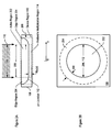
- FIG. 2A depicts a cross-sectional view of an optical beam coupled to the cap layer of a SAM-APD according to an embodiment of the present invention.
- FIG. 2B depicts a top view of an optical beam coupled to the cap layer of a SAM-APD according to an embodiment of the present invention.
- FIG. 3A depicts a cross-sectional view of a cap layer of a SAM-APD, formed using a single dopant diffusion, according to the prior art.
- FIG. 3B depicts a cross-sectional view of a cap layer of a SAM-APD, formed using a single dopant diffusion, according to an embodiment of the present invention.
- FIG. 4 depicts the salient components of a single diffusion method for fabricating the cap layer of a SAM-APD in accordance with an embodiment of the present invention.
- FIGS. 5A through 5C depict cross-sectional views of a cap layer during proceeding stages of fabrication, as fabricated in accordance with the operations depicted in FIG. 4 .
- FIG. 6A depicts a cross-sectional view of a cap layer of a SAM-APD, formed with a double diffusion, according to the prior art.
- FIG. 6B depicts a cross-sectional view of a cap layer of a SAM-APD, formed with a double diffusion, according to an embodiment of the present invention.
- FIG. 7 depicts the salient components of a double diffusion method for fabricating the cap layer of a SAM-APD in accordance with an embodiment of the present invention.
- FIGS. 8A through 8D depict cross-sectional views of a cap layer during proceeding stages of fabrication, as fabricated in accordance with the operations depicted in FIG. 7 .
- a low NEP is of particular importance.
- a photodiode with low NEP contributes few false signals while still detecting many or most received photons.
- a low NEP can be achieved by 1) high detection efficiency, and/or 2) low dark count rate.
- the desire for high detection efficiency and low dark count rate leads to a conflict in design methodology.
- the device region of the APD is large so as to couple all of the energy contained in the mode-field diameter of the optical beam being detected.
- the dark count rate is proportional to the size of the device region, and therefore it is desirable to make the device area small.
- APDs in accordance with the illustrative embodiment have a reduced device-region volume. This is accomplished by reducing the width of the edge region, while avoiding premature edge breakdown.
- FIG. 1 depicts a SAM avalanche photodiode receiving an optical beam according to an embodiment of the present invention.
- Photodiode 100 comprises substrate 102 , absorption layer 104 , charge control layer 106 , and cap layer 108 .
- Absorption layer 104 absorbs the optical energy of optical beam 116 , as contained within mode-field diameter 118 , and generates electrical carriers.
- Absorption layer 104 is an intrinsic layer of indium gallium arsenide. It will be clear to those skilled in the art how to make and use absorption layer 104 .
- Charge control layer 106 is a moderately n-doped layer of indium phosphide. Charge control layer 106 enables maintenance of a low electric field in absorption layer 104 , while supporting a high electric field in cap layer 108 . It will be clear to those skilled in the art how to make and use charge control layer 106 .
- Cap layer 108 is a lightly n-doped layer of indium phosphide.
- the terms “lightly n-doped” and “lightly p-doped” refer to the intentional doping of a semiconductor layer with an n-type or p-type dopant to a dopant concentration of less than three orders of magnitude greater than the background concentration of the semiconductor layer.
- device region 110 which includes a heavily doped p-type region.
- Device region 110 is formed by diffusing a p-type dopant into cap layer 108 to form p-n junction 112 .
- the lateral extent of p-n junction 112 defines the lateral extent of device region 110 .
- avalanche multiplication region 114 which is a high-field multiplication region of thickness W m (x) in which avalanche multiplication occurs.
- W m ( 0 ) is a value in the range from 2% to 50% of the thickness of cap layer 108 . In some embodiments, W m ( 0 ) is a value between 10-25% of the thickness of cap layer 108 . In some embodiments, W m ( 0 ) is approximately 20% of the thickness of cap layer 108 .
- cap layer 108 is a lightly p-doped layer of indium phosphide and device region 110 is heavily doped with an n-type dopant. In some other embodiments, cap layer 108 is an intrinsic layer of III-V semiconductor material. It will be clear to those skilled in the art, after reading this specification, how to make and use embodiments of the present invention in which cap layer 108 is other than a lightly n-doped layer of indium phosphide.
- FIGS. 2A and 2B depict a cross-sectional view and top view, respectively, of an optical beam coupled to the cap layer of a SAM-APD according to an embodiment of the present invention.
- Cap layer 108 comprises device region 110 , which is defined laterally by the extent of p-n junction 112 .
- Device region 110 comprises active region 202 , having active-region width 206 , and edge region 204 , having edge-region width 208 .
- Active region 202 is the central portion of device region 110 wherein p-n junction 112 is at a uniform depth (i.e., where p-n junction 112 is a plane junction).
- the value of W m (x) is substantially equal to W m ( 0 ) across active-region width 206 .
- active-region width 206 is substantially equal to mode-field diameter 118 of optical beam 116 .
- active-region width 206 is made larger than mode-field diameter 118 in order to facilitate optical coupling to optical beam 116 .
- Edge region 204 is the outer region of device region 110 , wherein p-n junction 112 is non-planar. Edge region 204 is formed by the lateral diffusion of the dopant used to form p-n junction 112 , as will be described below and with respect to FIGS. 5A through 5C . In edge region 204 , the value of W m (x) and the profile of p-n junction 112 vary with x. In some embodiments, p-n junction 112 forms a quasi-cylindrical junction in edge region 204 . In some embodiments, p-n junction 112 forms a quasi-spherical junction in edge region 204 .
- active region 202 is a circular region surrounded by annular edge region 204 .
- active region 202 is non-circular.
- edge region 204 takes the form of a larger annulus of substantially the same outline with substantially uniform width.
- FIG. 3A depicts a cross-sectional view of a cap layer of a SAM-APD, formed using a single dopant diffusion, according to the prior art.
- Cap layer 300 comprises semiconductor layer 302 and doped region 304 .
- Doped region 304 is a heavily p-doped region within n-doped semiconductor layer 302 , and forms p-n junction 306 .
- Doped region 304 includes a planar junction region (i.e., an active region) having active-region width 308 , and a cylindrical junction region (i.e., an edge region) having edge-region width 310 .
- the junction depth of p-n junction 306 in the active region is approximately equal to diffusion radius r j .
- Active region width 308 is much larger than edge-region width 310 and is also much larger than diffusion radius r j .
- Avalanche gain, breakdown field, and breakdown voltage are all substantially uniform in the planar junction region, as denoted by the uniform space between equipotential electric field lines 312 in this region.
- the cylindrical junction nature of the edge region gives rise to the well-known junction curvature effect.
- the junction curvature effect leads to a higher electric field intensity and lower breakdown voltage in the edge region (commonly referred to as “edge breakdown”), as denoted by the crowding of equipotential field lines 312 in regions 314 .
- the effect of junction curvature on breakdown voltage is derived from Poisson's equation as:
- V e V a 2 ⁇ ( ⁇ 2 + 2 ⁇ ⁇ 6 / 7 ) ⁇ ln ⁇ ( 1 + 2 ⁇ ⁇ - 8 / 7 ) - ⁇ 6 / 7 [ 1 ]
- a number of approaches for limiting edge breakdown are known in the prior art. These include: 1) adding guard rings outside the junction area to control the doping density at the junction edges; 2) adding a shaped charge control layer underneath the cap layer to enhance the electric field in the active region; and 3) forming a multi-tiered doping profile to reduce the curvature (and therefore the induced local electric field) of the junction profile at the edge of the device region.
- Common to all these approaches is an enlarged device region and/or more complicated device fabrication, which can lead to lower device yield, higher device cost, and lower device reliability.
- An aspect of the present invention is the recognition that the curvature of the junction profile in the edge region is affected by several factors:
- the curvature of the junction profile affects the intensity of the electric field in the edge region, and, as a result, the edge-region breakdown voltage.
- the present invention therefore, provides APD structures with specific relationships between:
- the mode-field diameter of the optical beam to which the APD is to be coupled may be small.
- the required active-region width could be small enough that the device region could be formed using a single dopant diffusion while still avoiding premature edge breakdown.
- the present invention therefore, provides for APDs with device regions formed using a single diffusion.
- the mode-field diameter of the optical beam to which the APD is to be coupled is larger.
- a larger active region is required for efficient optical coupling.
- multiple diffusions typically, two
- the relative sizes of the multiple diffusion regions have been determined, however, on the basis of avoidance of edge breakdown and without regard to the size of the device region as a whole. Therefore, optical coupling efficiency has been pursued without concern for dark count rate.
- the width of the edge region with respect to other design parameters is carefully considered as one of the relationships outlined above. The relative importance of each of these relationships, however, can differ between the single-diffusion case and multiple diffusion case. Therefore, the single-diffusion case and multiple diffusion case are addressed separately below.
- FIG. 3B depicts a cross-sectional view of a cap layer of a SAM-APD, formed using a single dopant diffusion, according to an embodiment of the present invention.
- Cap layer 108 comprises semiconductor layer 316 and doped region 318 .
- Semiconductor layer 316 is a lightly n-doped layer of indium phosphide having a layer thickness of T c .
- Doped region 318 is a heavily p-doped region within semiconductor layer 316 , which forms p-n junction 112 .
- P-n junction 112 includes a planar junction region (i.e., active region 202 ) having active-region width 206 and a cylindrical junction region (i.e., edge region 204 ) having edge-region width 208 .
- semiconductor layer 316 is an intrinsic semiconductor layer.
- doped region 318 is doped with either an n-type dopant or a p-type dopant.
- semiconductor layer 316 is a lightly p-doped semiconductor and doped region 318 is doped with an n-type dopant.
- doped region 318 is formed by diffusing a single p-type dopant into semiconductor layer 316 using a single diffusion process.
- the p-type dopant diffuses into semiconductor layer 316 to a diffusion radius of approximately R de .
- the junction profile is planar and the junction depth of doped region 318 is substantially equal to R de .
- the junction profile is that of a cylindrical junction having a radius of curvature of approximately R de .
- the lateral diffusion rate of a dopant in a semiconductor sometimes differs from the vertical diffusion rate.
- the junction depth may differ slightly from R de , even in the case of a single diffusion of a single dopant.
- a slight difference in lateral and vertical diffusion rates is neglected, since it is not pertinent to the scope of the invention.
- multiple p-type dopants are diffused into semiconductor layer 316 in a single process.
- the local values of gain and breakdown voltage are functions of the localized electric field and, therefore, are affected by the relationship between active-region width 206 and edge-region width 208 .
- the crowding of equipotential lines 320 becomes excessive as active region width 206 is made larger than twice the diffusion radius, R de (for example, cap layer 302 of FIG. 3A ).
- R de for example, cap layer 302 of FIG. 3A
- the resultant reduction in breakdown voltage therefore, also becomes excessive and the APD ceases to function properly.
- R de for example, cap layer 302 of FIG. 3A
- active region width is substantially equal to R de .
- edge-region width 208 is approximately equal to R de
- active-region width 206 can be expressed as a function of edge-region width 208 , wherein active-region width 206 is in the range of approximately 0.5 to 2 times edge-region width 208 .
- Diffusion radius R de (and, therefore, the junction depth in active region 202 ) is chosen to provide a suitable avalanche gain in active region 202 .
- R de is in the range of 0.5T c to 0.98T c .
- R de is in the range of 0.75T c to 0.9T c .
- R de is approximately 0.8T c .
- active-region width 206 can be expressed as a function of T c , wherein active-region width 206 is in the range of approximately 0.25T c to approximately 2T c .
- FIG. 4 depicts the salient components of a single diffusion method for fabricating the cap layer of a SAM-APD in accordance with an embodiment of the present invention.
- method 400 is used to form cap layer 108 shown in FIG. 3B .
- cap layer 108 As depicted in FIG. 3B , the formation of cap layer 108 , as depicted in FIG. 3B , will be described in conjunction with FIGS. 5A-C .
- FIGS. 5A-C depict cross-sectional views of cap layer 108 at various stages of fabrication.
- a first mask-layer opening on a semiconductor layer is provided, as depicted in FIG. 5A .
- mask-layer opening 502 is formed in mask layer 504 .
- Mask layer 504 is a 200 nm-thick film of silicon nitride deposited on semiconductor layer 316 .
- Mask layer 504 is suitable for providing a diffusion barrier to p-type dopants.
- Mask-layer opening 502 is formed in mask layer 504 using conventional photolithography and reactive ion etching. Other suitable means for forming mask-layer opening 502 include wet-etching, ion milling, sputtering, and laser-assisted etching. It will be clear to those skilled in the art how to make and use mask-layer opening 502 and mask layer 504 .
- p-type dopant 506 is diffused into semiconductor layer 316 through mask-layer opening 502 , as depicted in FIG. 5B .
- Suitable p-type dopants include, without limitation, zinc, cadmium, beryllium, and carbon.
- dopant 506 diffuses both vertically and laterally into semiconductor layer 316 , and forms diffusion front 508 .
- the diffusion front in active region 202 forms as a planar front that progresses downward vertically into semiconductor layer 316 .
- Lateral diffusion of dopant atoms at the edges of mask-layer opening 504 leads to the formation of edge region 204 .
- the profile of diffusion front 508 in edge region is dictated by the classical diffusion equation.
- p-type dopant 506 is implanted into semiconductor layer 316 using ion-implantation. In some embodiments, ion-implantation is followed by a thermal treatment at an elevated temperature to drive the implanted dopant further into semiconductor layer 316 .
- diffusion front 508 and p-n junction 112 extend laterally past the edges of mask-layer opening 502 by the distance equal to diffusion radius R de , thereby forming edge regions 204 .
- the depth of p-n junction 112 is substantially equal to diffusion radius R de .
- semiconductor layer 316 is a p-type semiconductor and dopant 506 is an n-type dopant.
- Suitable n-type dopants include, without limitation, sulfur and silicon.
- FIG. 6A depicts a cross-sectional view of a cap layer of a SAM-APD, formed using a double diffusion, according to the prior art.
- Cap layer 600 comprises semiconductor layer 602 and doped region 604 .
- Semiconductor layer 602 is a lightly n-doped layer of indium phosphide.
- Doped region 604 is a heavily p-doped region within semiconductor layer 602 , and forms p-n junction 606 .
- Doped region 604 includes a planar junction region (i.e., an active region) having an active-region width and a non-planar junction region (i.e., an edge region) having an edge-region width.
- Doped region 604 is formed using two diffusion operations and therefore includes two diffusion fronts, first diffusion front 608 and second diffusion front 610 .
- the junction profile of p-n junction 606 is a function of both R da and R de .
- R de is the diffusion radius of a first p-type dopant and R da is the diffusion radius of a second p-type dopant.
- edge-region width is often made quite wide to avoid premature edge breakdown near the active region.
- a wider edge region creates a more smoothly varying junction profile in the edge region and improves edge breakdown conditions.
- FIG. 6B depicts a cross-sectional view of a cap layer of a SAM-APD, formed using a double diffusion, according to an embodiment of the present invention.
- Cap layer 612 comprises semiconductor layer 614 and doped region 616 .
- Semiconductor layer 602 is a lightly n-doped layer of indium phosphide having thickness T c .
- Doped region 616 is a heavily p-doped region within semiconductor layer 614 , and forms p-n junction 618 .
- Doped region 616 includes a planar junction region (i.e., active region 202 ) having active-region width 206 and a non-planar junction region (i.e., edge region 204 ) having edge-region width 208 .
- Avalanche multiplication occurs in the high-electric field, undoped portion of active area 202 .
- semiconductor layer 614 is an intrinsic semiconductor layer.
- doped region 616 is doped with either an n-type dopant or a p-type dopant.
- semiconductor layer 614 is a lightly p-doped semiconductor and doped region 616 is doped with an n-type dopant.
- doped region 616 is formed by two diffusions of a p-type dopant into semiconductor layer 614 .
- First diffusion front 620 is a function of the diffusion radius, R de , of a first dopant and the diffusion radius, R da , of a second dopant.
- Second diffusion front 622 is at a distance equal to the diffusion radius, R da , of a second dopant.
- the lateral extent of active region 202 is defined by the portion of second diffusion front which is at uniform depth (i.e., the planar junction region of p-n junction 618 ).
- the lateral extent of edge region 204 is defined by the outer portion of p-n junction 618 that is not at uniform depth.
- edge-region width 208 is in the range of approximately R de +1 ⁇ 2R da to R de +2R da . In some embodiments, edge-region width 208 is substantially equal to R de +R da .
- the first dopant is the same as the second dopant.
- R da is equal to R de . It will be noted by those skilled in the art that the lateral and vertical diffusion rates of a dopant in a semiconductor are sometimes not equal. For the purposes of this specification, however, R da and R de will be treated as uniform in the lateral and vertical directions.
- FIG. 7 depicts the salient components of a double diffusion method for fabricating the cap layer of a SAM-APD in accordance with an embodiment of the present invention.
- method 700 is used to form cap layer 612 shown in FIG. 6B .
- cap layer 612 As depicted in FIG. 6B , will be described in conjunction with the cross-sectional views of cap layer 800 at various stages of fabrication depicted in FIGS. 8A-D .
- first mask-layer opening 802 is formed in first mask layer 804 .
- the width of first mask-layer opening 802 is first mask-layer opening width 806 .
- First mask layer 804 is a 200 nm-thick film of silicon nitride deposited on semiconductor layer 614 , and is suitable for providing a diffusion barrier to p-type dopants.
- First mask-layer opening 802 is formed in first mask layer 804 using conventional photolithography and reactive ion etching.
- first mask-layer opening 802 Other suitable means for forming first mask-layer opening 802 include wet-etching, ion milling, sputtering, and laser-assisted etching. It will be clear to those skilled in the art, after reading this specification, how to form and use first mask-layer opening 802 .
- p-type dopant 808 is diffused into semiconductor layer 614 through mask-layer opening 802 , thereby forming first diffusion front 620 , as depicted in FIG. 8B .
- dopant 808 diffuses both laterally and vertically into semiconductor layer 614 as shown.
- Suitable p-type dopants include, without limitation, zinc, cadmium, beryllium, and carbon.
- p-type dopant 808 is implanted into semiconductor layer 614 using ion-implantation. In some embodiments, ion-implantation is followed by a thermal treatment at an elevated temperature to drive dopant 808 further into semiconductor layer 614 .
- second mask-layer opening 810 is formed in second mask layer 812 .
- Second mask-layer 812 is a 200 nm-thick film of silicon nitride, and is suitable for providing a diffusion barrier to p-type dopants.
- Second mask-layer opening 810 is smaller than first mask-layer opening 802 by an amount in the range of approximately R da to approximately 4R da . In some embodiments, second mask-layer opening 810 is smaller than first mask-layer opening 802 by approximately 2R da .
- second p-type dopant 816 is diffused into semiconductor layer 614 through second mask-layer opening 810 , thereby forming second diffusion front 622 . Due to the heat associated with the diffusion of second p-type dopant 816 , first diffusion front 620 progresses further into semiconductor layer 614 during operation 704 .
- operation 704 comprises the ion implantation of second dopant 816 into semiconductor layer 614 .
- ion-implantation is followed by a thermal treatment at an elevated temperature to drive dopant 816 into semiconductor layer 614 to diffusion radius R da and to drive dopant 808 into semiconductor layer 614 to diffusion radius R de .
- diffusion front 620 and p-n junction 618 extend laterally past the edges of second mask-layer opening 810 by a distance that is a function of diffusion radii R da and R de , and thereby form edge regions 204 .
- Edge-region width 208 is a function of R da and R de , wherein edge-region width 208 is in the range of approximately R de +1 ⁇ 2R da to approximately R de +2R da .
- the depth of p-n junction 618 is also a function of diffusion radii R da and R de and is in the range of approximately 0.5T c to approximately 0.98T c .
- second mask-layer opening 810 and first mask-layer opening are both formed in first mask layer 804 .
- second mask-layer opening 810 is formed prior to first mask-layer opening 802 .
- semiconductor layer 614 is a p-type semiconductor and first dopant 808 and second dopant 816 are n-type dopants.
- Suitable n-type dopants include, without limitation, sulfur and silicon.
Abstract
Description
-
- an active region of sufficient width for high coupling efficiency with an optical beam; and
- an edge region, wherein the width of the edge region is substantially minimized, and wherein gain and breakdown voltage in the edge region are within approximately 10% of the gain and breakdown voltage, respectively, in the active region.
-
- edge-region width to active region width;
- edge-region width to the diffusion radius of the dopants in the edge region;
- edge-region width to cap layer thickness.
Some embodiments of APDs described herein fall within a desired range of the foregoing ratios. Such APDs operate with low NEP while maintaining a uniform gain profile or uniform breakdown voltage across the device region.
-
- Device region is the portion of the cap layer defined by the lateral extent of the doped portion of the cap layer. The device region includes the full thickness of the cap layer, and therefore includes the undoped portion of the cap layer that resides under the doped portion. For example, the device region includes both the active region and the edge region, as defined below.
- Active region means that portion of the cap layer wherein the p-n junction has a substantially uniform doping profile and junction depth (i.e., wherein the p-n junction is a planar junction). The active region extends though the entire thickness of the cap layer, and therefore also includes the avalanche multiplication region under the planar junction.
- Edge region means that portion of the cap layer wherein the p-n junction does not have a substantially uniform doping profile and junction depth (i.e., wherein the p-n junction is spherical or cylindrical). The edge region extends through the entire thickness of the cap layer. In APD designs that include guard rings, the edge region includes those areas of the cap layer that are doped to form the guard ring structures.
-
- Ve is the edge-region breakdown voltage;
- Va is the active-region breakdown voltage; and
- η is a function of the radius of curvature of the junction in the edge region, rj.
-
- i. edge-region width with respect to active region width; or
- ii. edge-region width with respect to the diffusion radius of the dopants in the edge region; or
- iii. edge-region width with respect to cap layer thickness; or
- iv. any combination of i, ii, and iii.
-
- a. the active-region width and the edge-region width; or
- b. the diffusion radius of the dopant in the active region and edge-region width; or
- c. the active-region width and the thickness of the cap layer; or
- d. the edge-region width and the diffusion radii of the dopants in the active and edge regions; or
- e. the edge-region width and the thickness of the cap layer; or
- f. any combination of a, b, c, d, and e.
Claims (19)
Priority Applications (1)
| Application Number | Priority Date | Filing Date | Title |
|---|---|---|---|
| US12/051,650 US7808015B2 (en) | 2005-10-17 | 2008-03-19 | Apparatus comprising an avalanche photodiode |
Applications Claiming Priority (2)
| Application Number | Priority Date | Filing Date | Title |
|---|---|---|---|
| US11/251,965 US7378689B2 (en) | 2005-10-17 | 2005-10-17 | Apparatus comprising an avalanche photodiode |
| US12/051,650 US7808015B2 (en) | 2005-10-17 | 2008-03-19 | Apparatus comprising an avalanche photodiode |
Related Parent Applications (1)
| Application Number | Title | Priority Date | Filing Date |
|---|---|---|---|
| US11/251,965 Division US7378689B2 (en) | 2005-10-17 | 2005-10-17 | Apparatus comprising an avalanche photodiode |
Publications (2)
| Publication Number | Publication Date |
|---|---|
| US20080164554A1 US20080164554A1 (en) | 2008-07-10 |
| US7808015B2 true US7808015B2 (en) | 2010-10-05 |
Family
ID=37947380
Family Applications (3)
| Application Number | Title | Priority Date | Filing Date |
|---|---|---|---|
| US11/251,965 Active 2026-03-01 US7378689B2 (en) | 2005-10-17 | 2005-10-17 | Apparatus comprising an avalanche photodiode |
| US12/051,650 Active 2026-08-20 US7808015B2 (en) | 2005-10-17 | 2008-03-19 | Apparatus comprising an avalanche photodiode |
| US12/051,651 Active US7582920B2 (en) | 2005-10-17 | 2008-03-19 | Apparatus comprising an avalanche photodiode |
Family Applications Before (1)
| Application Number | Title | Priority Date | Filing Date |
|---|---|---|---|
| US11/251,965 Active 2026-03-01 US7378689B2 (en) | 2005-10-17 | 2005-10-17 | Apparatus comprising an avalanche photodiode |
Family Applications After (1)
| Application Number | Title | Priority Date | Filing Date |
|---|---|---|---|
| US12/051,651 Active US7582920B2 (en) | 2005-10-17 | 2008-03-19 | Apparatus comprising an avalanche photodiode |
Country Status (1)
| Country | Link |
|---|---|
| US (3) | US7378689B2 (en) |
Cited By (1)
| Publication number | Priority date | Publication date | Assignee | Title |
|---|---|---|---|---|
| US20090204381A1 (en) * | 2008-02-13 | 2009-08-13 | Feng Ma | Simulation Methods and Systems for Carriers Having Multiplications |
Families Citing this family (9)
| Publication number | Priority date | Publication date | Assignee | Title |
|---|---|---|---|---|
| JP5015494B2 (en) * | 2006-05-22 | 2012-08-29 | 住友電工デバイス・イノベーション株式会社 | Semiconductor photo detector |
| US7834379B2 (en) * | 2007-07-18 | 2010-11-16 | Jds Uniphase Corporation | Avalanche photodiode with edge breakdown suppression |
| EP2073277A1 (en) * | 2007-12-19 | 2009-06-24 | Alcatel Lucent | Avalanche photodiode |
| GB2456149B (en) * | 2008-01-03 | 2012-05-30 | Toshiba Res Europ Ltd | A photon detection system and a method of photon detection |
| WO2014172697A1 (en) | 2013-04-19 | 2014-10-23 | Lightspin Technologies, Inc. | Integrated avalanche photodiode arrays |
| CN103531465B (en) * | 2013-09-13 | 2018-04-06 | 上海集成电路研发中心有限公司 | fast recovery diode preparation method |
| WO2016178678A1 (en) | 2015-05-06 | 2016-11-10 | Lightspin Technologies, Inc. | Integrated avalanche photodiode arrays |
| CN105070780B (en) * | 2015-07-30 | 2017-03-01 | 中国电子科技集团公司第四十四研究所 | A kind of plane three ladder knot avalanche photodide and manufacture method |
| US10529884B2 (en) | 2017-11-09 | 2020-01-07 | LightSpin Technologies Inc. | Virtual negative bevel and methods of isolating adjacent devices |
Citations (10)
| Publication number | Priority date | Publication date | Assignee | Title |
|---|---|---|---|---|
| US4634474A (en) | 1984-10-09 | 1987-01-06 | At&T Bell Laboratories | Coating of III-V and II-VI compound semiconductors |
| US5500376A (en) | 1994-04-29 | 1996-03-19 | General Electric Company | Method for fabricating planar avalanche photodiode array |
| US5998837A (en) | 1995-06-02 | 1999-12-07 | Siliconix Incorporated | Trench-gated power MOSFET with protective diode having adjustable breakdown voltage |
| US20020185695A1 (en) | 2001-06-08 | 2002-12-12 | Beasom James Douglas | Lateral DMOS structure with lateral extension structure for reduced charge trapping in gate oxide |
| US6515315B1 (en) | 1999-08-05 | 2003-02-04 | Jds Uniphase, Corp. | Avalanche photodiode for high-speed applications |
| US20030047752A1 (en) | 2000-09-29 | 2003-03-13 | Campbell Joe C. | Avalanche photodiodes with an impact-ionization-engineered multiplication region |
| US6583482B2 (en) | 2000-12-06 | 2003-06-24 | Alexandre Pauchard | Hetero-interface avalance photodetector |
| US6720588B2 (en) | 2001-11-28 | 2004-04-13 | Optonics, Inc. | Avalanche photodiode for photon counting applications and method thereof |
| US20060084187A1 (en) | 2004-10-15 | 2006-04-20 | Francis Daniel A | Starved source diffusion for avalanche photodiode |
| US20060121683A1 (en) | 2004-12-08 | 2006-06-08 | Finisar Corporation | Point source diffusion for avalanche photodiodes |
-
2005
- 2005-10-17 US US11/251,965 patent/US7378689B2/en active Active
-
2008
- 2008-03-19 US US12/051,650 patent/US7808015B2/en active Active
- 2008-03-19 US US12/051,651 patent/US7582920B2/en active Active
Patent Citations (11)
| Publication number | Priority date | Publication date | Assignee | Title |
|---|---|---|---|---|
| US4634474A (en) | 1984-10-09 | 1987-01-06 | At&T Bell Laboratories | Coating of III-V and II-VI compound semiconductors |
| US5500376A (en) | 1994-04-29 | 1996-03-19 | General Electric Company | Method for fabricating planar avalanche photodiode array |
| US5998837A (en) | 1995-06-02 | 1999-12-07 | Siliconix Incorporated | Trench-gated power MOSFET with protective diode having adjustable breakdown voltage |
| US6515315B1 (en) | 1999-08-05 | 2003-02-04 | Jds Uniphase, Corp. | Avalanche photodiode for high-speed applications |
| US20030047752A1 (en) | 2000-09-29 | 2003-03-13 | Campbell Joe C. | Avalanche photodiodes with an impact-ionization-engineered multiplication region |
| US6583482B2 (en) | 2000-12-06 | 2003-06-24 | Alexandre Pauchard | Hetero-interface avalance photodetector |
| US20020185695A1 (en) | 2001-06-08 | 2002-12-12 | Beasom James Douglas | Lateral DMOS structure with lateral extension structure for reduced charge trapping in gate oxide |
| US6720588B2 (en) | 2001-11-28 | 2004-04-13 | Optonics, Inc. | Avalanche photodiode for photon counting applications and method thereof |
| US6797581B2 (en) | 2001-11-28 | 2004-09-28 | Credence Systems Corporation | Avalanche photodiode for photon counting applications and method thereof |
| US20060084187A1 (en) | 2004-10-15 | 2006-04-20 | Francis Daniel A | Starved source diffusion for avalanche photodiode |
| US20060121683A1 (en) | 2004-12-08 | 2006-06-08 | Finisar Corporation | Point source diffusion for avalanche photodiodes |
Non-Patent Citations (7)
| Title |
|---|
| Campbell et al., "Frequency Response of InP/InGaAsP/InGaAs Avalanche Photodiodes with Separate Absorption 'Grading' and Multiplication Reg", "IEEE Journal of Quantum Electronics", Nov. 11, 1985, pp. 1743-1746, vol. QE-21, No. 11, Published in: US. |
| Final Office Action from U.S. Appl. No. 11/251,965 dated Oct. 30, 2007. |
| Menz, Douglas M, "U.S. Appl. No. 11/251,965 Notice of Allowance", Feb. 5, 2008, Publisher: USPTO, Published in: US. |
| Menz, Douglas M., "U.S. Appl. No. 12/051,651 Notice of Allowance", Mar. 24, 2009, Publisher: USPTO, Published in: US. |
| Office Action from U.S. Appl. No. 11/251,965 dated Jun. 29, 2007. |
| Office Action from U.S. Appl. No. 11/251,965 dated May 1, 2007. |
| Y. Liu et al., "A Planar InP/InGaAs Avalanche Photodiode with Floating Guard Ring and Doublt Diffused Junction", "Journal of Lightwave Technology", Feb. 2, 1992, pp. 182-193, vol. 10, No. 2, Published in: US. |
Cited By (2)
| Publication number | Priority date | Publication date | Assignee | Title |
|---|---|---|---|---|
| US20090204381A1 (en) * | 2008-02-13 | 2009-08-13 | Feng Ma | Simulation Methods and Systems for Carriers Having Multiplications |
| US8239176B2 (en) * | 2008-02-13 | 2012-08-07 | Feng Ma | Simulation methods and systems for carriers having multiplications |
Also Published As
| Publication number | Publication date |
|---|---|
| US20080164554A1 (en) | 2008-07-10 |
| US20070085158A1 (en) | 2007-04-19 |
| US7582920B2 (en) | 2009-09-01 |
| US7378689B2 (en) | 2008-05-27 |
| US20080164555A1 (en) | 2008-07-10 |
Similar Documents
| Publication | Publication Date | Title |
|---|---|---|
| US7808015B2 (en) | Apparatus comprising an avalanche photodiode | |
| US7348608B2 (en) | Planar avalanche photodiode | |
| US6359293B1 (en) | Integrated optoelectronic device with an avalanche photodetector and method of making the same using commercial CMOS processes | |
| US9847441B2 (en) | Doped multiplier avalanche photodiode | |
| US9425341B2 (en) | P-I-N photodiode with dopant diffusion barrier layer | |
| US20090020782A1 (en) | Avalanche Photodiode With Edge Breakdown Suppression | |
| US8227882B2 (en) | Light-sensitive component with increased blue sensitivity, method for the production thereof, and operating method | |
| JP2010135360A (en) | Avalanche photodiode | |
| CN113921646B (en) | Single-photon detector, manufacturing method thereof and single-photon detector array | |
| CA2873841C (en) | Planar avalanche photodiode | |
| EP1470574B9 (en) | High speed pin photodiode with increased responsivity | |
| US6730979B2 (en) | Recessed p-type region cap layer avalanche photodiode | |
| CA2564218A1 (en) | Planar avalanche photodiode | |
| US7553734B2 (en) | Method for forming an avalanche photodiode | |
| CN114899267A (en) | Photoelectric conversion device, sensing apparatus, electronic apparatus, and manufacturing method | |
| US6787818B2 (en) | Diffused junction photodetector and fabrication technique | |
| CN114762131A (en) | Avalanche photodiode | |
| US11967664B2 (en) | Photodiodes with serpentine shaped electrical junction | |
| KR20070015602A (en) | Planar avalanche photodiode | |
| CN115621352A (en) | Semiconductor device and method for manufacturing the same | |
| JPS6373676A (en) | Semiconductor photodetector | |
| CN116565040A (en) | Epitaxial structure of high-speed photoelectric detector | |
| Zimmermann et al. | SiGe Photodetectors | |
| Duan et al. | Ge/Si avalanche photodetectors with high gain-bandwidth product | |
| Schneider et al. | Photodetectors |
Legal Events
| Date | Code | Title | Description |
|---|---|---|---|
| AS | Assignment |
Owner name: PRINCETON LIGHTWAVE, INC., NEW JERSEY Free format text: ASSIGNMENT OF ASSIGNORS INTEREST;ASSIGNORS:ITZLER, MARK ALLEN;BEN-MICHAEL, RAFAEL;REEL/FRAME:021405/0661 Effective date: 20080815 |
|
| STCF | Information on status: patent grant |
Free format text: PATENTED CASE |
|
| FPAY | Fee payment |
Year of fee payment: 4 |
|
| FEPP | Fee payment procedure |
Free format text: ENTITY STATUS SET TO UNDISCOUNTED (ORIGINAL EVENT CODE: BIG.) |
|
| MAFP | Maintenance fee payment |
Free format text: PAYMENT OF MAINTENANCE FEE, 8TH YEAR, LARGE ENTITY (ORIGINAL EVENT CODE: M1552) Year of fee payment: 8 |
|
| AS | Assignment |
Owner name: PRINCETON LIGHTWAVE, LLC, NEW JERSEY Free format text: CHANGE OF NAME;ASSIGNOR:PRINCETON LIGHTWAVE, INC.;REEL/FRAME:046349/0820 Effective date: 20180201 |
|
| AS | Assignment |
Owner name: ARGO AI, LLC, PENNSYLVANIA Free format text: ASSIGNMENT OF ASSIGNORS INTEREST;ASSIGNOR:PRINCETON LIGHTWAVE, LLC;REEL/FRAME:046077/0307 Effective date: 20180612 |
|
| MAFP | Maintenance fee payment |
Free format text: PAYMENT OF MAINTENANCE FEE, 12TH YEAR, LARGE ENTITY (ORIGINAL EVENT CODE: M1553); ENTITY STATUS OF PATENT OWNER: LARGE ENTITY Year of fee payment: 12 |
|
| AS | Assignment |
Owner name: LG INNOTEK CO., LTD., KOREA, REPUBLIC OF Free format text: ASSIGNMENT OF ASSIGNORS INTEREST;ASSIGNOR:ARGO AI, LLC;REEL/FRAME:063311/0079 Effective date: 20230404 |