US7807582B2 - Method of forming contacts for a memory device - Google Patents
Method of forming contacts for a memory device Download PDFInfo
- Publication number
- US7807582B2 US7807582B2 US11/368,898 US36889806A US7807582B2 US 7807582 B2 US7807582 B2 US 7807582B2 US 36889806 A US36889806 A US 36889806A US 7807582 B2 US7807582 B2 US 7807582B2
- Authority
- US
- United States
- Prior art keywords
- hard mask
- layer
- mask layer
- insulating material
- openings
- Prior art date
- Legal status (The legal status is an assumption and is not a legal conclusion. Google has not performed a legal analysis and makes no representation as to the accuracy of the status listed.)
- Active, expires
Links
- 238000000034 method Methods 0.000 title claims abstract description 181
- 230000008569 process Effects 0.000 claims abstract description 105
- 238000005530 etching Methods 0.000 claims abstract description 93
- 239000011810 insulating material Substances 0.000 claims abstract description 74
- 238000003860 storage Methods 0.000 claims abstract description 60
- 230000036961 partial effect Effects 0.000 claims abstract description 44
- 230000009977 dual effect Effects 0.000 claims abstract description 32
- 239000010410 layer Substances 0.000 claims description 263
- 239000000463 material Substances 0.000 claims description 23
- 230000002093 peripheral effect Effects 0.000 claims description 21
- 239000003990 capacitor Substances 0.000 claims description 19
- 239000000758 substrate Substances 0.000 claims description 18
- 229910052581 Si3N4 Inorganic materials 0.000 claims description 8
- VYPSYNLAJGMNEJ-UHFFFAOYSA-N Silicium dioxide Chemical compound O=[Si]=O VYPSYNLAJGMNEJ-UHFFFAOYSA-N 0.000 claims description 8
- 229920002120 photoresistant polymer Polymers 0.000 claims description 8
- HQVNEWCFYHHQES-UHFFFAOYSA-N silicon nitride Chemical compound N12[Si]34N5[Si]62N3[Si]51N64 HQVNEWCFYHHQES-UHFFFAOYSA-N 0.000 claims description 8
- 238000000151 deposition Methods 0.000 claims description 7
- 239000006117 anti-reflective coating Substances 0.000 claims description 4
- 235000012239 silicon dioxide Nutrition 0.000 claims description 4
- 239000000377 silicon dioxide Substances 0.000 claims description 4
- 229910052799 carbon Inorganic materials 0.000 claims description 3
- OKTJSMMVPCPJKN-UHFFFAOYSA-N Carbon Chemical compound [C] OKTJSMMVPCPJKN-UHFFFAOYSA-N 0.000 claims description 2
- XUIMIQQOPSSXEZ-UHFFFAOYSA-N Silicon Chemical compound [Si] XUIMIQQOPSSXEZ-UHFFFAOYSA-N 0.000 claims description 2
- 239000005380 borophosphosilicate glass Substances 0.000 claims description 2
- 229910052710 silicon Inorganic materials 0.000 claims description 2
- 239000010703 silicon Substances 0.000 claims description 2
- 239000002356 single layer Substances 0.000 claims 5
- 239000000203 mixture Substances 0.000 claims 3
- 230000000873 masking effect Effects 0.000 description 16
- 239000004020 conductor Substances 0.000 description 10
- 230000015572 biosynthetic process Effects 0.000 description 9
- 239000003989 dielectric material Substances 0.000 description 8
- 238000004519 manufacturing process Methods 0.000 description 8
- 238000012545 processing Methods 0.000 description 6
- WFKWXMTUELFFGS-UHFFFAOYSA-N tungsten Chemical compound [W] WFKWXMTUELFFGS-UHFFFAOYSA-N 0.000 description 6
- 229910052721 tungsten Inorganic materials 0.000 description 6
- 239000010937 tungsten Substances 0.000 description 6
- 229910052751 metal Inorganic materials 0.000 description 5
- 239000002184 metal Substances 0.000 description 5
- 238000005498 polishing Methods 0.000 description 5
- -1 e.g. Substances 0.000 description 4
- RTAQQCXQSZGOHL-UHFFFAOYSA-N Titanium Chemical compound [Ti] RTAQQCXQSZGOHL-UHFFFAOYSA-N 0.000 description 3
- 238000005229 chemical vapour deposition Methods 0.000 description 3
- 238000000206 photolithography Methods 0.000 description 3
- 229910021420 polycrystalline silicon Inorganic materials 0.000 description 3
- 229920005591 polysilicon Polymers 0.000 description 3
- 239000004065 semiconductor Substances 0.000 description 3
- 239000000126 substance Substances 0.000 description 3
- 239000010936 titanium Substances 0.000 description 3
- 229910052719 titanium Inorganic materials 0.000 description 3
- 230000008901 benefit Effects 0.000 description 2
- 238000011161 development Methods 0.000 description 2
- 238000010586 diagram Methods 0.000 description 2
- 238000012986 modification Methods 0.000 description 2
- 230000004048 modification Effects 0.000 description 2
- 150000004767 nitrides Chemical class 0.000 description 2
- 238000000623 plasma-assisted chemical vapour deposition Methods 0.000 description 2
- BOTDANWDWHJENH-UHFFFAOYSA-N Tetraethyl orthosilicate Chemical compound CCO[Si](OCC)(OCC)OCC BOTDANWDWHJENH-UHFFFAOYSA-N 0.000 description 1
- 238000004140 cleaning Methods 0.000 description 1
- 238000004891 communication Methods 0.000 description 1
- 230000002860 competitive effect Effects 0.000 description 1
- 238000010276 construction Methods 0.000 description 1
- 238000013500 data storage Methods 0.000 description 1
- 230000008021 deposition Effects 0.000 description 1
- 238000005137 deposition process Methods 0.000 description 1
- 238000013461 design Methods 0.000 description 1
- 230000005611 electricity Effects 0.000 description 1
- 230000006870 function Effects 0.000 description 1
- 238000010438 heat treatment Methods 0.000 description 1
- 238000005468 ion implantation Methods 0.000 description 1
- 238000002955 isolation Methods 0.000 description 1
- 238000007517 polishing process Methods 0.000 description 1
- 230000002829 reductive effect Effects 0.000 description 1
- 230000004044 response Effects 0.000 description 1
- 229910021332 silicide Inorganic materials 0.000 description 1
- FVBUAEGBCNSCDD-UHFFFAOYSA-N silicide(4-) Chemical compound [Si-4] FVBUAEGBCNSCDD-UHFFFAOYSA-N 0.000 description 1
- 125000006850 spacer group Chemical group 0.000 description 1
- 230000003068 static effect Effects 0.000 description 1
Images


Classifications
-
- H—ELECTRICITY
- H10—SEMICONDUCTOR DEVICES; ELECTRIC SOLID-STATE DEVICES NOT OTHERWISE PROVIDED FOR
- H10B—ELECTRONIC MEMORY DEVICES
- H10B12/00—Dynamic random access memory [DRAM] devices
- H10B12/30—DRAM devices comprising one-transistor - one-capacitor [1T-1C] memory cells
- H10B12/31—DRAM devices comprising one-transistor - one-capacitor [1T-1C] memory cells having a storage electrode stacked over the transistor
- H10B12/315—DRAM devices comprising one-transistor - one-capacitor [1T-1C] memory cells having a storage electrode stacked over the transistor with the capacitor higher than a bit line
-
- H—ELECTRICITY
- H01—ELECTRIC ELEMENTS
- H01L—SEMICONDUCTOR DEVICES NOT COVERED BY CLASS H10
- H01L21/00—Processes or apparatus adapted for the manufacture or treatment of semiconductor or solid state devices or of parts thereof
- H01L21/70—Manufacture or treatment of devices consisting of a plurality of solid state components formed in or on a common substrate or of parts thereof; Manufacture of integrated circuit devices or of parts thereof
- H01L21/71—Manufacture of specific parts of devices defined in group H01L21/70
- H01L21/768—Applying interconnections to be used for carrying current between separate components within a device comprising conductors and dielectrics
- H01L21/76801—Applying interconnections to be used for carrying current between separate components within a device comprising conductors and dielectrics characterised by the formation and the after-treatment of the dielectrics, e.g. smoothing
- H01L21/76802—Applying interconnections to be used for carrying current between separate components within a device comprising conductors and dielectrics characterised by the formation and the after-treatment of the dielectrics, e.g. smoothing by forming openings in dielectrics
-
- H—ELECTRICITY
- H01—ELECTRIC ELEMENTS
- H01L—SEMICONDUCTOR DEVICES NOT COVERED BY CLASS H10
- H01L21/00—Processes or apparatus adapted for the manufacture or treatment of semiconductor or solid state devices or of parts thereof
- H01L21/02—Manufacture or treatment of semiconductor devices or of parts thereof
- H01L21/04—Manufacture or treatment of semiconductor devices or of parts thereof the devices having potential barriers, e.g. a PN junction, depletion layer or carrier concentration layer
- H01L21/18—Manufacture or treatment of semiconductor devices or of parts thereof the devices having potential barriers, e.g. a PN junction, depletion layer or carrier concentration layer the devices having semiconductor bodies comprising elements of Group IV of the Periodic Table or AIIIBV compounds with or without impurities, e.g. doping materials
- H01L21/30—Treatment of semiconductor bodies using processes or apparatus not provided for in groups H01L21/20 - H01L21/26
- H01L21/31—Treatment of semiconductor bodies using processes or apparatus not provided for in groups H01L21/20 - H01L21/26 to form insulating layers thereon, e.g. for masking or by using photolithographic techniques; After treatment of these layers; Selection of materials for these layers
- H01L21/3105—After-treatment
- H01L21/311—Etching the insulating layers by chemical or physical means
- H01L21/31144—Etching the insulating layers by chemical or physical means using masks
-
- H—ELECTRICITY
- H01—ELECTRIC ELEMENTS
- H01L—SEMICONDUCTOR DEVICES NOT COVERED BY CLASS H10
- H01L21/00—Processes or apparatus adapted for the manufacture or treatment of semiconductor or solid state devices or of parts thereof
- H01L21/70—Manufacture or treatment of devices consisting of a plurality of solid state components formed in or on a common substrate or of parts thereof; Manufacture of integrated circuit devices or of parts thereof
- H01L21/71—Manufacture of specific parts of devices defined in group H01L21/70
- H01L21/768—Applying interconnections to be used for carrying current between separate components within a device comprising conductors and dielectrics
- H01L21/76801—Applying interconnections to be used for carrying current between separate components within a device comprising conductors and dielectrics characterised by the formation and the after-treatment of the dielectrics, e.g. smoothing
- H01L21/76829—Applying interconnections to be used for carrying current between separate components within a device comprising conductors and dielectrics characterised by the formation and the after-treatment of the dielectrics, e.g. smoothing characterised by the formation of thin functional dielectric layers, e.g. dielectric etch-stop, barrier, capping or liner layers
- H01L21/76831—Applying interconnections to be used for carrying current between separate components within a device comprising conductors and dielectrics characterised by the formation and the after-treatment of the dielectrics, e.g. smoothing characterised by the formation of thin functional dielectric layers, e.g. dielectric etch-stop, barrier, capping or liner layers in via holes or trenches, e.g. non-conductive sidewall liners
-
- H—ELECTRICITY
- H01—ELECTRIC ELEMENTS
- H01L—SEMICONDUCTOR DEVICES NOT COVERED BY CLASS H10
- H01L21/00—Processes or apparatus adapted for the manufacture or treatment of semiconductor or solid state devices or of parts thereof
- H01L21/70—Manufacture or treatment of devices consisting of a plurality of solid state components formed in or on a common substrate or of parts thereof; Manufacture of integrated circuit devices or of parts thereof
- H01L21/71—Manufacture of specific parts of devices defined in group H01L21/70
- H01L21/768—Applying interconnections to be used for carrying current between separate components within a device comprising conductors and dielectrics
- H01L21/76897—Formation of self-aligned vias or contact plugs, i.e. involving a lithographically uncritical step
-
- H—ELECTRICITY
- H01—ELECTRIC ELEMENTS
- H01L—SEMICONDUCTOR DEVICES NOT COVERED BY CLASS H10
- H01L23/00—Details of semiconductor or other solid state devices
- H01L23/52—Arrangements for conducting electric current within the device in operation from one component to another, i.e. interconnections, e.g. wires, lead frames
- H01L23/522—Arrangements for conducting electric current within the device in operation from one component to another, i.e. interconnections, e.g. wires, lead frames including external interconnections consisting of a multilayer structure of conductive and insulating layers inseparably formed on the semiconductor body
- H01L23/532—Arrangements for conducting electric current within the device in operation from one component to another, i.e. interconnections, e.g. wires, lead frames including external interconnections consisting of a multilayer structure of conductive and insulating layers inseparably formed on the semiconductor body characterised by the materials
- H01L23/53204—Conductive materials
- H01L23/53209—Conductive materials based on metals, e.g. alloys, metal silicides
- H01L23/53257—Conductive materials based on metals, e.g. alloys, metal silicides the principal metal being a refractory metal
- H01L23/53266—Additional layers associated with refractory-metal layers, e.g. adhesion, barrier, cladding layers
-
- H—ELECTRICITY
- H01—ELECTRIC ELEMENTS
- H01L—SEMICONDUCTOR DEVICES NOT COVERED BY CLASS H10
- H01L23/00—Details of semiconductor or other solid state devices
- H01L23/52—Arrangements for conducting electric current within the device in operation from one component to another, i.e. interconnections, e.g. wires, lead frames
- H01L23/535—Arrangements for conducting electric current within the device in operation from one component to another, i.e. interconnections, e.g. wires, lead frames including internal interconnections, e.g. cross-under constructions
-
- H—ELECTRICITY
- H10—SEMICONDUCTOR DEVICES; ELECTRIC SOLID-STATE DEVICES NOT OTHERWISE PROVIDED FOR
- H10B—ELECTRONIC MEMORY DEVICES
- H10B12/00—Dynamic random access memory [DRAM] devices
- H10B12/01—Manufacture or treatment
- H10B12/02—Manufacture or treatment for one transistor one-capacitor [1T-1C] memory cells
- H10B12/03—Making the capacitor or connections thereto
- H10B12/033—Making the capacitor or connections thereto the capacitor extending over the transistor
- H10B12/0335—Making a connection between the transistor and the capacitor, e.g. plug
-
- H—ELECTRICITY
- H10—SEMICONDUCTOR DEVICES; ELECTRIC SOLID-STATE DEVICES NOT OTHERWISE PROVIDED FOR
- H10B—ELECTRONIC MEMORY DEVICES
- H10B12/00—Dynamic random access memory [DRAM] devices
- H10B12/30—DRAM devices comprising one-transistor - one-capacitor [1T-1C] memory cells
- H10B12/48—Data lines or contacts therefor
- H10B12/485—Bit line contacts
-
- H—ELECTRICITY
- H01—ELECTRIC ELEMENTS
- H01L—SEMICONDUCTOR DEVICES NOT COVERED BY CLASS H10
- H01L2924/00—Indexing scheme for arrangements or methods for connecting or disconnecting semiconductor or solid-state bodies as covered by H01L24/00
- H01L2924/0001—Technical content checked by a classifier
- H01L2924/0002—Not covered by any one of groups H01L24/00, H01L24/00 and H01L2224/00
Definitions
- the present invention is generally related to the field of manufacturing integrated circuit devices, and, more particularly, to a method of forming contacts for a memory device.
- RAM random access memory
- a dynamic random access memory is made up of memory cells.
- Each cell of a modern DRAM includes a transistor and a capacitor, where the capacitor holds the value of each cell, namely a “1” or a “0,” as a charge on the capacitor. Because the charge on a capacitor gradually leaks away, DRAM capacitors must be refreshed on a regular basis.
- a memory device incorporating a DRAM memory includes logic to refresh (recharge) the capacitors of the cells periodically or the information will be lost. Reading the stored data in a cell and then writing the data back into the cell at a predefined voltage level refreshes a cell. The required refreshing operation is what makes DRAM memory dynamic rather than static.
- FIG. 1 a schematic diagram of an illustrative DRAM memory cell 10 is depicted.
- the cell 10 is illustrated as having a capacitor 12 and an access transistor 14 .
- the capacitor 12 is used to store a charge.
- the charge represents a bit of information.
- the access transistor 14 acts as a switch for the capacitor 12 . That is, the access transistor 14 controls when a charge is placed on the capacitor 12 , and when a charge is discharged from the capacitor 12 .
- a word line 16 is coupled to a control gate of the access transistor 14 . When a cell is read, the word line 16 activates the control gate of the transistor 14 .
- any charge (or lack of charge) stored on the capacitor 12 is shared with a conductive digitline 18 coupled to the drain of the access transistor 14 .
- This charge is then detected in the digitline 18 by a sense amplifier (not shown) and then processed to determine the bit state of the cell 10 .
- Tiling a selected quantity of cells 10 together, such that the cells 10 along a given digitline 18 do not share a common word line 16 and the cells 10 along a common word line 16 do not share a common digitline 18 forms a memory array.
- a typical memory array contains thousands or millions of cells 10 .
- FIG. 2 A simplified block diagram of a prior art DRAM 20 is described in FIG. 2 .
- the memory device can be coupled to a processor 32 for bi-directional data communication.
- the memory includes an array of DRAM memory cells 22 .
- Control circuitry 28 is provided to manage data storage and retrieval from the array 22 in response to control signals from the processor 32 .
- Address circuitry 26 , X-decoder 26 a and Y-decoder 26 b analyze address signals and storage access locations of the array 22 .
- Sensing circuitry 24 is used to read data from the array 22 and couple output data to I/O circuitry 30 .
- the I/O circuitry 30 operates in a bi-directional manner to receive data from the processor 32 and pass this data to array 22 .
- the illustrative circuitry depicted in FIG. 2 does not include all of the circuitry of a functioning DRAM.
- DRAM dynamic random access memory
- process engineers are faced with continuous pressure to become ever more efficient in the processing techniques and methods used to form such devices.
- manufacturing a DRAM device involves the performance of many individual process steps. For example, multiple deposition, cleaning, etching, ion implantation, polishing and heating processes are typically performed in a precise order to produce a DRAM device. Such processes typically involve the use of very complex processing tools that are very expensive to maintain and use.
- Conductive connections that couple a conductive metal line to a device formed in or above the substrate, or ones that are coupled to the substrate itself are sometimes referred to as contacts.
- Conductive connections between layers of conductive lines that are positioned in layers of insulating material are sometimes referred to as vias.
- a so-called digitline contact is provided between a digitline and an access device, e.g., a transistor, formed in or above a substrate.
- So-called storage node contacts are formed between the access transistor and a capacitor or storage node where electrical charge may be stored.
- contacts that must be formed to other semiconductor devices, e.g., transistors, resistors, capacitors, that are used to form contacts in areas of the DRAM outside of the memory array 22 .
- contacts must be formed to the semiconductor devices that comprise the sensing circuitry 24 as well as other circuits located outside of the array 22 , i.e., the non-array circuitry.
- contacts formed within the array 22 are formed at a different time relative to the formation of contacts to circuits outside of the array 22 .
- the process steps are performed at different points in time during the course of manufacturing the device.
- the formation of a digitline contact and the storage node contacts is generally formed by performing a sequence of process steps that typically involves several polishing steps wherein an upper surface of the gate electrode for the access transistor is used as a polishing stop surface in a chemical mechanical polishing (CMP) process.
- CMP chemical mechanical polishing
- nitride cap silicon nitride
- SON stop-on-nitride
- CMP processes may lead to dishing within the array 22 which, in turn, may lead to problems with future photolithography processes.
- contacts inside the array 22 are filled with polysilicon and contacts outside of the array 22 are filled with a metal, such as tungsten.
- the present invention is directed to a device and various methods that may solve, or at least reduce, some or all of the aforementioned problems.
- the present invention is generally directed to a method of forming contacts for a memory device.
- the method comprises forming a layer of insulating material above an active area of a dual bit memory cell, forming a hard mask layer above the layer of insulating material, the hard mask layer having an original thickness, performing at least two partial etching processes on the hard mask layer to thereby define a patterned hard mask layer above the layer of insulating material, wherein each of the partial etching processes is designed to etch through less than the original thickness of the hard mask layer, the hard mask layer having openings formed therein that correspond to a digitline contact and a plurality of storage node contacts for the dual bit memory cell, and performing at least one etching process to form openings in the layer of insulating material for the digitline contact and the plurality of storage node contacts using the patterned hard mask layer as an etch mask.
- the method comprises forming a layer of insulating material above an active area of a dual bit memory cell, forming a hard mask layer above the layer of insulating material, the hard mask layer having an original thickness, performing at least two partial etching processes on the hard mask layer to thereby define a patterned hard mask layer above the layer of insulating material, wherein each of the partial etching processes is designed to etch through less than the original thickness of the hard mask layer, the patterned hard mask layer being comprised of a material that is selectively etchable with respect to the layer of insulating material, the patterned hard mask layer having openings formed therein that correspond to a digitline contact and a plurality of storage node contacts for the dual bit memory cell, and performing a single etching process to form openings in the layer of insulating material for the digitline contact and the plurality of storage node contacts using the patterned hard mask layer as an etch mask.
- the method comprises forming a layer of insulating material above an active area of a dual bit memory cell, depositing a hard mask layer above the layer of insulating material, the hard mask layer having a deposited thickness, performing at least two partial etching processes on the deposited hard mask layer to form a patterned hard mask layer, wherein each of the partial etching processes is designed to etch through less than the entire deposited thickness of the hard mask layer, the hard mask layer having openings formed therein that correspond to a digitline contact and a plurality of storage node contacts for the dual bit memory cell, and performing at least one etching process to form openings in the layer of insulating material for the digitline contact and the plurality of storage node contacts using the patterned hard mask layer as an etch mask.
- the method comprises forming a layer of insulating material above an active area of a dual bit memory cell, forming a patterned hard mask layer above the layer of insulating material, the patterned hard mask layer being comprised of a material that is selectively etchable with respect to the layer of insulating material, the hard mask layer having openings formed therein that correspond to a digitline contact, a plurality of storage node contacts for the dual bit memory cell and an opening for a contact located in a peripheral circuit located outside of a memory array comprising the dual bit memory cell, and performing a single etching process to form openings in the layer of insulating material for the digitline contact, the plurality of storage node contacts and the contact for the peripheral circuit using the patterned hard mask layer as an etch mask.
- the method comprises forming a plurality of word line structures, forming a digitline contact, at least a portion of which is positioned between the word line structures, forming a plurality of storage node contacts, each of which comprises a portion that is positioned between one of the word line structures and a passing word line structure, and forming a liner comprising a low-k dielectric material having a dielectric constant less than 7 adjacent at least a portion of a side of each of the storage node contacts.
- the method comprises forming a plurality of word line structures, forming a digitline contact, at least a portion of which is positioned between the word line structures, forming a plurality of storage node contacts comprising a unitary conductive structure, each of the storage node contacts comprising a portion that is positioned between one of the word line structures and a passing word line structure, and forming a liner comprising a low-k dielectric material having a dielectric constant less than 7 adjacent at least a portion of a side of the unitary conductive structures.
- the method comprises forming a plurality of word line structures, forming a digitline contact, at least a portion of which is positioned between the word line structures, forming a plurality of storage node contacts comprising a first conductive portion and a second conductive portion, the first conductive portion being in direct contact with a semiconducting substrate, the second conductive portion being positioned above the first conductive contact, wherein there is a conductive interface between the first and second conductive portions, the first conductive portion comprising a portion that is positioned between one of the word line structures and a passing word line structure, and forming a liner comprising a low-k dielectric material having a dielectric constant less than 7 adjacent at least a portion of a side of the second conductive portions.
- the device comprises a plurality of word line structures, a digitline contact, at least a portion of which is positioned between the word line structures, a plurality of storage node contacts, each of which comprises a portion positioned between one of the word line structures and an adjacent passing word line structure, and a liner comprising a low-k dielectric material having a dielectric constant less than 7 positioned adjacent at least a portion of a side of each of the storage node contacts.
- the device comprises a plurality of word line structures, a digitline contact, at least a portion of which is positioned between the word line structures, a plurality of storage node contacts comprising a unitary conductive structure, each of the storage node contacts comprising a portion positioned between one of the word line structures and an adjacent passing word line structure, and a liner comprising a low-k dielectric material having a dielectric constant less than 7 positioned adjacent at least a portion of a side of the unitary conductive structure.
- the device comprises a plurality of word line structures, a digitline contact, at least a portion of which is positioned between the word line structures, a plurality of storage node contacts comprising a first conductive portion and a second conductive portion, the first conductive portion being in direct contact with a semiconducting substrate, the second conductive portion being positioned above the first conductive contact, wherein there is a conductive interface between the first and second conductive portions, the first conductive portion being positioned between one of the word line structures and an adjacent passing word line structure, and a liner comprising a low-k dielectric material having a dielectric constant less than 7 positioned adjacent at least a portion of a side of the second conductive portions.
- FIG. 1 is an illustrative simplified schematic depiction of a DRAM cell
- FIG. 2 is an illustrative schematic depiction of an illustrative DRAM device and its associated circuitry
- FIG. 3 depicts a partially formed memory devices in accordance with one aspect of the present invention
- FIG. 4 depicts the structure of FIG. 3 with a hard mask layer and a first masking layer formed thereabove;
- FIGS. 5-7 depict an illustrative embodiment of a first partial etching of the hard mask layer
- FIGS. 8-10 depict an illustrative embodiment of a second partial etching of the hard mask layer
- FIGS. 11-12 are plan views of an illustrative hard mask layer formed in accordance with one aspect of the present invention.
- FIGS. 13-14 are cross-sectional side views depicting an illustrative example of using the patterned hard mask layer described herein to form discrete contact openings for a device;
- FIGS. 15-16 depict one illustrative process flow for filing contact openings formed in accordance with the present invention.
- FIGS. 17-18 depict yet another illustrative process flow for filing contact openings formed in accordance with the present invention.
- FIGS. 19-22 depict one illustrative technique for forming storage node contacts in accordance with one illustrative aspect of the present invention.
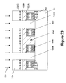
- FIGS. 23-24 depict yet another illustrative technique for forming storage node contacts in accordance with one illustrative aspect of the present invention.
- FIG. 3 depicts a portion of an illustrative memory cell 50 formed above a portion of a substrate 51 at an intermediate stage of manufacture for an illustrative DRAM device.
- the present invention is disclosed in the context of manufacturing an illustrative DRAM device. However, as those skilled in the art will recognize after a complete reading of the present application, the present invention is not limited to the manufacture of such devices, as other types of devices may be manufactured using the methods and techniques disclosed herein.
- the memory cell 50 comprises a plurality of isolation regions 54 , and an active area 52 .
- a plurality of access devices 53 (designated as 53 a and 53 b ), e.g., word lines, and a plurality of passing word lines 53 c .
- the access devices 53 may be “buried” type devices that are formed in the substrate 51 , or they may be more traditional unburied access devices that are formed above the surface of the substrate 51 .
- the access devices 53 are depicted as unburied access devices.
- the present invention may be employed with both buried and unburied access devices.
- the exact configuration of the access devices 53 may also vary and should not be considered a limitation of the present invention.
- the access devices 53 may comprise a gate insulating layer 57 a , a conductive layer 57 b , a metal silicide layer 57 c , a top insulating layer 57 d , such as, for example, a layer of silicon nitride, and a sidewall spacer 57 e.
- FIG. 3 also depicts a first insulating layer 56 formed above the substrate 51 .
- the first insulating layer 56 may be comprised of a variety of materials, e.g., silicon dioxide, BPSG, etc.
- the first layer of insulating material 56 may be formed by performing any of a variety of known deposition processes, e.g., chemical vapor deposition (CVD), plasma enhanced chemical vapor deposition (PECVD), etc.
- CVD chemical vapor deposition
- PECVD plasma enhanced chemical vapor deposition
- the first layer of insulating material 56 will be deposited such that its surface 58 extends above the surface 59 of the access devices 53 .
- CMP chemical mechanical polishing
- a hard mask layer 60 is deposited above the structure depicted in FIG. 3 .
- the hard mask layer 60 may be comprised of a variety of materials, and it may perform a variety of functions. As described more fully below, the hard mask layer 60 will ultimately be patterned and used as an etch mask in defining openings in the first insulating layer 56 for conductive contacts for the finished device.
- the hard mask layer 60 may also serve other purposes, e.g., it may act as an anti-reflective coating layer.
- the hard mask layer 60 may be referred to as a DARC (which may refer to a deposited anti-reflective coating or a dielectric anti-reflective coating).
- the hard mask layer 60 may be comprised of a variety of materials, other than photoresist materials, and it may be formed using a variety of techniques. Moreover, the thickness of the hard mask layer 60 may vary depending upon the particular application. In general, the hard mask layer 60 is comprised of a non-photoresist material that is selectively etchable with respect to the underlying insulating layer 56 . Illustrative materials for the hard mask layer 60 include, for example, silicon nitride, silicon oxynitride, carbon, etc. The hard mask layer 60 may be formed by, for example, performing a CVD process, and it may have any desired thickness, e.g., 700-2000 ⁇ . Thus, particular details of the illustrative hard mask layer 60 depicted herein should not be considered a limitation of the present invention.
- the hard mask layer 60 will be patterned by performing first and second partial etching processes using first and second masking layers 62 , 64 .
- the first and second masking layers 62 , 64 may be comprised of a variety of materials, e.g., photoresist. As will be recognized by those skilled in the art after reading the present application, the order in which the masking layers 62 , 64 and the associated etching processes are described herein may be reversed.
- the first patterned masking layer 62 is formed such that its features 62 a are parallel to and are positioned above the access devices 53 .
- a first etching process such as an anisotropic etching process, as indicated by the arrows 68 , is performed to partially etch the hard mask layer 60 , thereby defining recesses 66 , e.g., trenches, in the hard mask layer 60 .
- the etching process is controlled such that the trenches 66 formed during this first etching process do not extend through the partially etched hard mask layer 60 a .
- the first etching process may be performed such that the trenches 66 have a depth that equals approximately one-half of the starting thickness of the hard mask layer 60 .
- the second masking layer 64 may also be comprised of a variety of materials, e.g., a photoresist material.
- the second masking layer 64 is formed such that its features 64 a are substantially perpendicular to the features 62 a of the first masking layer 62 .
- the features 64 a of the second masking layer 64 are also substantially perpendicular to the access devices 53 , e.g., the word lines.
- the order and/or the orientation of the first and second masking layer 62 , 64 may be reversed.
- the partially etched hard mask layer 60 a will be subjected to a second partial etching process, e.g., an anisotropic etching process, as indicated by the arrows 71 .
- the second partial etching process 71 defines a plurality of trenches 69 (see FIG. 9 ) that are substantially perpendicular to the trenches 66 formed during the first partial etching process 68 (see FIG. 10 ).
- This second partial etching process like the first partial etching process, is designed such that it will not etch through the entire original thickness of the hard mask layer 60 .
- the portions of the hard mask layer 60 a that are exposed to both the first and second partial etching processes will be removed, thereby defining a plurality of generally rectangular shaped openings 70 (e.g., 70 a , 70 b , 70 c ), thereby exposing the underlying first layer of insulating material 56 .
- FIGS. 8 and 9 are, respectively, a perspective view and an end view depicting the patterned hard mask layer 60 b after it has been subjected to the first and second partial etching processes described above.
- FIG. 10 is a plan view showing the masking layer 60 b after it has been subjected to the two partial etching processes described above.
- FIG. 11 is a plan view of the patterned hard mask layer 60 b with the openings 70 a , 70 b and 70 c formed therein. For purposes of clarity, the associated trenches 66 , 69 are not depicted in FIG. 11 . Also note that an illustrative rectangular shaped active area 52 is depicted in dashed lines since it is positioned under the patterned hard mask layer 60 b .
- a plurality of openings 70 are formed in the patterned hard mask layer 60 b .
- the openings 70 are generally rectangular or square in shape due to the methodologies employed herein.
- precise geometric precision is not intended.
- precise geometric precision in the formation of such features is very difficult to achieve.
- a plurality of openings 70 u for adjacent memory cells are also partially shown in FIG. 10 .
- FIG. 12 is directed to an alternative embodiment wherein contact openings may be formed in the patterned hard mask layer 60 b for contacts to be formed within the memory array and for contacts formed outside of the memory array, e.g., in some of the peripheral circuitry.
- an opening 70 d for a contact to be formed outside of the array may be formed in the hard mask layer 60 b at the same time the openings for contacts within the array, e.g., openings 70 a , 70 b and 70 c , are formed in the hard mask layer 60 b .
- the opening 70 d is representative in nature in that it may represent a plurality of openings formed in the area outside of the array.
- the size of the openings 70 d and 70 a , 70 b and 70 c may vary depending on the particular application.
- a DRAM device is comprised of an array of memory cells 22 and a vast variety of peripheral circuitry, e.g., addressing circuitry 26 , sensing circuitry 24 , etc. Many of these peripheral circuits are formed in portions of the substrate at locations spaced apart from memory array 22 . These peripheral circuits also comprise active devices, e.g., transistors, capacitors, resistors, etc., that require the formation of conductive contacts. In prior art process flows, the formation of the conductive contacts to the peripheral circuits was done at a different point in time in the process flow relative to the formation of the conductive contacts within the memory array 22 .
- the present invention may result in less process steps, thereby improving manufacturing efficiency and reducing costs.
- the present invention may also remove various processing constraints, such as the SON CMP process discussed above.
- the present invention may enable the generation of additional process flows which may be more efficient.
- the patterned hard mask layer 60 b After the patterned hard mask layer 60 b is formed, it may be used as a mask in an etching process to form discrete contact openings in the memory array and in the regions outside of the memory array if desired. As shown in FIGS. 13 and 14 , the patterned hard mask layer 60 b with openings 70 a , 70 b and 70 c (without the array) and 70 d , 70 e and 70 f (outside of the array) formed therein is used as a mask in an etching process that is used to form contact openings 80 a , 80 b and 80 c (within the array) and 80 d , 80 e and 80 f (outside of the array).
- An illustrative device 81 e.g., a transistor, is depicted as part of a circuit located outside of the memory array that contains the memory cells.
- the present invention is not limited to use in situations where contact openings are formed both inside and outside of the memory array at the same time. That is, contact openings within the array and outside of the array may be formed at different times.
- a digitline contact will be formed in the opening 80 b
- storage node contacts will be formed in openings 80 a , 80 c
- contacts for the gate electrode and source/drain regions of the transistor 81 in the peripheral circuit will be formed in the openings 80 d , 80 e and 80 f .
- the precise methodology and techniques used to form the actual contacts may vary depending upon the application.
- the openings 80 a , 80 b , 80 c , 80 d , 80 e and 80 f will have the general shape as that of the openings 70 a , 70 b , 70 c , 70 d , 70 e and 70 f in the patterned hard mask layer 60 b , i.e., substantially rectangular or substantially square.
- the openings 80 a , 80 b , 80 c in the memory array, and openings 80 e and 80 f extend all the way to the active area 52 .
- the opening 80 d in the peripheral regions may extend all the way to the substrate 51 as well, or extend down to contact a device formed in the periphery region, such as a transistor, a resistor, a capacitor, etc.
- the openings in the insulating layer 56 may be filed with a conductive material, e.g., a metal, polysilicon, etc., using a variety of different process flows.
- a conductive material e.g., a metal, polysilicon, etc.
- any of a variety of different process flows may be employed to form conductive material in the openings 80 a , 80 b , 80 c , 80 d , 80 e and 80 f .
- a conductive material e.g., a metal, polysilicon, etc.
- a layer of conductive material 88 e.g., a metal such as tungsten, polysilicon, etc.
- a planarization process such as a chemical mechanical planarization process, is performed to remove excess portions of the conductive layer 88 that is positioned outside of the openings 80 a , 80 b , 80 c , 80 d , 80 e and 80 f .
- the contact 95 b is a digitline contact and the contacts 95 a and 95 c are storage node contacts for an illustrative dual bit memory cell 50 .
- the contact 95 d is a contact to the gate electrode of the transistor 81 and the contacts 95 e and 95 f contact the source/drain regions of the transistor 81 .
- FIGS. 17 and 18 depict another illustrative process flow for forming conductive contacts within the openings 80 a , 80 b , 80 c , 80 d , 80 e and 80 f .
- a conductive layer 90 e.g., tungsten
- a process layer 91 e.g., a layer of silicon nitride, is formed above the conductive layer 90 .
- a masking layer (not shown) comprised of a photoresist material is formed above the process layer 91 . Thereafter, one or more anisotropic etching processes are performed to essentially pattern the layers 90 and 91 , thereby resulting in the structure depicted in FIG. 18 . Note that the etching process may be performed until such time as the conductive layer 90 is recessed within the openings 80 a , 80 c , 80 d , 80 e and 80 f , thereby defining recessed contact members 96 a , 96 c , 96 d , 96 e and 96 f .
- the structure 96 b is a unitary or integral digitline contact structure that is contacted to the active area 52 .
- the contacts 96 a , 96 c are portions of storage node contacts for an illustrative dual bit memory cell.
- Subsequent processing steps may be performed to form contacts to the recessed contacts 96 a , 96 c , 96 d , 96 e and 96 f .
- contact may be made to the recessed contact members 96 a , 96 c , 96 d , 96 e and 96 f using the same or different conductive material.
- FIG. 19 depicts the device after the hard mask layer 60 b has been employed to define an opening 100 A for a digitline contact and two openings 100 B for storage node contacts.
- a bit line 102 is formed using traditional deposition techniques.
- the bit line 102 is comprised of a first layer of conductive material 102 A, e.g., tungsten, a second layer of conductive material 102 B, e.g., titanium, and a cap layer 102 C, e.g., silicon nitride.
- a variety of different materials may be employed to form the bit line 102 .
- a patterned masking layer 104 e.g., photoresist
- an etching process indicated by arrows 105 , is performed to define the digitline contact 106 and a first conductive portion 107 of the storage node contacts.
- the etching process 105 may be controlled to determine how much the first conductive portions 107 are recessed relative to the upper surface 99 of the word line structures 50 a , 50 b.
- the liner 108 may be formed from a variety of insulating materials, e.g., silicon dioxide, silicon nitride, etc.
- the liner 108 may be comprised of a low-k dielectric material, i.e., a material having a dielectric constant less than 7, i.e., less than the dielectric constant of silicon nitride.
- the liner 108 may be comprised of TEOS, silicon dioxide.
- the liner 108 may have a thickness ranging from 200-400 ⁇ and it may be formed using known conformal deposition techniques followed by an anisotropic etching process to clear the dielectric material from above the upper surface 107 A of the first conductive portion 107 . Thereafter, the second conductive portion 109 may be formed above the first conductive portion 107 . A conductive interface 115 is thereby established between the first conductive portion 107 and the second conductive portion 109 .
- the first and second conductive portions 107 , 109 may be formed of the same or different materials.
- the second conductive portion 109 may be formed by depositing a layer of conductive material, e.g., tungsten, titanium, etc., above the cap layer 102 C and in the openings between the liner 108 . A planarization process may then be performed to remove excess portions of the conductive material positioned above the cap layer 102 C to thereby define the second conductive portions 109 .
- a layer of conductive material e.g., tungsten, titanium, etc.
- FIGS. 23-24 depict an alternative process flow for an illustrative aspect of the present invention.
- the etching process 105 that is performed to form the digitline contact 106 is continued until such time as the entirety of the conductive material 102 A is cleared from the openings 100 B for the storage node contacts.
- the liner 108 is formed in the openings 100 B and a unitary conductive portion 110 is formed to constitute the storage node contact.
- the conductive portion 110 may be made of any conductive material, e.g., titanium, tungsten, etc., and it may be the same as or different from the material 102 A.
- the liner 108 extends along the entire length of the unitary conductive structure 110 , whereas, in the embodiment shown in FIG. 22 , the liner 108 extends along the entire length of the second conductive portion 109 .
- the present invention is generally directed to a method of forming contacts for a memory device.
- the method comprises forming a layer of insulating material above an active area of a dual bit memory cell, forming a hard mask layer above the layer of insulating material, the hard mask layer having an original thickness, performing at least two partial etching processes on the hard mask layer to thereby define a patterned hard mask layer above the layer of insulating material, wherein each of the partial etching processes is designed to etch through less than the original thickness of the hard mask layer, the hard mask layer having openings formed therein that correspond to a digitline contact and a plurality of storage node contacts for the dual bit memory cell, and performing at least one etching process to form openings in the layer of insulating material for the digitline contact and the plurality of storage node contacts using the patterned hard mask layer as an etch mask.
- the method comprises forming a layer of insulating material above an active area of a dual bit memory cell, forming a hard mask layer above the layer of insulating material, the hard mask layer having an original thickness, performing at least two partial etching processes on the hard mask layer to thereby define a patterned hard mask layer above the layer of insulating material, wherein each of the partial etching processes is designed to etch through less than the original thickness of the hard mask layer, the patterned hard mask layer being comprised of a material that is selectively etchable with respect to the layer of insulating material, the patterned hard mask layer having openings formed therein that correspond to a digitline contact and a plurality of storage node contacts for the dual bit memory cell, and performing a single etching process to form openings in the layer of insulating material for the digitline contact and the plurality of storage node contacts using the patterned hard mask layer as an etch mask.
- the method comprises forming a layer of insulating material above an active area of a dual bit memory cell, depositing a hard mask layer above the layer of insulating material, the hard mask layer having a deposited thickness, performing at least two partial etching processes on the deposited hard mask layer to form a patterned hard mask layer, wherein each of the partial etching processes is designed to etch through less than the entire deposited thickness of the hard mask layer, the hard mask layer having openings formed therein that correspond to a digitline contact and a plurality of storage node contacts for the dual bit memory cell, and performing at least one etching process to form openings in the layer of insulating material for the digitline contact and the plurality of storage node contacts using the patterned hard mask layer as an etch mask.
- the method comprises forming a layer of insulating material above an active area of a dual bit memory cell, forming a patterned hard mask layer above the layer of insulating material, the patterned hard mask layer being comprised of a material that is selectively etchable with respect to the layer of insulating material, the hard mask layer having openings formed therein that correspond to a digitline contact, a plurality of storage node contacts for the dual bit memory cell and an opening for a contact located in a peripheral circuit located outside of a memory array comprising the dual bit memory cell, and performing a single etching process to form openings in the layer of insulating material for the digitline contact, the plurality of storage node contacts and the contact for the peripheral circuit using the patterned hard mask layer as an etch mask.
Landscapes
- Engineering & Computer Science (AREA)
- Physics & Mathematics (AREA)
- Condensed Matter Physics & Semiconductors (AREA)
- General Physics & Mathematics (AREA)
- Computer Hardware Design (AREA)
- Microelectronics & Electronic Packaging (AREA)
- Power Engineering (AREA)
- Manufacturing & Machinery (AREA)
- Semiconductor Memories (AREA)
- Internal Circuitry In Semiconductor Integrated Circuit Devices (AREA)
Abstract
Description
Claims (36)
Priority Applications (4)
| Application Number | Priority Date | Filing Date | Title |
|---|---|---|---|
| US11/368,898 US7807582B2 (en) | 2006-03-06 | 2006-03-06 | Method of forming contacts for a memory device |
| US12/892,684 US8329534B2 (en) | 2006-03-06 | 2010-09-28 | Method of forming contacts for a memory device |
| US13/674,254 US9337053B2 (en) | 2006-03-06 | 2012-11-12 | Method of forming contacts for a memory device |
| US15/050,328 US10347638B2 (en) | 2006-03-06 | 2016-02-22 | Method of forming contacts for a memory device |
Applications Claiming Priority (1)
| Application Number | Priority Date | Filing Date | Title |
|---|---|---|---|
| US11/368,898 US7807582B2 (en) | 2006-03-06 | 2006-03-06 | Method of forming contacts for a memory device |
Related Child Applications (1)
| Application Number | Title | Priority Date | Filing Date |
|---|---|---|---|
| US12/892,684 Division US8329534B2 (en) | 2006-03-06 | 2010-09-28 | Method of forming contacts for a memory device |
Publications (2)
| Publication Number | Publication Date |
|---|---|
| US20070207620A1 US20070207620A1 (en) | 2007-09-06 |
| US7807582B2 true US7807582B2 (en) | 2010-10-05 |
Family
ID=38471972
Family Applications (4)
| Application Number | Title | Priority Date | Filing Date |
|---|---|---|---|
| US11/368,898 Active 2028-11-30 US7807582B2 (en) | 2006-03-06 | 2006-03-06 | Method of forming contacts for a memory device |
| US12/892,684 Active 2026-11-15 US8329534B2 (en) | 2006-03-06 | 2010-09-28 | Method of forming contacts for a memory device |
| US13/674,254 Active 2026-09-05 US9337053B2 (en) | 2006-03-06 | 2012-11-12 | Method of forming contacts for a memory device |
| US15/050,328 Active 2027-02-20 US10347638B2 (en) | 2006-03-06 | 2016-02-22 | Method of forming contacts for a memory device |
Family Applications After (3)
| Application Number | Title | Priority Date | Filing Date |
|---|---|---|---|
| US12/892,684 Active 2026-11-15 US8329534B2 (en) | 2006-03-06 | 2010-09-28 | Method of forming contacts for a memory device |
| US13/674,254 Active 2026-09-05 US9337053B2 (en) | 2006-03-06 | 2012-11-12 | Method of forming contacts for a memory device |
| US15/050,328 Active 2027-02-20 US10347638B2 (en) | 2006-03-06 | 2016-02-22 | Method of forming contacts for a memory device |
Country Status (1)
| Country | Link |
|---|---|
| US (4) | US7807582B2 (en) |
Cited By (2)
| Publication number | Priority date | Publication date | Assignee | Title |
|---|---|---|---|---|
| US20130149862A1 (en) * | 2009-12-28 | 2013-06-13 | Samsung Electronics Co., Ltd. | Method for forming fine pattern having variable width and method for manufacturing semiconductor device using the same |
| US9287161B2 (en) | 2013-11-21 | 2016-03-15 | Samsung Electronics Co., Ltd. | Method of forming wirings |
Families Citing this family (13)
| Publication number | Priority date | Publication date | Assignee | Title |
|---|---|---|---|---|
| US7807582B2 (en) * | 2006-03-06 | 2010-10-05 | Micron Technology, Inc. | Method of forming contacts for a memory device |
| US8030215B1 (en) | 2008-02-19 | 2011-10-04 | Marvell International Ltd. | Method for creating ultra-high-density holes and metallization |
| KR101658492B1 (en) * | 2010-08-13 | 2016-09-21 | 삼성전자주식회사 | Method for forming fine patterns and method for manufacturing a semiconductor device by using the same |
| KR101671464B1 (en) | 2010-12-02 | 2016-11-02 | 삼성전자주식회사 | Method for manufacturing a semiconductor device |
| KR101926418B1 (en) * | 2012-05-16 | 2018-12-10 | 삼성전자주식회사 | method for manufacturing a semiconductor device |
| US9786597B2 (en) * | 2013-03-11 | 2017-10-10 | International Business Machines Corporation | Self-aligned pitch split for unidirectional metal wiring |
| KR20160074826A (en) | 2014-12-18 | 2016-06-29 | 삼성전자주식회사 | Semiconductor device |
| CN108269758B (en) | 2016-12-29 | 2019-08-23 | 联华电子股份有限公司 | The production method of semiconductor element |
| CN108573926B (en) * | 2017-03-09 | 2020-01-21 | 联华电子股份有限公司 | Semiconductor memory device and method of manufacturing the same |
| US11158571B2 (en) | 2018-12-20 | 2021-10-26 | Micron Technology, Inc. | Devices including conductive interconnect structures, related electronic systems, and related methods |
| US11430793B2 (en) | 2020-06-11 | 2022-08-30 | Micron Technology, Inc. | Microelectronic devices including passing word line structures, and related electronic systems and methods |
| US11569353B2 (en) | 2021-02-02 | 2023-01-31 | Micron Technology, Inc. | Apparatuses including passing word lines comprising a band offset material, and related methods and systems |
| TWI820996B (en) * | 2022-11-02 | 2023-11-01 | 華邦電子股份有限公司 | Semiconductor structure and manufacturing method thereof |
Citations (7)
| Publication number | Priority date | Publication date | Assignee | Title |
|---|---|---|---|---|
| US6218089B1 (en) | 1998-05-22 | 2001-04-17 | Micron Technology, Inc. | Photolithographic method |
| US6429474B1 (en) * | 1999-04-28 | 2002-08-06 | International Business Machines Corporation | Storage-capacitor electrode and interconnect |
| US6548347B2 (en) | 2001-04-12 | 2003-04-15 | Micron Technology, Inc. | Method of forming minimally spaced word lines |
| US6777260B1 (en) * | 2003-08-14 | 2004-08-17 | Silicon Storage Technology, Inc. | Method of making sub-lithographic sized contact holes |
| US20050186802A1 (en) | 2004-02-20 | 2005-08-25 | Busch Brett W. | Methods of Forming Openings, And Methods of Forming Container Capacitors |
| US20050277276A1 (en) * | 2004-05-25 | 2005-12-15 | Stephens Tab A | Decoupled complementary mask patterning transfer method |
| US20060189063A1 (en) * | 2003-07-12 | 2006-08-24 | Koninklijke Philips Electronics N.V. | Insulated gate power semiconductor devices |
Family Cites Families (6)
| Publication number | Priority date | Publication date | Assignee | Title |
|---|---|---|---|---|
| US5066606A (en) * | 1990-12-07 | 1991-11-19 | Micron Technology, Inc. | Implant method for advanced stacked capacitors |
| US6844694B2 (en) | 2001-08-10 | 2005-01-18 | Nikon Corporation | Stage assembly and exposure apparatus including the same |
| KR100632938B1 (en) * | 2004-12-22 | 2006-10-12 | 삼성전자주식회사 | DRAM device having capacitor and method of forming the same |
| US7807582B2 (en) * | 2006-03-06 | 2010-10-05 | Micron Technology, Inc. | Method of forming contacts for a memory device |
| US7560392B2 (en) * | 2006-05-10 | 2009-07-14 | Micron Technology, Inc. | Electrical components for microelectronic devices and methods of forming the same |
| WO2009031052A2 (en) * | 2007-03-29 | 2009-03-12 | Innovative Silicon S.A. | Zero-capacitor (floating body) random access memory circuits with polycide word lines and manufacturing methods therefor |
-
2006
- 2006-03-06 US US11/368,898 patent/US7807582B2/en active Active
-
2010
- 2010-09-28 US US12/892,684 patent/US8329534B2/en active Active
-
2012
- 2012-11-12 US US13/674,254 patent/US9337053B2/en active Active
-
2016
- 2016-02-22 US US15/050,328 patent/US10347638B2/en active Active
Patent Citations (9)
| Publication number | Priority date | Publication date | Assignee | Title |
|---|---|---|---|---|
| US6218089B1 (en) | 1998-05-22 | 2001-04-17 | Micron Technology, Inc. | Photolithographic method |
| US6429474B1 (en) * | 1999-04-28 | 2002-08-06 | International Business Machines Corporation | Storage-capacitor electrode and interconnect |
| US6548347B2 (en) | 2001-04-12 | 2003-04-15 | Micron Technology, Inc. | Method of forming minimally spaced word lines |
| US6627933B2 (en) | 2001-04-12 | 2003-09-30 | Micron Technology, Inc. | Method of forming minimally spaced word lines |
| US6844594B2 (en) | 2001-04-12 | 2005-01-18 | Micron Technology, Inc. | Minimally spaced gates and word lines |
| US20060189063A1 (en) * | 2003-07-12 | 2006-08-24 | Koninklijke Philips Electronics N.V. | Insulated gate power semiconductor devices |
| US6777260B1 (en) * | 2003-08-14 | 2004-08-17 | Silicon Storage Technology, Inc. | Method of making sub-lithographic sized contact holes |
| US20050186802A1 (en) | 2004-02-20 | 2005-08-25 | Busch Brett W. | Methods of Forming Openings, And Methods of Forming Container Capacitors |
| US20050277276A1 (en) * | 2004-05-25 | 2005-12-15 | Stephens Tab A | Decoupled complementary mask patterning transfer method |
Cited By (3)
| Publication number | Priority date | Publication date | Assignee | Title |
|---|---|---|---|---|
| US20130149862A1 (en) * | 2009-12-28 | 2013-06-13 | Samsung Electronics Co., Ltd. | Method for forming fine pattern having variable width and method for manufacturing semiconductor device using the same |
| US8598036B2 (en) * | 2009-12-28 | 2013-12-03 | Samsung Electronics Co., Ltd. | Method for forming fine pattern having variable width and method for manufacturing semiconductor device using the same |
| US9287161B2 (en) | 2013-11-21 | 2016-03-15 | Samsung Electronics Co., Ltd. | Method of forming wirings |
Also Published As
| Publication number | Publication date |
|---|---|
| US20160172363A1 (en) | 2016-06-16 |
| US10347638B2 (en) | 2019-07-09 |
| US8329534B2 (en) | 2012-12-11 |
| US20130069220A1 (en) | 2013-03-21 |
| US9337053B2 (en) | 2016-05-10 |
| US20110014787A1 (en) | 2011-01-20 |
| US20070207620A1 (en) | 2007-09-06 |
Similar Documents
| Publication | Publication Date | Title |
|---|---|---|
| US10347638B2 (en) | Method of forming contacts for a memory device | |
| TWI471981B (en) | Method for fabricating memory device with buried digit lines and buried word lines | |
| TWI615921B (en) | Semiconductor memory device having coplanar digit line contacts and storage node contacts in memory array and method for fabricating the same | |
| US6905944B2 (en) | Sacrificial collar method for improved deep trench processing | |
| US5956587A (en) | Method for crown type capacitor in dynamic random access memory | |
| US6710391B2 (en) | Integrated DRAM process/structure using contact pillars | |
| US7595262B2 (en) | Manufacturing method for an integrated semiconductor structure | |
| US20010055221A1 (en) | Method for forming gate segments for an integrated circuit | |
| US6503796B1 (en) | Method and structure for a top plate design for making capacitor-top-plate to bit-line-contact overlay margin | |
| US6548850B1 (en) | Trench capacitor configuration and method of producing it | |
| JP2005019988A (en) | Semiconductor device and manufacturing method therefor | |
| US5837581A (en) | Method for forming a capacitor using a hemispherical-grain structure | |
| US5536673A (en) | Method for making dynamic random access memory (DRAM) cells having large capacitor electrode plates for increased capacitance | |
| US8748961B2 (en) | Buried bit line process and scheme | |
| US6821872B1 (en) | Method of making a bit line contact device | |
| US6909136B2 (en) | Trench-capacitor DRAM cell having a folded gate conductor | |
| US6653230B2 (en) | Semiconductor device having concave electrode and convex electrode and method of manufacturing thereof | |
| US6153465A (en) | Method of fabricating a capacitor of dynamic random access memory | |
| US5759893A (en) | Method of fabricating a rugged-crown shaped capacitor | |
| KR20100110098A (en) | Method for manufacturing semiconductor device | |
| US6753252B2 (en) | Contact plug formation for devices with stacked capacitors | |
| US6090663A (en) | Method for forming a high-density DRAM cell with a rugged polysilicon cup-shaped capacitor | |
| US7078290B2 (en) | Method for forming a top oxide with nitride liner | |
| US20020064956A1 (en) | Method of forming a storage node of a capacitor | |
| US6091098A (en) | Double-crown rugged polysilicon capacitor |
Legal Events
| Date | Code | Title | Description |
|---|---|---|---|
| AS | Assignment |
Owner name: MICRON TECHNOLOGY, INC., IDAHO Free format text: ASSIGNMENT OF ASSIGNORS INTEREST;ASSIGNOR:DOEBLER, JONATHAN;REEL/FRAME:017654/0263 Effective date: 20060302 |
|
| FEPP | Fee payment procedure |
Free format text: PAYOR NUMBER ASSIGNED (ORIGINAL EVENT CODE: ASPN); ENTITY STATUS OF PATENT OWNER: LARGE ENTITY |
|
| STCF | Information on status: patent grant |
Free format text: PATENTED CASE |
|
| CC | Certificate of correction | ||
| FPAY | Fee payment |
Year of fee payment: 4 |
|
| AS | Assignment |
Owner name: U.S. BANK NATIONAL ASSOCIATION, AS COLLATERAL AGENT, CALIFORNIA Free format text: SECURITY INTEREST;ASSIGNOR:MICRON TECHNOLOGY, INC.;REEL/FRAME:038669/0001 Effective date: 20160426 Owner name: U.S. BANK NATIONAL ASSOCIATION, AS COLLATERAL AGEN Free format text: SECURITY INTEREST;ASSIGNOR:MICRON TECHNOLOGY, INC.;REEL/FRAME:038669/0001 Effective date: 20160426 |
|
| AS | Assignment |
Owner name: MORGAN STANLEY SENIOR FUNDING, INC., AS COLLATERAL AGENT, MARYLAND Free format text: PATENT SECURITY AGREEMENT;ASSIGNOR:MICRON TECHNOLOGY, INC.;REEL/FRAME:038954/0001 Effective date: 20160426 Owner name: MORGAN STANLEY SENIOR FUNDING, INC., AS COLLATERAL Free format text: PATENT SECURITY AGREEMENT;ASSIGNOR:MICRON TECHNOLOGY, INC.;REEL/FRAME:038954/0001 Effective date: 20160426 |
|
| AS | Assignment |
Owner name: U.S. BANK NATIONAL ASSOCIATION, AS COLLATERAL AGENT, CALIFORNIA Free format text: CORRECTIVE ASSIGNMENT TO CORRECT THE REPLACE ERRONEOUSLY FILED PATENT #7358718 WITH THE CORRECT PATENT #7358178 PREVIOUSLY RECORDED ON REEL 038669 FRAME 0001. ASSIGNOR(S) HEREBY CONFIRMS THE SECURITY INTEREST;ASSIGNOR:MICRON TECHNOLOGY, INC.;REEL/FRAME:043079/0001 Effective date: 20160426 Owner name: U.S. BANK NATIONAL ASSOCIATION, AS COLLATERAL AGEN Free format text: CORRECTIVE ASSIGNMENT TO CORRECT THE REPLACE ERRONEOUSLY FILED PATENT #7358718 WITH THE CORRECT PATENT #7358178 PREVIOUSLY RECORDED ON REEL 038669 FRAME 0001. ASSIGNOR(S) HEREBY CONFIRMS THE SECURITY INTEREST;ASSIGNOR:MICRON TECHNOLOGY, INC.;REEL/FRAME:043079/0001 Effective date: 20160426 |
|
| MAFP | Maintenance fee payment |
Free format text: PAYMENT OF MAINTENANCE FEE, 8TH YEAR, LARGE ENTITY (ORIGINAL EVENT CODE: M1552) Year of fee payment: 8 |
|
| AS | Assignment |
Owner name: JPMORGAN CHASE BANK, N.A., AS COLLATERAL AGENT, ILLINOIS Free format text: SECURITY INTEREST;ASSIGNORS:MICRON TECHNOLOGY, INC.;MICRON SEMICONDUCTOR PRODUCTS, INC.;REEL/FRAME:047540/0001 Effective date: 20180703 Owner name: JPMORGAN CHASE BANK, N.A., AS COLLATERAL AGENT, IL Free format text: SECURITY INTEREST;ASSIGNORS:MICRON TECHNOLOGY, INC.;MICRON SEMICONDUCTOR PRODUCTS, INC.;REEL/FRAME:047540/0001 Effective date: 20180703 |
|
| AS | Assignment |
Owner name: MICRON TECHNOLOGY, INC., IDAHO Free format text: RELEASE BY SECURED PARTY;ASSIGNOR:U.S. BANK NATIONAL ASSOCIATION, AS COLLATERAL AGENT;REEL/FRAME:047243/0001 Effective date: 20180629 |
|
| AS | Assignment |
Owner name: MICRON TECHNOLOGY, INC., IDAHO Free format text: RELEASE BY SECURED PARTY;ASSIGNOR:MORGAN STANLEY SENIOR FUNDING, INC., AS COLLATERAL AGENT;REEL/FRAME:050937/0001 Effective date: 20190731 |
|
| AS | Assignment |
Owner name: MICRON SEMICONDUCTOR PRODUCTS, INC., IDAHO Free format text: RELEASE BY SECURED PARTY;ASSIGNOR:JPMORGAN CHASE BANK, N.A., AS COLLATERAL AGENT;REEL/FRAME:051028/0001 Effective date: 20190731 Owner name: MICRON TECHNOLOGY, INC., IDAHO Free format text: RELEASE BY SECURED PARTY;ASSIGNOR:JPMORGAN CHASE BANK, N.A., AS COLLATERAL AGENT;REEL/FRAME:051028/0001 Effective date: 20190731 |
|
| MAFP | Maintenance fee payment |
Free format text: PAYMENT OF MAINTENANCE FEE, 12TH YEAR, LARGE ENTITY (ORIGINAL EVENT CODE: M1553); ENTITY STATUS OF PATENT OWNER: LARGE ENTITY Year of fee payment: 12 |