US7797608B2 - Decoding device in optical disc drive and related decoding method thereof - Google Patents

Decoding device in optical disc drive and related decoding method thereof Download PDF

Info

Publication number
US7797608B2
US7797608B2 US11/558,927 US55892706A US7797608B2 US 7797608 B2 US7797608 B2 US 7797608B2 US 55892706 A US55892706 A US 55892706A US 7797608 B2 US7797608 B2 US 7797608B2
Authority
US
United States
Prior art keywords
data
buffer
error
decoding
rewriting
Prior art date
Legal status (The legal status is an assumption and is not a legal conclusion. Google has not performed a legal analysis and makes no representation as to the accuracy of the status listed.)
Active, expires
Application number
US11/558,927
Other versions
US20070118789A1 (en
Inventor
Hui-Huang Chang
Chien-Chih Chen
Current Assignee (The listed assignees may be inaccurate. Google has not performed a legal analysis and makes no representation or warranty as to the accuracy of the list.)
Realtek Semiconductor Corp
Original Assignee
Realtek Semiconductor Corp
Priority date (The priority date is an assumption and is not a legal conclusion. Google has not performed a legal analysis and makes no representation as to the accuracy of the date listed.)
Filing date
Publication date
Application filed by Realtek Semiconductor Corp filed Critical Realtek Semiconductor Corp
Assigned to REALTEK SEMICONDUCTOR CORP. reassignment REALTEK SEMICONDUCTOR CORP. ASSIGNMENT OF ASSIGNORS INTEREST (SEE DOCUMENT FOR DETAILS). Assignors: CHANG, HUI-HUANG, CHEN, CHIEN-CHIH
Publication of US20070118789A1 publication Critical patent/US20070118789A1/en
Application granted granted Critical
Publication of US7797608B2 publication Critical patent/US7797608B2/en
Active legal-status Critical Current
Adjusted expiration legal-status Critical

Links

Images

Classifications

    • GPHYSICS
    • G11INFORMATION STORAGE
    • G11BINFORMATION STORAGE BASED ON RELATIVE MOVEMENT BETWEEN RECORD CARRIER AND TRANSDUCER
    • G11B20/00Signal processing not specific to the method of recording or reproducing; Circuits therefor
    • G11B20/10Digital recording or reproducing
    • G11B20/18Error detection or correction; Testing, e.g. of drop-outs
    • G11B20/1833Error detection or correction; Testing, e.g. of drop-outs by adding special lists or symbols to the coded information
    • GPHYSICS
    • G06COMPUTING; CALCULATING OR COUNTING
    • G06FELECTRIC DIGITAL DATA PROCESSING
    • G06F11/00Error detection; Error correction; Monitoring
    • G06F11/07Responding to the occurrence of a fault, e.g. fault tolerance
    • G06F11/08Error detection or correction by redundancy in data representation, e.g. by using checking codes
    • G06F11/10Adding special bits or symbols to the coded information, e.g. parity check, casting out 9's or 11's
    • GPHYSICS
    • G11INFORMATION STORAGE
    • G11BINFORMATION STORAGE BASED ON RELATIVE MOVEMENT BETWEEN RECORD CARRIER AND TRANSDUCER
    • G11B20/00Signal processing not specific to the method of recording or reproducing; Circuits therefor
    • G11B20/10Digital recording or reproducing
    • G11B20/10527Audio or video recording; Data buffering arrangements
    • G11B2020/1062Data buffering arrangements, e.g. recording or playback buffers
    • G11B2020/1075Data buffering arrangements, e.g. recording or playback buffers the usage of the buffer being restricted to a specific kind of data
    • G11B2020/10759Data buffering arrangements, e.g. recording or playback buffers the usage of the buffer being restricted to a specific kind of data content data
    • GPHYSICS
    • G11INFORMATION STORAGE
    • G11BINFORMATION STORAGE BASED ON RELATIVE MOVEMENT BETWEEN RECORD CARRIER AND TRANSDUCER
    • G11B20/00Signal processing not specific to the method of recording or reproducing; Circuits therefor
    • G11B20/10Digital recording or reproducing
    • G11B20/18Error detection or correction; Testing, e.g. of drop-outs
    • G11B20/1816Testing
    • G11B2020/1823Testing wherein a flag is set when errors are detected or qualified
    • GPHYSICS
    • G11INFORMATION STORAGE
    • G11BINFORMATION STORAGE BASED ON RELATIVE MOVEMENT BETWEEN RECORD CARRIER AND TRANSDUCER
    • G11B20/00Signal processing not specific to the method of recording or reproducing; Circuits therefor
    • G11B20/10Digital recording or reproducing
    • G11B20/18Error detection or correction; Testing, e.g. of drop-outs
    • G11B20/1833Error detection or correction; Testing, e.g. of drop-outs by adding special lists or symbols to the coded information
    • G11B2020/1853Error detection or correction; Testing, e.g. of drop-outs by adding special lists or symbols to the coded information using a product code which has inner and outer parity symbols

Definitions

  • This invention relates to an apparatus and a method for data decoding, and more particularly, to a decoding device applied in an optical disc drive and a related decoding method thereof.
  • FIG. 1 is a block diagram of the conventional DVD playback system 100 .
  • the DVD playback system 100 includes an EFM+ demodulator 110 , a main data storage device 120 , a decoding device 130 , a decoding result confirmation unit 140 , an ATAPI interface unit 150 , and a bus 160 .
  • the decoding device 130 includes an inner-code parity (PI) syndrome generator 132 , a PI error correction unit 134 , an outer-code parity (PO) syndrome generator 136 , a PO error correction unit 138 , and a decoding unit 139 .
  • PI inner-code parity
  • PO outer-code parity
  • the data will be demodulated by the EFM+ demodulator unit 110 and then stored in the main data storage device 120 .
  • the PI syndrome generator 132 reads the data progressively from the main storage device 120 through the bus 160 according to the PI direction (i.e. the horizontal direction) and then generates the PI syndrome.
  • the decoding unit 139 e.g. the Reed Solomon Product Code (RSPC) decoder
  • RSPC Reed Solomon Product Code
  • the PI error correction unit 134 then executes the data error correction process to the data by the PI direction, and restores the corrected data into the main storage device 120 through the bus 160 .
  • the PO syndrome generator 136 reads the data discontinuously from the main storage device 120 through the bus 160 according to the PO direction (i.e. the vertical direction) and then generates the PO syndrome. Accordingly, the decoding unit 139 executes the outer-code parity decoding process to the data according to the PO syndrome. According to the decoding result, the PO error address and PO error value generated by the decoding unit 139 are sent to the PO error correction unit 138 .
  • the PO error correction unit 138 then executes the data error correction process to the data by the PO direction and restores the corrected data into the main storage device 120 through the bus 160 .
  • the decoding result confirmation unit 140 (e.g. a descramble and EDC check unit) thus reads data from the main data storage device 120 to check whether the error-correction procedure is completed. If the decoding result confirmation unit 140 determines that the data stored in the main data storage device 120 is correct, the conventional DVD playback system 100 will transfer the data from the main data storage device 120 to a host by means of the ATAPI interface unit 150 .
  • a decoding device is disclosed.
  • the decoding device is utilized for processing an uncorrected data in a data storage medium.
  • the uncorrected data comprises a first direction error data and a second direction error data.
  • the decoding device comprises: an error correction unit receiving the uncorrected data, for correcting the second direction error data of the uncorrected data according to a second direction decoding information and outputting a data; a data buffer, coupled to the error correction unit, for buffering the data and outputting a corrected data after the first direction error data of the data is corrected; a first decoding unit, coupled to the data buffer, for decoding and correcting the first direction error data of the data stored in the data buffer; and a second decoding unit, coupled to the data buffer and the error correction unit, for generating the second direction decoding information to the error correction unit according to the data stored in the data buffer.
  • FIG. 1 is a block diagram of the conventional DVD playback system.
  • FIG. 2 is a block diagram of the DVD playback system having a decoding device according to the first embodiment of the present invention.
  • FIG. 3 shows a flowchart illustrating the data decoding and error correction operation of the decoding device shown in FIG. 2 .
  • FIG. 4 is a block diagram of the DVD playback system having a decoding device according to the second embodiment of the present invention.
  • FIG. 5 is a block diagram of the DVD playback system having a decoding device according to the third embodiment of the present invention.
  • FIG. 6 is a block diagram of the DVD playback system having a decoding device according to the fourth embodiment of the present invention.
  • FIG. 7 is a block diagram of the first embodiment of the rewriting unit shown in FIG. 6 .
  • FIG. 8 is a block diagram of the second embodiment of the rewriting unit shown in FIG. 6 .
  • FIG. 9 is a block diagram of the DVD playback system having a decoding device according to the fifth embodiment of the present invention.
  • FIG. 10 is a block diagram of the DVD playback system having a decoding device according to the sixth embodiment of the present invention.
  • FIG. 2 is a block diagram of the DVD playback system 200 including a decoding device 230 according to the first embodiment of the present invention.
  • the playback system 200 includes an EFM+ demodulator 210 , a main data storage device 220 (e.g. Dynamic Random Access Memory), a decoding device 230 , a decoding result confirmation unit 240 , an ATAPI interface unit 250 , and a bus 260 .
  • the decoding device 230 includes an error correction unit 231 , a data buffer 234 , a PI decoding unit 236 , and a PO decoding unit 237 .
  • the error correction unit 231 includes a PO error information register 233 and a dynamic correction unit 232 .
  • the decoding device 230 reads the data from the main data storage device 220 to the error correction unit 231 . Since this is the first time to read the data, the error information register 233 does not have any PO-relative error information and error address. The data will therefore be directly sent to the data buffer 234 .
  • the decoding device 230 reads the data progressively from the main data storage device 220 according to the PI direction. The data read by the decoding device 230 is continuous data; the main storage device 220 thus avoids the additional burden of discontinuous data reading.
  • the PI decoding unit 236 decodes and corrects the data stored in the data buffer 234 in sequence according to the PI direction, and generates the PI direction error value and error address.
  • the PI direction error value and error address are then utilized to process a logic calculation (normally an XOR calculation) with the data corresponding to the error address.
  • the correct data generated from the calculation is rewritten into the data buffer 234 to finish the operation of the PI direction error correction.
  • the PI corrected data is then written into the main data storage device 220 .
  • the PO decoding unit 237 decodes the data stored in the data buffer 234 according to the PO direction to generate the PO direction error value and error address, and then sends the PO direction error value and error address to the PO error information register 233 of the error correction unit 231 .
  • the decoding device 230 reads the data in sequence according to the PI direction from the main data storage device 220 , and sends the data into the error correction unit 231 .
  • the dynamic correction unit 232 is able to correct the data according to the PO direction and write the corrected data into the main data storage device 220 .
  • the decoding result confirmation unit 240 reads data from the main data storage device 220 and checks if the operation of error correction is completed. Finally the ATAPI interface unit 250 sends the corrected data from the main data storage device 220 to a host in order to execute the following data processing schedule.
  • the data buffer 234 is utilized for registering and buffering the data from the error correction unit 231 and for PI direction decoding and PO direction decoding. With the assistance of the error correction unit 231 , the data stored in the data buffer 234 can finally be rewritten in sequence into the main data storage device 220 . Please note that, in this moment; the data buffer 234 writes the whole data (including the error corrected data, the data with indeterminable errors, and the originally correct data) into the main data storage device 220 in sequence.
  • the decoding device 230 in the present invention does not need to write the corrected data randomly into the main storage device 220 as in the related art. Therefore the decoding device 230 in the present invention reduces the bandwidth and access time of the main data storage device 220 and increases the data access efficiency of the main data storage device 220 .
  • FIG. 3 shows a flowchart illustrating the data decoding and error correction operation of the decoding device 230 shown in FIG. 2 .
  • Related steps shown in the flow chart do not necessarily need to be sequentially executed; other steps may be inserted between the present steps. In general, however, the results are the same.
  • the processes of data decoding and error correction are detailed in the following:
  • Step 300 Start.
  • Step 302 The decoding device 230 reads a plurality of un-decoded data from the main data storage device 220 in sequence according to the PI direction, and stores each un-decoded data progressively into the data buffer 234 .
  • Step 304 The PI decoding unit 236 decodes the data stored in the data buffer 234 in sequence according to the PI direction, utilizes the decoded PI direction error value and error address to process a logic calculation (normally an XOR calculation) with the data corresponding to the error address, and rewrites the calculated data into the data buffer 234 to finish the PI direction error correction process.
  • a logic calculation normally an XOR calculation
  • Step 306 The PO decoding unit 237 decodes the data stored in the data buffer 234 according to the PO direction, generates the PO direction error value and error address and registers the PO direction error value and error address to the PO error information register 233 .
  • Step 308 The data buffer 234 writes its registered data in sequence back into the main data storage device 220 according to the PI direction.
  • Step 310 The decoding device 240 determines whether the data correction is completed and correct by checking the data stored in the data storage device 220 . If the correction is completed, the process goes to step 312 .
  • Step 312 The decoding device 230 reads a plurality of un-decoded data from the main data storage device 220 in sequence according to the PI direction.
  • Step 314 The dynamic correction unit 232 processes each un-decoded data progressively, corrects the error portion of each un-decoded data according to the error value and error address stored in the PO error information register 233 , and then writes the processed un-decoded data into the data buffer 234 .
  • Step 316 The PI decoding unit 236 decodes the data stored in the data buffer 234 in sequence according to the PI direction, utilizes the decoded PI direction error value and error address to process a logic calculation (normally an XOR calculation) with the data corresponding to the error address, and rewrites the calculated data into the data buffer 234 to finish the PI direction error correction process.
  • a logic calculation normally an XOR calculation
  • Step 318 The PO decoding unit 237 decodes the data stored in the data buffer 234 according to the PO direction, generates the PO direction error value and error address, and registers the PO direction error value and error address to the PO error information register 233 .
  • Step 320 The data buffer 234 writes the stored data into the main data storage device 220 in sequence according to the PI direction, and then goes back to step 310 .
  • Step 322 End.
  • FIG. 4 is a block diagram of the DVD playback system 400 including a decoding device 430 according to the second embodiment of the present invention
  • FIG. 5 is a block diagram of the DVD playback system 500 including a decoding device 530 according to the third embodiment of the present invention.
  • FIG. 4 and FIG. 5 have the same function and operation, detailed description is omitted for the sake of brevity.
  • the PI decoding unit 436 of the decoding device 430 directly receives each un-decoded data from the main data storage device 220 , and processes the operation of decoding and correcting the data according to the PI direction and error correction. After decoding and correcting, the corrected data will be sent into the data buffer 234 .
  • the DVD playback system 400 therefore reduces the data access frequency and lowers the bandwidth requirement for the data buffer 234 .
  • the difference between the DVD playback system 500 shown in FIG. 5 and the DVD playback system 400 shown in FIG. 4 is that the decoding result confirmation unit 540 is directly coupled to the data buffer 234 .
  • the decoding result confirmation unit 540 is able to receive the data stored in the data buffer 234 simultaneously and to determine whether the error correction process is completed. In other words, the decoding result confirmation unit 540 does not need to read the data rewritten by the data buffer 234 from the main data storage device 220 through the bus 260 . Accordingly, the DVD playback system can greatly reduce the data access frequency, as well as the bandwidth consumption, of the main data storage device 220 .
  • the data buffer 234 writes the whole stored data (including the error corrected data, the data with indeterminable error, and the originally correct data) into the main data storage device 220 in sequence. If only a few data have errors (i.e. most of the data in the main data storage device 220 are correct), only the corrected data need to be rewritten into the main data storage device 220 in order to reduce the required memory bandwidth. In this situation, the present invention further provides a data rewritten mechanism to determine whether to write the whole data in sequence or to only write the corrected data back to the main data storage device 220 according to different data error quantities.
  • FIG. 6 is a block diagram of the DVD playback system 600 including a decoding device 630 according to the fourth embodiment of the present invention. Please note that, since the same name elements of the DVD playback system 200 and 600 shown in FIG. 2 and FIG. 6 have the same function and operation, detailed description is omitted for the sake of brevity.
  • the DVD playback system 600 additionally sets a correction flag buffer 610 and a rewriting unit 620 .
  • the PI decoding unit 236 When the PI decoding unit 236 processes the operation of the PI direction error correction to the data inputted into the decoding device 630 , the PI decoding unit 236 sets an error correction flag stored in the correction flag buffer 610 according to the location of the corrected data. That is, when the dynamic correction unit 232 processes the error correction operation to the data inputted into the decoding device 630 , the dynamic correction unit 232 also sets an error correction flag stored in the correction flag buffer 610 according to the location of the corrected data. In other words, the error correction flag is utilized for indicating a data section stored in the data buffer 234 that has been error corrected.
  • each error correction flag (1 bit) can mark the data with one byte to recognize if the data is error corrected.
  • the correction flag buffer 610 stores 128 error correction flags. That is, when the number “n” byte of the data is error corrected, the number “n” error correction flag of the 128 error correction flags then will be marked as a first flag value (e.g. the logical value “1”).
  • the number n+1 error correction flag of the 128 error correction flags will therefore be marked with another flag value (e.g. the logical value “0”).
  • the length of each data section corresponding to the error correction flag can be determined according to the hardware structure of the main data storage device 220 .
  • the main data storage device can access 32 bits (4 bytes) in each clock cycle, and therefore one error correction flag (1 bit) can mark the data with 4 bytes to recognize if the data is error corrected.
  • the rewriting unit 620 can determine the data rewriting mechanism according to the error correction flag recorded in the correction flag buffer 610 .
  • the rewriting unit 620 can write the whole data stored in the data buffer 234 back to the main data storage device 220 according to the rewriting mechanism of the above embodiments. If the quantity of error data is less than the threshold value, however, the rewriting unit 620 can, as in the conventional method, randomly write the data section, which is error corrected and stored in the data buffer 234 , back to the main data storage device 220 according to the error correction flag in the correction flag buffer 610 .
  • FIG. 7 is a block diagram of the first embodiment of the rewriting unit 620 shown in FIG. 6 .
  • the rewriting unit 620 includes a rewriting buffer 622 , a counter 624 , and a switch module 626 .
  • the rewriting buffer 622 is utilized to store the data section (at least including the corrected data) and the related address information, which is ready to be rewritten to the main data storage device 220 .
  • the switch module 626 determines whether to couple the data buffer 234 and the counter 624 to the rewriting buffer 622 according to each error correction flag in the correction flag buffer 610 . That is, the error correction flag is utilized as an enable signal for the switch module 626 .
  • the counter 624 is utilized to count each un-decoded unit of an un-decoded data corresponding to the PI direction stored in the data buffer 234 to generate an address value. For instance, for a PI codeword, the counter 624 counts each symbol of the PI codeword to generate the corresponding address value. Thus when an error correction flag, which indicates the location of error correction, enables the switch module 626 , the address value outputted from the counter 624 and the corresponding data section stored in the data buffer 234 are written back into the rewriting module 622 altogether.
  • FIG. 8 is a block diagram of the second embodiment of the rewriting unit 620 shown in FIG. 6 .
  • the rewriting unit 620 includes an encoder 627 , a data fetch unit 628 and a rewriting buffer 629 .
  • the rewriting buffer 629 is utilized to store the data section (at least including the corrected data) and the related address information, which is ready to be rewritten to the main data storage device 220 .
  • the encoder 627 directly encodes each error correction flag of the correction flag buffer 610 to generate the address information corresponding to a data section, writes the address information of the data section into the rewriting buffer 629 , and sends the address information to the data fetch unit 628 .
  • the data fetch unit 628 can thus acquire the data section from the data buffer 234 according to the address information of the data section outputted by the encoder 627 , and write the data section back to the rewriting buffer 629 .
  • FIG. 9 is a block diagram of the DVD playback system 900 including a decoding device 930 according to the fifth embodiment of the present invention
  • FIG. 10 is a block diagram of the DVD playback system 1000 including a decoding device 1030 according to the sixth embodiment of the present invention.
  • the same name elements of the DVD playback system 900 and 400 shown in FIG. 9 and FIG. 4 have the same function and operation
  • the elements of the same name of the DVD playback system 1000 and 500 shown in FIG. 10 and FIG. 5 have the same function and operation, detailed description is omitted for the sake of brevity.
  • the DVD playback system 900 sets the above-mentioned correction flag buffer 610 and rewriting unit 620 in the decoding device 930 .
  • the DVD playback system 1000 sets the above-mentioned correction flag buffer 610 and rewriting unit 620 in the decoding device 1030 .
  • the decoding devices of the present invention and the related decoding methods process the error correction to each error data according to the error correction information of the PO direction during reception of a plurality of un-decoded data according to the PI direction.
  • this invention resolves the problem of a conventional error correction process where the PO direction is required to access the main data storage device randomly. That is, the decoding devices and the decoding methods of the present invention improve the efficiency of the main data storage device. Moreover, the decoding devices and the decoding methods of the present invention are able to determine the rewriting mode according to the quantity of data error. Thus the bandwidth distribution flexibility of the main data storage device is greatly improved.

Abstract

A decoding device is used to deal with an uncorrected data stored in a data storage device, the uncorrected data containing a inner-code parity (PI) direction error data and a outer-code parity (PO) direction error data, the decoding device including: an error correction unit receiving the uncorrected data and correcting the PO direction error data of the uncorrected data according to a PO direction decoding and correcting information, and then outputting a data; a data buffer for buffering the data, after correcting the PI direction error data of the data, then outputting a corrected data; a PI decoding unit for decoding and correcting the PI error direction error data of the data stored in the data buffer; and a PO decoding unit for generating the PO direction decoding and correcting information to the error correction unit according to the data stored in the data buffer.

Description

BACKGROUND OF THE INVENTION
1. Field of the Invention
This invention relates to an apparatus and a method for data decoding, and more particularly, to a decoding device applied in an optical disc drive and a related decoding method thereof.
2. Description of the Prior Art
Please refer to FIG. 1: FIG. 1 is a block diagram of the conventional DVD playback system 100. As shown in FIG. 1, the DVD playback system 100 includes an EFM+ demodulator 110, a main data storage device 120, a decoding device 130, a decoding result confirmation unit 140, an ATAPI interface unit 150, and a bus 160. The decoding device 130 includes an inner-code parity (PI) syndrome generator 132, a PI error correction unit 134, an outer-code parity (PO) syndrome generator 136, a PO error correction unit 138, and a decoding unit 139. After the playback system 100 reads data from a disc 101 (e.g. a DVD disc), the data will be demodulated by the EFM+ demodulator unit 110 and then stored in the main data storage device 120. The PI syndrome generator 132 reads the data progressively from the main storage device 120 through the bus 160 according to the PI direction (i.e. the horizontal direction) and then generates the PI syndrome. Accordingly, the decoding unit 139 (e.g. the Reed Solomon Product Code (RSPC) decoder) executes the inner-code parity decoding process to the data according to the PI syndrome. According to the decoding result, the PI error address and PI error value generated by the decoding unit 139 are sent to the PI error correction unit 134.
The PI error correction unit 134 then executes the data error correction process to the data by the PI direction, and restores the corrected data into the main storage device 120 through the bus 160. The PO syndrome generator 136 reads the data discontinuously from the main storage device 120 through the bus 160 according to the PO direction (i.e. the vertical direction) and then generates the PO syndrome. Accordingly, the decoding unit 139 executes the outer-code parity decoding process to the data according to the PO syndrome. According to the decoding result, the PO error address and PO error value generated by the decoding unit 139 are sent to the PO error correction unit 138. The PO error correction unit 138 then executes the data error correction process to the data by the PO direction and restores the corrected data into the main storage device 120 through the bus 160. The decoding result confirmation unit 140 (e.g. a descramble and EDC check unit) thus reads data from the main data storage device 120 to check whether the error-correction procedure is completed. If the decoding result confirmation unit 140 determines that the data stored in the main data storage device 120 is correct, the conventional DVD playback system 100 will transfer the data from the main data storage device 120 to a host by means of the ATAPI interface unit 150.
SUMMARY OF THE INVENTION
It is therefore one of the many objectives of the claimed invention to provide a decoding device to improve memory usage efficiency and a related decoding method thereof.
According to an aspect of the present invention, a decoding device is disclosed. The decoding device is utilized for processing an uncorrected data in a data storage medium. The uncorrected data comprises a first direction error data and a second direction error data. The decoding device comprises: an error correction unit receiving the uncorrected data, for correcting the second direction error data of the uncorrected data according to a second direction decoding information and outputting a data; a data buffer, coupled to the error correction unit, for buffering the data and outputting a corrected data after the first direction error data of the data is corrected; a first decoding unit, coupled to the data buffer, for decoding and correcting the first direction error data of the data stored in the data buffer; and a second decoding unit, coupled to the data buffer and the error correction unit, for generating the second direction decoding information to the error correction unit according to the data stored in the data buffer.
These and other objectives of the present invention will no doubt become obvious to those of ordinary skill in the art after reading the following detailed description of the preferred embodiment that is illustrated in the various figures and drawings.
BRIEF DESCRIPTION OF THE DRAWINGS
FIG. 1 is a block diagram of the conventional DVD playback system.
FIG. 2 is a block diagram of the DVD playback system having a decoding device according to the first embodiment of the present invention.
FIG. 3 shows a flowchart illustrating the data decoding and error correction operation of the decoding device shown in FIG. 2.
FIG. 4 is a block diagram of the DVD playback system having a decoding device according to the second embodiment of the present invention.
FIG. 5 is a block diagram of the DVD playback system having a decoding device according to the third embodiment of the present invention.
FIG. 6 is a block diagram of the DVD playback system having a decoding device according to the fourth embodiment of the present invention.
FIG. 7 is a block diagram of the first embodiment of the rewriting unit shown in FIG. 6.
FIG. 8 is a block diagram of the second embodiment of the rewriting unit shown in FIG. 6.
FIG. 9 is a block diagram of the DVD playback system having a decoding device according to the fifth embodiment of the present invention.
FIG. 10 is a block diagram of the DVD playback system having a decoding device according to the sixth embodiment of the present invention.
DETAILED DESCRIPTION
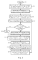
Please refer to FIG. 2: FIG. 2 is a block diagram of the DVD playback system 200 including a decoding device 230 according to the first embodiment of the present invention. As shown in FIG. 2, the playback system 200 includes an EFM+ demodulator 210, a main data storage device 220 (e.g. Dynamic Random Access Memory), a decoding device 230, a decoding result confirmation unit 240, an ATAPI interface unit 250, and a bus 260. The decoding device 230 includes an error correction unit 231, a data buffer 234, a PI decoding unit 236, and a PO decoding unit 237. The error correction unit 231 includes a PO error information register 233 and a dynamic correction unit 232. At first, the decoding device 230 reads the data from the main data storage device 220 to the error correction unit 231. Since this is the first time to read the data, the error information register 233 does not have any PO-relative error information and error address. The data will therefore be directly sent to the data buffer 234. Next, the decoding device 230 reads the data progressively from the main data storage device 220 according to the PI direction. The data read by the decoding device 230 is continuous data; the main storage device 220 thus avoids the additional burden of discontinuous data reading.
The PI decoding unit 236 decodes and corrects the data stored in the data buffer 234 in sequence according to the PI direction, and generates the PI direction error value and error address. The PI direction error value and error address are then utilized to process a logic calculation (normally an XOR calculation) with the data corresponding to the error address. The correct data generated from the calculation is rewritten into the data buffer 234 to finish the operation of the PI direction error correction. The PI corrected data is then written into the main data storage device 220. Additionally, the PO decoding unit 237 decodes the data stored in the data buffer 234 according to the PO direction to generate the PO direction error value and error address, and then sends the PO direction error value and error address to the PO error information register 233 of the error correction unit 231. In the next accessing, the decoding device 230 reads the data in sequence according to the PI direction from the main data storage device 220, and sends the data into the error correction unit 231. At this moment, since the error information register 233 already contains the PO error information and error address, the dynamic correction unit 232 is able to correct the data according to the PO direction and write the corrected data into the main data storage device 220. The decoding result confirmation unit 240 reads data from the main data storage device 220 and checks if the operation of error correction is completed. Finally the ATAPI interface unit 250 sends the corrected data from the main data storage device 220 to a host in order to execute the following data processing schedule.
In this preferred embodiment, the data buffer 234 is utilized for registering and buffering the data from the error correction unit 231 and for PI direction decoding and PO direction decoding. With the assistance of the error correction unit 231, the data stored in the data buffer 234 can finally be rewritten in sequence into the main data storage device 220. Please note that, in this moment; the data buffer 234 writes the whole data (including the error corrected data, the data with indeterminable errors, and the originally correct data) into the main data storage device 220 in sequence. Thus, the decoding device 230 in the present invention does not need to write the corrected data randomly into the main storage device 220 as in the related art. Therefore the decoding device 230 in the present invention reduces the bandwidth and access time of the main data storage device 220 and increases the data access efficiency of the main data storage device 220.
Please refer to FIG. 3. Please refer to FIG. 3: FIG. 3 shows a flowchart illustrating the data decoding and error correction operation of the decoding device 230 shown in FIG. 2. Related steps shown in the flow chart do not necessarily need to be sequentially executed; other steps may be inserted between the present steps. In general, however, the results are the same. The processes of data decoding and error correction are detailed in the following:
Step 300: Start.
Step 302: The decoding device 230 reads a plurality of un-decoded data from the main data storage device 220 in sequence according to the PI direction, and stores each un-decoded data progressively into the data buffer 234.
Step 304: The PI decoding unit 236 decodes the data stored in the data buffer 234 in sequence according to the PI direction, utilizes the decoded PI direction error value and error address to process a logic calculation (normally an XOR calculation) with the data corresponding to the error address, and rewrites the calculated data into the data buffer 234 to finish the PI direction error correction process.
Step 306: The PO decoding unit 237 decodes the data stored in the data buffer 234 according to the PO direction, generates the PO direction error value and error address and registers the PO direction error value and error address to the PO error information register 233.
Step 308: The data buffer 234 writes its registered data in sequence back into the main data storage device 220 according to the PI direction.
Step 310: The decoding device 240 determines whether the data correction is completed and correct by checking the data stored in the data storage device 220. If the correction is completed, the process goes to step 312.
Step 312: The decoding device 230 reads a plurality of un-decoded data from the main data storage device 220 in sequence according to the PI direction.
Step 314: The dynamic correction unit 232 processes each un-decoded data progressively, corrects the error portion of each un-decoded data according to the error value and error address stored in the PO error information register 233, and then writes the processed un-decoded data into the data buffer 234.
Step 316: The PI decoding unit 236 decodes the data stored in the data buffer 234 in sequence according to the PI direction, utilizes the decoded PI direction error value and error address to process a logic calculation (normally an XOR calculation) with the data corresponding to the error address, and rewrites the calculated data into the data buffer 234 to finish the PI direction error correction process.
Step 318: The PO decoding unit 237 decodes the data stored in the data buffer 234 according to the PO direction, generates the PO direction error value and error address, and registers the PO direction error value and error address to the PO error information register 233.
Step 320: The data buffer 234 writes the stored data into the main data storage device 220 in sequence according to the PI direction, and then goes back to step 310.
Step 322: End.
Please refer to FIG. 4 and FIG. 5: FIG. 4 is a block diagram of the DVD playback system 400 including a decoding device 430 according to the second embodiment of the present invention; FIG. 5 is a block diagram of the DVD playback system 500 including a decoding device 530 according to the third embodiment of the present invention. Please note that, since the same name elements of the DVD playback system 200, 400 and 500 shown in FIG. 2, FIG. 4 and FIG. 5 have the same function and operation, detailed description is omitted for the sake of brevity. The difference between the DVD playback system 400 as shown in FIG. 4 and the DVD playback system 200 as shown in FIG. 2 is that the PI decoding unit 436 of the decoding device 430 directly receives each un-decoded data from the main data storage device 220, and processes the operation of decoding and correcting the data according to the PI direction and error correction. After decoding and correcting, the corrected data will be sent into the data buffer 234. In contrast to the DVD playback system 200, the DVD playback system 400 therefore reduces the data access frequency and lowers the bandwidth requirement for the data buffer 234. Moreover, the difference between the DVD playback system 500 shown in FIG. 5 and the DVD playback system 400 shown in FIG. 4 is that the decoding result confirmation unit 540 is directly coupled to the data buffer 234. Therefore, when the data stored in the data buffer 234 (already processed by the decoding device 530) is rewritten into the main data storage device 220, the decoding result confirmation unit 540 is able to receive the data stored in the data buffer 234 simultaneously and to determine whether the error correction process is completed. In other words, the decoding result confirmation unit 540 does not need to read the data rewritten by the data buffer 234 from the main data storage device 220 through the bus 260. Accordingly, the DVD playback system can greatly reduce the data access frequency, as well as the bandwidth consumption, of the main data storage device 220.
In the embodiments detailed above, the data buffer 234 writes the whole stored data (including the error corrected data, the data with indeterminable error, and the originally correct data) into the main data storage device 220 in sequence. If only a few data have errors (i.e. most of the data in the main data storage device 220 are correct), only the corrected data need to be rewritten into the main data storage device 220 in order to reduce the required memory bandwidth. In this situation, the present invention further provides a data rewritten mechanism to determine whether to write the whole data in sequence or to only write the corrected data back to the main data storage device 220 according to different data error quantities.
Please refer to FIG. 6: FIG. 6 is a block diagram of the DVD playback system 600 including a decoding device 630 according to the fourth embodiment of the present invention. Please note that, since the same name elements of the DVD playback system 200 and 600 shown in FIG. 2 and FIG. 6 have the same function and operation, detailed description is omitted for the sake of brevity. In contrast to the DVD playback system 200 shown in FIG. 2, the DVD playback system 600 additionally sets a correction flag buffer 610 and a rewriting unit 620. When the PI decoding unit 236 processes the operation of the PI direction error correction to the data inputted into the decoding device 630, the PI decoding unit 236 sets an error correction flag stored in the correction flag buffer 610 according to the location of the corrected data. That is, when the dynamic correction unit 232 processes the error correction operation to the data inputted into the decoding device 630, the dynamic correction unit 232 also sets an error correction flag stored in the correction flag buffer 610 according to the location of the corrected data. In other words, the error correction flag is utilized for indicating a data section stored in the data buffer 234 that has been error corrected.
The size of the data section can be adjusted according to design requirements. For example, each error correction flag (1 bit) can mark the data with one byte to recognize if the data is error corrected. Thus, for each data corresponding to the PI direction (e.g. the PI codeword is 182 bytes in length), the correction flag buffer 610 stores 128 error correction flags. That is, when the number “n” byte of the data is error corrected, the number “n” error correction flag of the 128 error correction flags then will be marked as a first flag value (e.g. the logical value “1”). When the number n+1 byte of the data corresponding to the PI direction is not error corrected, the number n+1 error correction flag of the 128 error correction flags will therefore be marked with another flag value (e.g. the logical value “0”). Furthermore, in order to reduce the required memory capacity of the error flag buffer, the length of each data section corresponding to the error correction flag can be determined according to the hardware structure of the main data storage device 220. For example, the main data storage device can access 32 bits (4 bytes) in each clock cycle, and therefore one error correction flag (1 bit) can mark the data with 4 bytes to recognize if the data is error corrected. Finally, the rewriting unit 620 can determine the data rewriting mechanism according to the error correction flag recorded in the correction flag buffer 610. If the quantity of error data is more than a threshold value, meaning the error data is too much, the rewriting unit 620 can write the whole data stored in the data buffer 234 back to the main data storage device 220 according to the rewriting mechanism of the above embodiments. If the quantity of error data is less than the threshold value, however, the rewriting unit 620 can, as in the conventional method, randomly write the data section, which is error corrected and stored in the data buffer 234, back to the main data storage device 220 according to the error correction flag in the correction flag buffer 610.
Please refer to FIG. 7: FIG. 7 is a block diagram of the first embodiment of the rewriting unit 620 shown in FIG. 6. As shown in FIG. 7, the rewriting unit 620 includes a rewriting buffer 622, a counter 624, and a switch module 626. The rewriting buffer 622 is utilized to store the data section (at least including the corrected data) and the related address information, which is ready to be rewritten to the main data storage device 220. The switch module 626 determines whether to couple the data buffer 234 and the counter 624 to the rewriting buffer 622 according to each error correction flag in the correction flag buffer 610. That is, the error correction flag is utilized as an enable signal for the switch module 626. The counter 624 is utilized to count each un-decoded unit of an un-decoded data corresponding to the PI direction stored in the data buffer 234 to generate an address value. For instance, for a PI codeword, the counter 624 counts each symbol of the PI codeword to generate the corresponding address value. Thus when an error correction flag, which indicates the location of error correction, enables the switch module 626, the address value outputted from the counter 624 and the corresponding data section stored in the data buffer 234 are written back into the rewriting module 622 altogether.
Please refer to FIG. 8: FIG. 8 is a block diagram of the second embodiment of the rewriting unit 620 shown in FIG. 6. As shown in FIG. 8, the rewriting unit 620 includes an encoder 627, a data fetch unit 628 and a rewriting buffer 629. The rewriting buffer 629 is utilized to store the data section (at least including the corrected data) and the related address information, which is ready to be rewritten to the main data storage device 220. The encoder 627 directly encodes each error correction flag of the correction flag buffer 610 to generate the address information corresponding to a data section, writes the address information of the data section into the rewriting buffer 629, and sends the address information to the data fetch unit 628. The data fetch unit 628 can thus acquire the data section from the data buffer 234 according to the address information of the data section outputted by the encoder 627, and write the data section back to the rewriting buffer 629.
Please refer to FIG. 9 and FIG. 10: FIG. 9 is a block diagram of the DVD playback system 900 including a decoding device 930 according to the fifth embodiment of the present invention; FIG. 10 is a block diagram of the DVD playback system 1000 including a decoding device 1030 according to the sixth embodiment of the present invention. Please note that, since the same name elements of the DVD playback system 900 and 400 shown in FIG. 9 and FIG. 4 have the same function and operation, and the elements of the same name of the DVD playback system 1000 and 500 shown in FIG. 10 and FIG. 5 have the same function and operation, detailed description is omitted for the sake of brevity. In contrast to the DVD playback system 400, the DVD playback system 900 sets the above-mentioned correction flag buffer 610 and rewriting unit 620 in the decoding device 930. Similarly, in contrast to the DVD playback system 500, the DVD playback system 1000 sets the above-mentioned correction flag buffer 610 and rewriting unit 620 in the decoding device 1030.
In contrast to the related art, the decoding devices of the present invention and the related decoding methods process the error correction to each error data according to the error correction information of the PO direction during reception of a plurality of un-decoded data according to the PI direction. Thus this invention resolves the problem of a conventional error correction process where the PO direction is required to access the main data storage device randomly. That is, the decoding devices and the decoding methods of the present invention improve the efficiency of the main data storage device. Moreover, the decoding devices and the decoding methods of the present invention are able to determine the rewriting mode according to the quantity of data error. Thus the bandwidth distribution flexibility of the main data storage device is greatly improved.
Those skilled in the art will readily observe that numerous modifications and alterations of the device and method may be made while retaining the teachings of the invention. Accordingly, the above disclosure should be construed as limited only by the metes and bounds of the appended claims.

Claims (19)

1. A decoding device for processing an uncorrected data in a data storage medium, the uncorrected data comprising a first direction error data and a second direction error data, the decoding device comprising:
an error correction unit, receiving the uncorrected data, for correcting the second direction error data of the uncorrected data according to a second direction decoding information and outputting a data;
a data buffer, coupled to the error correction unit, for buffering the data and outputting a corrected data after the first direction error data of the data is corrected;
a first decoding unit, coupled to the data buffer, for decoding and correcting the first direction error data of the data stored in the data buffer; and
a second decoding unit, coupled to the data buffer and the error correction unit, for generating the second direction decoding information to the error correction unit according to the data stored in the data buffer.
2. The decoding device of claim 1, wherein the error correction unit comprises:
a register, receiving the second direction decoding information, for storing the second direction error data and a memory address of the second direction error data; and a dynamic correction unit for correcting the uncorrected data according to the second direction error data and the memory address of the second direction error data stored in the register.
3. The decoding device of claim 1, wherein the data buffer is coupled to a detecting unit, and the detecting unit is utilized for checking the corrected data outputted from the data buffer.
4. The decoding device of claim 1, further comprising:
a flag buffer, coupled to the first decoding unit, for storing a flag signal; and
a rewriting unit, coupled to the data buffer, the flag buffer and the data storage medium, for determining a rewriting mode of the data storage medium according to the data of the data buffer and the flag signal of the flag buffer.
5. The decoding device of claim 4, wherein the rewriting unit comprises:
a rewriting buffer for storing an error data, which is ready to be rewritten into the data storage medium, and storing a memory location of the storage medium corresponding to the error data;
a counter for counting the memory location of the data storage medium; and
a switch module, coupled to the rewriting buffer and the counter, for controlling the error data and the memory location to store in the rewriting buffer.
6. The decoding device of claim 4, wherein the rewriting unit comprises:
a rewriting buffer for storing an error data, which is ready to be rewritten to the data storage medium, and storing a memory location of the storage medium corresponding to the error data;
an encoder, coupled to the rewriting buffer, for generating the memory location according to the flag signal and writing the memory location to the rewriting buffer;
a data fetch unit, coupled to the encoder and the rewriting buffer, for outputting the error data according to the memory location outputted by the encoder.
7. The decoding device of claim 1, wherein the data buffer is coupled to a detecting unit, and the detecting unit is utilized for checking the corrected data outputted from the data buffer.
8. The decoding device of claim 1, wherein the first direction error data is an inner-code parity direction error data; and the second direction error data is an outer-code parity direction data.
9. A decoding device for processing an uncorrected data in a data storage medium, the uncorrected data comprising a first direction error data and a second direction error data, the decoding device comprising:
an error correction unit, receiving the uncorrected data, for correcting the second direction error data of the uncorrected data according to a second direction decoding information and outputting a data;
a first decoding unit, coupled to the error correction unit, for decoding the first direction error data of the data to output a first data;
a data buffer, coupled to the first decoding unit, for buffering the first data and outputting a corrected data after the first direction error data of the first data is corrected; and
a second decoding unit, coupled to the data buffer and the error correction unit, for generating the second direction decoding information to the error correction unit according to the first data stored in the data buffer.
10. The decoding device of claim 9, wherein the error correction unit comprises:
a register, receiving the second direction decoding information, for storing the second direction error data and a memory address of the second direction error data; and
a dynamic correction unit for correcting the uncorrected data according to the second direction error data and the memory address of the second direction error data stored in the register.
11. The decoding device of claim 9, further comprising:
a flag buffer, coupled to the first decoding unit, for storing a flag signal; and
a rewriting unit, coupled to the data buffer, the flag buffer and the data storage medium, for determining a rewriting mode of the data storage medium according to the data of the data buffer and the flag signal of the flag buffer.
12. The decoding device of claim 11, wherein the rewriting unit comprises:
a rewriting buffer for storing an error data, which is ready to be rewritten into the data storage medium, and storing a memory location of the storage medium corresponding to the error data;
a counter for counting the memory location of the data storage medium; and
a switch module, coupled to the rewriting buffer and the counter, for controlling the error data and the memory location to store in the rewriting buffer.
13. The decoding device of claim 11, wherein the rewriting unit comprises:
a rewriting buffer for storing an error data, which is ready to be rewritten into the data storage medium, and storing a memory location of the storage medium corresponding to the error data;
an encoder, coupled to the rewriting buffer, for generating the memory location according to the flag signal and writing the memory location to the rewriting buffer;
a data fetch unit, coupled to the encoder and the rewriting buffer, for outputting the error data according to the memory location outputted by the encoder.
14. The decoding device of claim 9, wherein the data buffer is coupled to a detecting unit, and the detecting unit is utilized for checking the corrected data outputted from the data buffer.
15. The decoding device of claim 9, wherein the first direction error data is an inner-code parity direction error data; and the second direction error data is an outer-code parity direction data.
16. A decoding method for processing an uncorrected data in a data storage medium, comprising:
receiving the uncorrected data according to a first direction of the data medium and storing the uncorrected data into a buffer;
correcting a first direction error of the uncorrected data stored in the buffer according to a first direction decoding and correction information, and generating a second direction decoding and correction information to an error correction unit;
receiving the uncorrected data to the error correction unit according to the first direction of the data storage medium, and correcting a second direction error of the uncorrected data according to the second direction decoding and correction information; and
checking whether the first and second direction error of the uncorrected data are corrected.
17. The decoding method of claim 16, further comprising:
generating a first direction flag to a rewriting unit according to the uncorrected data to determine the rewriting mode of rewriting the uncorrected data to the data storage medium.
18. The decoding method of claim 16, wherein the second direction decoding and correction information comprises a second direction error value and a memory location of the second direction error value.
19. The decoding method of claim 16, wherein the first direction error is an inner-code parity direction error data; and the second direction error is an outer-code parity direction data.
US11/558,927 2005-11-24 2006-11-12 Decoding device in optical disc drive and related decoding method thereof Active 2029-02-18 US7797608B2 (en)

Applications Claiming Priority (3)

Application Number Priority Date Filing Date Title
TW94141274A 2005-11-24
TW094141274 2005-11-24
TW094141274A TWI282087B (en) 2005-11-24 2005-11-24 Decoding device in optical disc drive and related decoding method thereof

Publications (2)

Publication Number Publication Date
US20070118789A1 US20070118789A1 (en) 2007-05-24
US7797608B2 true US7797608B2 (en) 2010-09-14

Family

ID=37636336

Family Applications (1)

Application Number Title Priority Date Filing Date
US11/558,927 Active 2029-02-18 US7797608B2 (en) 2005-11-24 2006-11-12 Decoding device in optical disc drive and related decoding method thereof

Country Status (3)

Country Link
US (1) US7797608B2 (en)
GB (1) GB2432691B (en)
TW (1) TWI282087B (en)

Cited By (3)

* Cited by examiner, † Cited by third party
Publication number Priority date Publication date Assignee Title
US20070260960A1 (en) * 2006-04-21 2007-11-08 Kuo-Lung Chien Error correction system and related method thereof
US20070260961A1 (en) * 2006-04-21 2007-11-08 Kuo-Lung Chien Error correction system and related method thereof
US20070260963A1 (en) * 2006-04-21 2007-11-08 Kuo-Lung Chien Error correction system and related method thereof

Families Citing this family (2)

* Cited by examiner, † Cited by third party
Publication number Priority date Publication date Assignee Title
US20080057877A1 (en) * 2006-08-31 2008-03-06 Motorola, Inc. System and method to rapidly deploy one or more communication devices
KR100953657B1 (en) * 2007-11-13 2010-04-20 삼성모바일디스플레이주식회사 Thin film transistors, fabricating method of the same and organic light emitting diode device using the same

Citations (10)

* Cited by examiner, † Cited by third party
Publication number Priority date Publication date Assignee Title
JPS61270922A (en) 1985-05-25 1986-12-01 Sony Corp Decoder for error correction code
US5696774A (en) * 1994-12-01 1997-12-09 Mitsubishi Denki Kabushiki Kaisha Digital signal recording device, digital signal playback device, and digital signal decoding device therefor
JPH11282703A (en) 1998-03-27 1999-10-15 Nec Corp Device and method for error correction
US5996105A (en) * 1997-11-14 1999-11-30 Cirrus Logic, Inc. ECC system employing a data buffer for storing codeword data and a syndrome buffer for storing error syndromes
US6029266A (en) * 1996-08-06 2000-02-22 Samsung Electronics Co., Ltd. Error correcting apparatus and method of digital processing system for correcting general and erasure errors
US6158038A (en) * 1996-11-15 2000-12-05 Fujitsu Limited Method and apparatus for correcting data errors
US6662335B1 (en) 2000-01-25 2003-12-09 Mediatek Inc. Method and apparatus for accessing DVD data
US6742157B2 (en) 2000-10-23 2004-05-25 Acer Laboratories Inc. Decoding system and method in an optical disk storage device
US6742156B2 (en) 2000-12-15 2004-05-25 Acer Laboratories Inc. Decoding system and method in an optical disk storage device
US6772385B2 (en) 2000-01-31 2004-08-03 Sanyo Electric Co., Ltd. Error-correcting device and decoder enabling fast error correction with reduced circuit scale

Patent Citations (10)

* Cited by examiner, † Cited by third party
Publication number Priority date Publication date Assignee Title
JPS61270922A (en) 1985-05-25 1986-12-01 Sony Corp Decoder for error correction code
US5696774A (en) * 1994-12-01 1997-12-09 Mitsubishi Denki Kabushiki Kaisha Digital signal recording device, digital signal playback device, and digital signal decoding device therefor
US6029266A (en) * 1996-08-06 2000-02-22 Samsung Electronics Co., Ltd. Error correcting apparatus and method of digital processing system for correcting general and erasure errors
US6158038A (en) * 1996-11-15 2000-12-05 Fujitsu Limited Method and apparatus for correcting data errors
US5996105A (en) * 1997-11-14 1999-11-30 Cirrus Logic, Inc. ECC system employing a data buffer for storing codeword data and a syndrome buffer for storing error syndromes
JPH11282703A (en) 1998-03-27 1999-10-15 Nec Corp Device and method for error correction
US6662335B1 (en) 2000-01-25 2003-12-09 Mediatek Inc. Method and apparatus for accessing DVD data
US6772385B2 (en) 2000-01-31 2004-08-03 Sanyo Electric Co., Ltd. Error-correcting device and decoder enabling fast error correction with reduced circuit scale
US6742157B2 (en) 2000-10-23 2004-05-25 Acer Laboratories Inc. Decoding system and method in an optical disk storage device
US6742156B2 (en) 2000-12-15 2004-05-25 Acer Laboratories Inc. Decoding system and method in an optical disk storage device

Cited By (3)

* Cited by examiner, † Cited by third party
Publication number Priority date Publication date Assignee Title
US20070260960A1 (en) * 2006-04-21 2007-11-08 Kuo-Lung Chien Error correction system and related method thereof
US20070260961A1 (en) * 2006-04-21 2007-11-08 Kuo-Lung Chien Error correction system and related method thereof
US20070260963A1 (en) * 2006-04-21 2007-11-08 Kuo-Lung Chien Error correction system and related method thereof

Also Published As

Publication number Publication date
GB2432691A (en) 2007-05-30
GB0623309D0 (en) 2007-01-03
GB2432691B (en) 2007-10-10
TWI282087B (en) 2007-06-01
TW200721117A (en) 2007-06-01
US20070118789A1 (en) 2007-05-24

Similar Documents

Publication Publication Date Title
US6662334B1 (en) Method and device for performing error correction on ECC data sectors
US6192499B1 (en) Device and method for extending error correction beyond one sector time
KR100370239B1 (en) Memory device for applying to high speed block pipelined reed-solomon decoder and method of memory access and reed-solomon decoder having the memory device
US7600177B2 (en) Delta syndrome based iterative Reed-Solomon product code decoder
US6363511B1 (en) Device and method for decoding data streams from storage media
CN1779838B (en) Digital signal processing method and apparatus performing variable number of error correction repetitions
US6378103B1 (en) Apparatus and method for error correction in optical disk system
KR100430657B1 (en) Signal processor for correcting and detecting errors
JP3239863B2 (en) Data decoding processing apparatus and method
US7624330B2 (en) Unified memory architecture for recording applications
US7797608B2 (en) Decoding device in optical disc drive and related decoding method thereof
US20060259850A1 (en) Error correcting apparatus
US7007222B2 (en) Apparatus for accessing data stored on an optical disc
JP4819843B2 (en) ECC code generation method for memory device
US8181075B2 (en) Error correction device and recording and reproducing device
US20070150798A1 (en) Method for decoding an ecc block and related apparatus
US7774676B2 (en) Methods and apparatuses for generating error correction codes
US7823045B2 (en) Error correction apparatus and method thereof
JP2004080762A (en) Method and equipment performing cross interleave reed-solomon code correction
US20080109706A1 (en) Error correction method and apparatus for optical information storage medium recording/reproducing apparatus
US7555698B2 (en) Method and apparatus for extracting specific data from BIS data
JP2005216477A (en) Method and device for decoding dvd using selective po correction
US6694473B1 (en) Parallel signal decoding method
US20060218468A1 (en) Memory initialization device, memory initialization method, and error correction device
US20060282746A1 (en) Method and apparatus for accessing data stored on an optical disc

Legal Events

Date Code Title Description
AS Assignment

Owner name: REALTEK SEMICONDUCTOR CORP., TAIWAN

Free format text: ASSIGNMENT OF ASSIGNORS INTEREST;ASSIGNORS:CHANG, HUI-HUANG;CHEN, CHIEN-CHIH;REEL/FRAME:018508/0837

Effective date: 20061105

STCF Information on status: patent grant

Free format text: PATENTED CASE

FPAY Fee payment

Year of fee payment: 4

MAFP Maintenance fee payment

Free format text: PAYMENT OF MAINTENANCE FEE, 8TH YEAR, LARGE ENTITY (ORIGINAL EVENT CODE: M1552)

Year of fee payment: 8

MAFP Maintenance fee payment

Free format text: PAYMENT OF MAINTENANCE FEE, 12TH YEAR, LARGE ENTITY (ORIGINAL EVENT CODE: M1553); ENTITY STATUS OF PATENT OWNER: LARGE ENTITY

Year of fee payment: 12