US7777512B2 - Semiconductor device - Google Patents
Semiconductor device Download PDFInfo
- Publication number
- US7777512B2 US7777512B2 US12/042,956 US4295608A US7777512B2 US 7777512 B2 US7777512 B2 US 7777512B2 US 4295608 A US4295608 A US 4295608A US 7777512 B2 US7777512 B2 US 7777512B2
- Authority
- US
- United States
- Prior art keywords
- circuit
- power supply
- inverting amplifier
- fluctuation detection
- voltage fluctuation
- Prior art date
- Legal status (The legal status is an assumption and is not a legal conclusion. Google has not performed a legal analysis and makes no representation as to the accuracy of the status listed.)
- Expired - Fee Related, expires
Links
- 239000004065 semiconductor Substances 0.000 title claims abstract description 154
- 238000001514 detection method Methods 0.000 claims abstract description 133
- 238000007689 inspection Methods 0.000 claims description 35
- 238000000034 method Methods 0.000 claims description 21
- 238000004458 analytical method Methods 0.000 claims description 12
- 238000012360 testing method Methods 0.000 claims description 12
- 238000004088 simulation Methods 0.000 claims description 5
- 238000009877 rendering Methods 0.000 claims description 2
- 238000010586 diagram Methods 0.000 description 19
- 230000006870 function Effects 0.000 description 16
- 238000013461 design Methods 0.000 description 10
- 230000008859 change Effects 0.000 description 7
- 230000007274 generation of a signal involved in cell-cell signaling Effects 0.000 description 5
- 230000007704 transition Effects 0.000 description 5
- 230000000694 effects Effects 0.000 description 4
- 238000012545 processing Methods 0.000 description 4
- 230000008569 process Effects 0.000 description 3
- 230000004075 alteration Effects 0.000 description 2
- 230000008901 benefit Effects 0.000 description 2
- 230000007547 defect Effects 0.000 description 2
- 230000002950 deficient Effects 0.000 description 2
- 238000005259 measurement Methods 0.000 description 2
- 238000012986 modification Methods 0.000 description 2
- 230000004048 modification Effects 0.000 description 2
- 238000004806 packaging method and process Methods 0.000 description 2
- 239000000047 product Substances 0.000 description 2
- 230000001052 transient effect Effects 0.000 description 2
- 230000009471 action Effects 0.000 description 1
- 238000011161 development Methods 0.000 description 1
- 239000012467 final product Substances 0.000 description 1
- 238000007429 general method Methods 0.000 description 1
- 238000004519 manufacturing process Methods 0.000 description 1
- 230000008520 organization Effects 0.000 description 1
- 230000009467 reduction Effects 0.000 description 1
Images


Classifications
-
- G—PHYSICS
- G01—MEASURING; TESTING
- G01R—MEASURING ELECTRIC VARIABLES; MEASURING MAGNETIC VARIABLES
- G01R31/00—Arrangements for testing electric properties; Arrangements for locating electric faults; Arrangements for electrical testing characterised by what is being tested not provided for elsewhere
- G01R31/28—Testing of electronic circuits, e.g. by signal tracer
- G01R31/2851—Testing of integrated circuits [IC]
- G01R31/2884—Testing of integrated circuits [IC] using dedicated test connectors, test elements or test circuits on the IC under test
-
- G—PHYSICS
- G01—MEASURING; TESTING
- G01R—MEASURING ELECTRIC VARIABLES; MEASURING MAGNETIC VARIABLES
- G01R19/00—Arrangements for measuring currents or voltages or for indicating presence or sign thereof
- G01R19/165—Indicating that current or voltage is either above or below a predetermined value or within or outside a predetermined range of values
- G01R19/16533—Indicating that current or voltage is either above or below a predetermined value or within or outside a predetermined range of values characterised by the application
- G01R19/16538—Indicating that current or voltage is either above or below a predetermined value or within or outside a predetermined range of values characterised by the application in AC or DC supplies
- G01R19/16552—Indicating that current or voltage is either above or below a predetermined value or within or outside a predetermined range of values characterised by the application in AC or DC supplies in I.C. power supplies
Definitions
- the present invention relates to a semiconductor device with a voltage fluctuation detection circuit for detecting fluctuations in power supply voltage caused in a semiconductor chip.
- an input/output interface circuit might experience an operational failure.
- Examples of the cause of a significant reduction in power supply voltage include the following cases: defective design of the semiconductor chip, which causes high current to flow locally, resulting in a voltage drop; and partial disconnection of wiring between a terminal of the power supply and a terminal of the semiconductor chip during packaging, which causes the power supply voltage to drop by more than a design value.
- FIG. 21 illustrates the configuration of the semiconductor device 50 described in the above prior art document.
- the semiconductor device 50 includes a normal circuit 51 , and a voltage fluctuation detection device 52 .
- the voltage fluctuation detection device 52 includes an inverting amplifier 53 and a latching circuit 54 .
- the inverting amplifier 53 is connected between a terminal 521 for an external power supply 500 that supplies power to the normal circuit 51 and a terminal 522 to which a ground potential VSS is supplied.
- the latching circuit 54 has a reset terminal connected to an output terminal of the inverting amplifier 53 .
- the normal circuit 51 refers to one of the circuits included in the semiconductor device 50 that is used during normal operation and has any portions used only for inspection excluded therefrom.
- the potential of the external power supply 500 is denoted by VDD
- the power supply voltage of the normal circuit 51 is denoted by Vc.
- VDD of the external power supply 500 normally shows a constant value
- the power supply voltage Vc applied from the external power supply 500 to the normal circuit 51 changes in accordance with the operation of the normal circuit 51 . The same applies to the following descriptions.
- a reference voltage VDC is supplied from an external power supply (not shown) to an input terminal 55 of the inverting amplifier 53 .
- an output from the latching circuit 54 is inverted. Accordingly, based on the output from the latching circuit 54 , it is possible to detect whether the power supply voltage Vc is below the reference voltage VDC.
- the above conventional device is not capable of detecting the value of the power supply voltage Vc at arbitrary times during the operation of the normal circuit 51 . In other words, any fluctuations in power supply voltage over time cannot be detected, and therefore there is a limit in the ability to analyze the behavior of semiconductor devices.
- the above conventional device requires wiring for analog signals because an analog signal is inputted from the terminal 55 as the reference voltage VDC. Since the wiring for analog signals is susceptible to influences of resistance and noise compared to wiring compatible with digital signals, it is necessary to design the device considering such aspects, which leads to a relative increase in size. As a result, the wiring for detecting voltage fluctuations disadvantageously imposes constraints on the design of semiconductor chips.
- An object of the present invention is to provide a semiconductor device that is capable of readily detecting the value of the power supply voltage at arbitrary times during the operation of the normal circuit, but does not require any wiring and terminals for analog signals.
- the present invention provides a semiconductor device comprising:
- a voltage fluctuation detection circuit for detecting fluctuations in a voltage applied from an external power supply to the normal circuit
- the voltage fluctuation detection circuit includes:
- the present invention provides a method for testing the semiconductor device, comprising:
- the semiconductor device of the present invention By employing the semiconductor device of the present invention and the method for testing the same, it becomes possible to readily detect the value of the power supply voltage at any arbitrary times during the operation of the normal circuit, which is an advantage in analyzing the semiconductor device operation.
- the semiconductor device of the present invention does not require any reference voltage to be inputted, and therefore it is possible to eliminate the necessity of any wiring and terminals for analog signals, and reduce constraints on the design of semiconductor chips.
- FIG. 1 is a circuit diagram illustrating the configuration of a semiconductor device according to a first embodiment of the present invention.
- FIG. 2 is a graph for describing a power supply voltage detection method using the semiconductor device according to the first embodiment.
- FIGS. 3A to 3D are graphs for describing the power supply voltage detection method using the semiconductor device according to the first embodiment.
- FIG. 4 is a circuit diagram illustrating the configuration of a semiconductor device according to a second embodiment of the present invention.
- FIGS. 5A and 5B are graphs for describing a power supply voltage detection method using the semiconductor device according to the second embodiment.
- FIG. 6 is a circuit diagram illustrating the configuration of a semiconductor device according to a third embodiment of the present invention.
- FIG. 7 is a circuit diagram illustrating the configuration of a semiconductor device according to a fourth embodiment of the present invention.
- FIG. 8 is a circuit diagram illustrating the configuration of a semiconductor device according to a fifth embodiment of the present invention.
- FIG. 9 is a circuit diagram illustrating the configuration of a semiconductor device according to a sixth embodiment of the present invention.
- FIG. 10 is a circuit diagram illustrating the configuration of a semiconductor device according to a seventh embodiment of the present invention.
- FIG. 11 is a circuit diagram illustrating the configuration of a semiconductor device according to an eighth embodiment of the present invention.
- FIG. 12 is a graph for describing a power supply voltage detection method using the semiconductor device according to the eighth embodiment.
- FIG. 13 is a circuit diagram illustrating the configuration of a semiconductor device according to a ninth embodiment of the present invention.
- FIG. 14 is a circuit diagram illustrating the configuration of a semiconductor device according to a tenth embodiment of the present invention.
- FIG. 15 is a circuit diagram illustrating the configuration of a semiconductor device according to an eleventh embodiment of the present invention.
- FIG. 16 is a diagram for describing a method for placing semiconductor devices on a semiconductor chip according to a twelfth embodiment of the present invention.
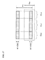
- FIG. 17 is a diagram for describing a semiconductor device layout method according to a thirteenth embodiment of the present invention.
- FIG. 18 is a circuit diagram illustrating the configuration of a semiconductor device according to a fourteenth embodiment of the present invention.
- FIG. 19 is a circuit diagram illustrating the configuration of a semiconductor device according to a fifteenth embodiment of the present invention.
- FIG. 20 is a diagram illustrating the configurations of libraries for semiconductor devices according to a sixteenth embodiment of the present invention.
- FIG. 21 is a circuit diagram illustrating the configuration of a conventional semiconductor device.
- FIG. 1 illustrates the configuration of a semiconductor device according to a first embodiment of the present invention.
- the semiconductor device 10 a includes a normal circuit 11 and a voltage fluctuation detection circuit 12 a , as shown in FIG. 1 .
- the normal circuit 11 is one of the circuits included in the semiconductor device 10 a that is used during normal operation, i.e., the circuit has any portions used only for inspection excluded therefrom. In addition, the normal circuit 11 functions when the semiconductor device 10 a is mounted in a final product.
- the normal circuit 11 is connected to an external power supply (hereinafter, simply referred to as a “power supply”) 100 via a power supply terminal (in the figure, terminal 121 ).
- the voltage fluctuation detection circuit 12 a is also connected to the power supply 100 via the terminal 121 to detect the value of a power supply voltage Vc applied from the power supply 100 to the normal circuit 11 .
- the voltage fluctuation detection circuit 12 a includes an inverting amplifier 13 a , a switching element 14 , and a capacitance element 15 .
- the inverting amplifier 13 a has two input terminals 121 and 122 , and one output terminal 123 .
- the first input terminal 121 is connected to the power supply 100 (potential VDD), and the second input terminal 122 is connected to the capacitance element 15 .
- the switching element 14 is connected between the output terminal 123 and the second input terminal 122 of the inverting amplifier 13 a .
- the capacitance element 15 is connected between the second input terminal 122 of the inverting amplifier 13 a and a terminal 124 that is held at a ground potential VSS used as a reference potential.
- the inverting amplifier 13 a consists of, but is not limited to, one P-type MOS transistor and one N-type MOS transistor.
- the first input terminal 121 of the inverting amplifier 13 a is connected to a terminal for connecting to the external power supply, but this is not restrictive.
- the first input terminal 121 may be connected to a part of the wiring extending between the normal circuit 11 and the terminal for connecting to the external power supply. The same applies to the subsequent embodiments.
- ON/OFF timing of the switching element 14 can be arbitrarily adjusted by a control means (not shown) provided outside the semiconductor device 10 a and connected to a terminal 31 .
- FIG. 2 is a graph showing the relationship between the power supply voltage Vc (vertical axis) of the semiconductor device 10 a and time (horizontal axis).
- a control signal S 3 from the unillustrated control means is inputted to the normal circuit 11 , starting the operation of the normal circuit 11 .
- the switching element 14 has been previously set to ON state in accordance with a control signal S 1 from the unillustrated control means, and therefore charge corresponding to the power supply voltage Vc accumulates in the capacitance element 15 .
- the power supply voltage Vc fluctuates in accordance with the operation of the normal circuit 11
- the amount of charge accumulating in the capacitance element 15 changes in accordance with the fluctuations.
- voltages at two ends of the capacitance element 15 are about 1 ⁇ 2 of the power supply voltage Vc.
- the normal circuit 11 transitions from an operating state to a suspended state at time Ta 3 .
- the amount of current consumed in the normal circuit 11 and the transient current change significantly decrease, so that the power supply voltage Vc of the normal circuit 11 is rendered equivalent to the potential VDD of the power supply 100 .
- the potential VDD of the power supply 100 is set at an arbitrary value for a time period from time Ta 4 to time Ta 5 , and an output signal of the voltage fluctuation detection circuit 12 a outputted to the terminal 32 is determined.
- the second input terminal 122 of the inverting amplifier 13 a holds a voltage (about 1 ⁇ 2 of Vc 0 ) corresponding to the power supply voltage Vc 0 at time Ta 2 . If the potential VDD of the power supply 100 changes, so that the value of the power supply voltage Vc falls below Vc 0 , the sign (positive/negative) of the output from the voltage fluctuation detection circuit 12 a is inverted. Accordingly, at this time, by measuring the value of the potential VDD of the power supply 100 with a tester or suchlike, it is possible to detect the power supply voltage Vc 0 at time Ta 2 .
- the power supply voltage Vc changes in accordance with the operation status of the normal circuit 11 , whereas during the suspended period (P 2 in FIG. 2 ) of the normal circuit 11 , the power supply voltage Vc has almost the same value as the potential VDD of the power supply 100 .
- the potential VDD of the power supply 100 for the semiconductor device 10 is lowered from its maximum rated value during the suspended period P 2 of the normal circuit 11 , as indicated by the broken lines in the figure, and the value of the potential VDD of the power supply 100 is measured when the output signal of the inverting amplifier 13 a is inverted, making it possible to detect the power supply voltage Vc 0 at time Ta 2 during the operating period P 1 of the normal circuit 11 , i.e., when the switching element 14 changes from ON state to OFF state.
- Ta 6 , Ta 7 , Ta 8 , and Ta 9 it is possible to measure the values Vc 1 , Vc 2 , Vc 3 , and Vc 4 , respectively, of the potential VDD of the power supply 100 when the output signal of the voltage fluctuation detection circuit 12 a is inverted.
- the voltage detection method in the present embodiment does not require any physical processing of the semiconductor device, and therefore the semiconductor device can be used again after inspection.
- the above-described voltage detection method does not require any dedicated reference voltage to be inputted, and any voltage to be referenced is inputted using existing wiring for power supply, thereby eliminating the necessity of any wiring for analog voltage inputs.
- the semiconductor device in the present embodiment can be readily and efficiently mounted on the semiconductor chip.
- FIG. 4 illustrates the configuration of a semiconductor device according to a second embodiment of the present invention.
- the semiconductor device 10 b in FIG. 4 includes a voltage fluctuation detection circuit 12 b , in place of the voltage fluctuation detection circuit 12 a .
- the voltage fluctuation detection circuit 12 b is configured by adding a holding circuit 17 a as a subsequent stage of the inverting amplifier 13 a included in the voltage fluctuation detection circuit 12 a.
- leakage current appears in the capacitance element 15 , and therefore the voltages held at the two ends of the capacitance element 15 drop over time. Accordingly, when it takes time to change the potential VDD of the power supply 100 , the voltages at the two ends of the capacitance element 15 drop during that time, causing errors in detection of the power supply voltage Vc.
- the errors in detection of the power supply voltage Vc are negligible when the value of the leakage current is low, but the reliability of detection results for the power supply voltage Vc deteriorates when the value of the leakage current is high.
- this problem is solved by adding the holding circuit 17 a as a subsequent stage of the inverting amplifier 13 a .
- the time period from T 4 a to T 5 a in which to change the potential VDD of the power supply 100 within the suspended period of the normal circuit 11 , is set to be a predetermined short period after time Ta 2 at which the switching element 14 is set to OFF state.
- an output timing control signal S 4 is inputted from the unillustrated control means to a terminal 33 of the holding circuit 17 a , and an output from the inverting amplifier 13 a at that time is held as an output from the holding circuit 17 a .
- the operation of determining the output from the holding circuit 17 a is repeated while lowering the potential VDD of the power supply 100 from its maximum rated value, as indicated by the broken lines in FIG. 2 . Then, the value of the potential VDD of the power supply 100 is measured when the output from the holding circuit 17 a is inverted.
- the above-described process is repeated while changing the value of time Ta 2 by ⁇ T.
- FIG. 5A shows changes in the power supply voltage Vc during the operating period of the normal circuit 11
- FIG. 5B shows a graph representing determination results obtained by the voltage fluctuation detection circuit 12 b
- the “*” marks denote the values of the potential VDD of the power supply 100 at times when the output of the holding circuit 17 a is inverted.
- FIG. 6 illustrates the configuration of a semiconductor device according to a third embodiment of the present invention.
- the semiconductor device 10 c in FIG. 6 includes a voltage fluctuation detection circuit 12 c , in place of the voltage fluctuation detection circuit 12 a included in the semiconductor device 10 a in FIG. 1 .
- the voltage fluctuation detection circuit 12 c is configured by connecting an amplifier 16 as a subsequent stage of the inverting amplifier 13 a included in the voltage fluctuation detection circuit 12 a.
- the voltage fluctuation detection circuit 12 c has a larger circuit scale than the voltage fluctuation detection circuit according to the configuration in FIG. 1 , but it has an advantage in that smaller voltages can be determined because the output voltage of the inverting amplifier 13 a is amplified.
- FIG. 7 illustrates the configuration of a semiconductor device according to a fourth embodiment of the present invention.
- the semiconductor device 10 d in FIG. 7 includes a voltage fluctuation detection circuit 12 d , in place of the voltage fluctuation detection circuit 12 b included in the semiconductor device 10 b in FIG. 4 .
- the voltage fluctuation detection circuit 12 d is configured by connecting an amplifier 16 between the inverting amplifier 13 a and the holding circuit 17 a included in the voltage fluctuation detection circuit 12 b.
- the voltage fluctuation detection circuit 12 d has an increased circuit scale, but smaller voltages can be determined as in the third embodiment 3. As a result, it is possible to enhance the accuracy in making a graph of fluctuations in the power supply voltage of the normal circuit 11 .
- FIG. 8 illustrates the configuration of a semiconductor device according to a fifth embodiment of the present invention.
- the semiconductor device 10 e in FIG. 8 includes a voltage fluctuation detection circuit 12 e , in place of the voltage fluctuation detection circuit 12 b included in the semiconductor device 10 b in FIG. 4 .
- the voltage fluctuation detection circuit 12 e has an inverting amplifier 13 b configured differently from the inverting amplifier 13 a in FIG. 4 .
- the inverting amplifier 13 b is configured as an NAND circuit by combining two P-type MOS transistors and two N-type MOS transistors.
- the inverting amplifier 13 b is provided with an input terminal 34 for an output fixing control signal S 5 .
- the inverting amplifier 13 b When a “HIGH” signal is inputted from the unillustrated control means to the terminal 34 as the output fixing control signal S 5 , the inverting amplifier 13 b functions in a similar manner to the inverting amplifier 13 a in FIG. 4 . On the other hand, when a “LOW” signal is inputted to the terminal 34 as the output fixing control signal S 5 , the inverting amplifier 13 b does not function as an inverting amplifier.
- FIG. 9 illustrates the configuration of a semiconductor device according to a sixth embodiment of the present invention.
- the semiconductor device 10 f in FIG. 9 includes a voltage fluctuation detection circuit 12 f , in place of the voltage fluctuation detection circuit 12 b included in the semiconductor device 10 b in FIG. 4 .
- the voltage fluctuation detection circuit 12 f differs from the voltage fluctuation detection circuit 12 b in that it additionally has a second capacitance element 18 connected to a power supply 125 for supplying a reference potential REF, via an unillustrated terminal.
- the capacitance elements 15 and 18 are each connected at one terminal to the second input terminal 122 of the inverting amplifier 13 a .
- the capacitance element 15 is connected at the other terminal to a terminal 124 to which the ground potential VSS of the semiconductor device is supplied.
- the capacitance element 18 is connected at the other terminal to the power supply 125 for supplying the reference potential REF.
- reference potential REF may be supplied from inside or outside the semiconductor device, and the same effects can be achieved even when the reference potential REF is the same as the ground potential VSS of the semiconductor device.
- FIG. 10 illustrates the configuration of a semiconductor device according to a seventh embodiment of the present invention.
- the semiconductor device 10 g in FIG. 10 differs from the semiconductor device 10 b in FIG. 4 in that it additionally has an output signal switching circuit 19 .
- the normal circuit 11 and the voltage fluctuation detection circuit 12 b are connected at their respective output terminals to an input terminal of the output signal switching circuit 19 , and an output from either the normal circuit 11 or the voltage fluctuation detection circuit 12 b is outputted to a combined output terminal 35 .
- an output terminal for outputting a predetermined signal for the normal operation during the operation of the normal circuit 11 is combined with an output terminal for outputting output results of the voltage fluctuation detection circuit 12 b , and therefore it is possible to reduce the number of output terminals for inspection.
- the voltage fluctuation detection circuit of the present invention By using the voltage fluctuation detection circuit of the present invention, it becomes possible to detect fluctuations in the power supply voltage during the operating state of the normal circuit 11 with high accuracy, as described in the second embodiment. In addition, by analyzing the behavior of the semiconductor device based on detection results, it becomes possible to determine the range of the power supply voltage that is unlikely to cause any failure, i.e., the tolerable range of the power supply voltage.
- the power supply voltage might fall below the lower limit of the tolerable voltage range due to variations among semiconductor devices caused during the production stage.
- any defect in packaging might result in partial disconnection of the wiring connected to the power supply terminal, causing the power supply voltage to fall below the lower limit of the tolerable voltage range.
- a voltage fluctuation detection circuit suitable for such inspection for shipment is provided.
- FIG. 11 illustrates the configuration of a semiconductor device according to the present embodiment.
- the semiconductor device 10 h in FIG. 11 includes a voltage fluctuation detection circuit 12 g , in place of the voltage fluctuation detection circuit 12 a included in the semiconductor device 10 a in FIG. 1 .
- the voltage fluctuation detection circuit 12 g is configured by adding a latching circuit 20 as a subsequent stage of the inverting amplifier 13 a included in the voltage fluctuation detection circuit 12 a , such that an output from the inverting amplifier 13 a is inputted to a reset terminal of the latching circuit 20 .
- FIG. 12 is a graph showing the relationship between the power supply voltage Vc (vertical axis) of the semiconductor device 10 h and time (horizontal axis).
- the normal circuit 11 is initially set to the suspended state in accordance with the signal S 3 from the unillustrated control means.
- the switching element 14 is set in ON state in accordance with the signal S 1 from the unillustrated control means.
- an output from the latching circuit 20 is set at an output level different from the time at which a reset signal is inputted, in accordance with a control signal S 6 inputted from the unillustrated control means to a terminal 36 .
- the power supply potential VDD is set at the lower limit Vc 5 of the above-described tolerable voltage range during a time period from time Tb 1 to time Tb 2 . Charge corresponding to the power supply voltage Vc 5 accumulates in the capacitance element 15 .
- the switching element 14 transitions from ON state to OFF state at any arbitrary time during the period from time Tb 1 to time Tb 2 in accordance with the control signal S 1 from the unillustrated control means.
- the charge corresponding to the power supply voltage Vc 5 accumulates in the capacitance element 15 , and thereafter it is maintained without depending on the power supply voltage Vc.
- FIG. 13 illustrates the configuration of a semiconductor device according to a ninth embodiment of the present invention.
- the semiconductor device 10 i in the present embodiment includes a plurality of voltage fluctuation detection circuits 12 h connected in a series via their respective holding circuits 17 b .
- the function of each voltage fluctuation detection circuit 12 h is not particularly different from the function of the voltage fluctuation detection circuit 12 b illustrated in FIG. 4 .
- each inverting amplifier 13 c has a similar function to the inverting amplifier 13 a
- each holding circuit 17 b also has a similar function to the holding circuit 17 a.
- each inverting amplifier 13 c is connected to the potential VDD of the power supply 100 in common with the normal circuit 11 , but in order to avoid complication, the normal circuit 11 and any wiring connecting the normal circuit 11 to the inverting amplifier 13 c are omitted in the figure.
- the holding circuits 17 b are flip-flops for scan testing connected in a series.
- output values of the inverting amplifiers 13 c i.e., output results of the voltage fluctuation detection circuit 12 h , are sequentially outputted from the output terminal 32 via their respective flip-flops.
- the flip-flops for scan testing are utilized to sequentially output the respective detection results obtained from the voltage fluctuation detection circuits 12 h , making it possible to reduce the number of output signal lines for inspection.
- FIG. 14 illustrates the configuration of a semiconductor device according to a tenth embodiment of the present invention.
- the semiconductor device 10 j in the present embodiment includes a plurality of voltage fluctuation detection circuits 12 i connected in a series.
- the function of each voltage fluctuation detection circuit 12 i is not particularly different from the function of the voltage fluctuation detection circuit 12 b illustrated in FIG. 4 .
- a random logic 22 is connected between each of the holding circuits 17 b.
- the flip-flops acting as the holding circuits 17 b are used in both inspection of the normal circuit and scan testing, and each of them is switched between use as a scan test circuit and use as the voltage fluctuation detection circuit by a selector 21 .
- the flip-flops for use in inspection of the normal circuit and the wiring for scan testing are diverted to other purposes, making it possible to reduce the number of circuits and signal lines dedicated to inspection.
- FIG. 15 illustrates the configuration of a semiconductor device according to an eleventh embodiment of the present invention.
- the semiconductor device 10 k according to the present embodiment includes a plurality of voltage fluctuation detection circuits 12 j connected in parallel.
- the function of each voltage fluctuation detection circuit 12 j is not particularly different from the function of the voltage fluctuation detection circuit 12 g illustrated in FIG. 11 .
- An output terminal of each voltage fluctuation detection circuit 12 j is connected to an input terminal of an AND circuit 23 , so that output results from the voltage fluctuation detection circuits 12 j can be determined based on only one output from the AND circuit 23 .
- the AND circuit 23 outputs one result comprising detection results from the voltage fluctuation detection circuits 12 j , making it possible to reduce the number of output signal lines.
- FIG. 16 is a planar representation of results for simulation analyses on voltage fluctuations in a semiconductor chip 24 , in which there are a plurality (in the figure, three) of regions classified in accordance with fluctuation values.
- any one type of the voltage fluctuation detection circuits described in the foregoing embodiments are placed within the region 25 with the highest fluctuation value.
- the voltage fluctuation detection circuits 12 a according to the first embodiment are placed.
- the voltage fluctuation detection circuits are conceivably placed at regular intervals or at random. To reduce a larger number of voltage fluctuation detection circuits, it is preferable to identify any locations where voltage fluctuations at a predetermined level or higher occur based on the results of simulation analyses on voltage fluctuations, and place the voltage fluctuation detection circuits at those locations.
- a similar effect can be achieved by clarifying the voltage fluctuation value per circuit block to be placed on the semiconductor chip 24 , and placing the voltage fluctuation detection circuits at locations each adjacent to a location where any circuit block with a high voltage fluctuation value is placed.
- FIG. 17 illustrates the placement of a voltage fluctuation detection circuit cell CLv and normal logic cells CLa on a semiconductor chip.
- the voltage fluctuation detection circuit cell CLv can be placed adjacent to the normal logic cells CLa, as shown in FIG. 17 , by rendering the voltage fluctuation detection circuit cell CLv and the normal logic cells CLa equal in terms of any one or more of the following specifications: cell height Hc; position of power supply potential wiring W (VDD); position of ground potential wiring W (VSS); and position of well region Rw.
- FIG. 18 is a diagram illustrating the configuration of a semiconductor device according to a fourteenth embodiment of the present invention.
- the semiconductor device 10 m according to the present embodiment will be described with respect to concrete exemplary configurations of a switching element 14 and a capacitance element 15 as included in the semiconductor device 10 e ( FIG. 8 ) described in the fifth embodiment.
- the switching element 14 includes P-type MOS transistors 141 and 142 .
- the P-type MOS transistor 141 has a gate connected to two stages: inverters 143 and 144 , while the P-type MOS transistor 142 has a gate connected to one stage: an inverter 145 , such that signals at these gates are in reversed phases.
- the P-type MOS transistor 142 has a source and a drain connected to an input terminal and an output terminal, respectively, of the inverting amplifier 13 b .
- the P-type MOS transistor 141 has a source connected to the input terminal of the inverting amplifier 13 b , and a drain which is in an opened state.
- the above configuration is intended to reduce influence of the noise that occurs when the switch timing control signal S 1 transitions between HIGH level and LOW level on the value of capacitance held in the capacitance element 15 .
- the P-type MOS transistor 142 functions as a switching element.
- the P-type MOS transistor 141 does not function as a switching element, but has such a function as to cancel the noise that occurs due to fluctuations in the gate voltage of the P-type MOS transistor 142 by fluctuations in the reverse-phased gate voltage of the P-type MOS transistor 141 .
- the capacitance element 15 includes an N-type MOS transistor 151 .
- the N-type MOS transistor 151 has a gate connected to the input terminal of the inverting amplifier 13 b , as well as a source and a drain connected to the ground potential. With this configuration, it is possible to produce capacitance elements without using any process specialized for the capacitance elements.
- FIG. 19 illustrates the configuration of a semiconductor device according to a fifteenth embodiment of the present invention.
- the semiconductor device 10 n according to the present embodiment is configured by adding an inspection signal generation circuit 27 and an inspection result analysis circuit 28 to the semiconductor device 10 h ( FIG. 11 ) described in the embodiment 8, and the semiconductor device 10 n in its entirety constitutes an automatic inspection circuit.
- control signals to be inputted to the semiconductor device are externally supplied to the semiconductor device, whereas in the present embodiment, various control signals are supplied from the inspection signal generation circuit 27 .
- the user analyzes inspection results based on outputs from the voltage fluctuation detection circuit, whereas in the present embodiment, the inspection result analysis circuit 28 analyzes the inspection results based on the outputs from the voltage fluctuation detection.
- the inspection signal generation circuit 27 outputs the above-described control signals S 1 , S 3 , and S 6 , and also outputs a signal S 8 to instruct the inspection result analysis circuit 28 to take in inspection results.
- the control signal S 2 (not shown) to control the power supply potential VDD is externally supplied to the semiconductor device 10 n , but the control signal S 2 may also be supplied from the inspection signal generation circuit 27 .
- the inspection result analysis circuit 28 receives an output from the voltage fluctuation detection circuit 12 g , and the signal S 8 for instruction to take in inspection results, and the inspection result analysis circuit 28 outputs a determination signal. If the power supply voltage Vc falls below the tolerable voltage Vc 5 during the operation of the normal circuit 11 , as described in the eighth embodiment, then the inspection result analysis circuit 28 outputs a determination signal “fail”, and if otherwise, a determination signal “OK” is outputted.
- the semiconductor device requires addition of an inspection circuit to the semiconductor chip.
- the inspection signal generation circuit 27 a program for outputting control signals with predetermined patterns, and furthermore, by setting expectation values for inspection results in the inspection result analysis circuit 28 , the inspection only needs to confirm the determination signal. As a result, the inspection can be carried out efficiently.
- FIG. 20 is a diagram illustrating a set of exemplary cell libraries 29 for logic cells used for designing a semiconductor device of the present invention.
- semiconductor chips are designed using cell libraries, and depending on purposes, a plurality of libraries are prepared in a database.
- Two types of libraries A and B are prepared in the set of cell libraries 29 functioning as a database. Design can accord to the standards, such as cell height and width, based on each library. Cells in the same library can be placed adjacent to each other. By designing a logic cell and a voltage fluctuation detection cell using the same library in order to place them adjacent to each other, it is possible to connect power supply potential wiring and ground potential wiring, as illustrated in FIG. 17 .
- the designs can be used in a manner similar to other logic cells at the time of designing a semiconductor device. As a result, it becomes possible to carry out automatic design according to an automatic placement and routing program, leading to efficient mounting to a semiconductor integrated circuit.
- the semiconductor device of the present invention is advantageous for use in semiconductor integrated circuits, such as LSIs, the scale of which is large and an operation inspection of which is time-consuming.
Landscapes
- Engineering & Computer Science (AREA)
- Computer Hardware Design (AREA)
- Microelectronics & Electronic Packaging (AREA)
- General Engineering & Computer Science (AREA)
- Physics & Mathematics (AREA)
- General Physics & Mathematics (AREA)
- Semiconductor Integrated Circuits (AREA)
- Tests Of Electronic Circuits (AREA)
Abstract
Description
-
- an inverting amplifier with first and second input terminals and an output terminal, the first input terminal being connected to wiring for connecting the power supply to the normal circuit;
- a switching element connected between the output terminal and the second input terminal of the inverting amplifier, such that ON/OFF timing can be arbitrarily adjusted; and
- a first capacitance element connected between the second input terminal of the inverting amplifier and a terminal to which a reference potential is supplied.
Claims (20)
Applications Claiming Priority (2)
| Application Number | Priority Date | Filing Date | Title |
|---|---|---|---|
| JP2007056778A JP2008216169A (en) | 2007-03-07 | 2007-03-07 | Semiconductor device |
| JP2007-056778 | 2007-03-07 |
Publications (2)
| Publication Number | Publication Date |
|---|---|
| US20080309378A1 US20080309378A1 (en) | 2008-12-18 |
| US7777512B2 true US7777512B2 (en) | 2010-08-17 |
Family
ID=39836368
Family Applications (1)
| Application Number | Title | Priority Date | Filing Date |
|---|---|---|---|
| US12/042,956 Expired - Fee Related US7777512B2 (en) | 2007-03-07 | 2008-03-05 | Semiconductor device |
Country Status (2)
| Country | Link |
|---|---|
| US (1) | US7777512B2 (en) |
| JP (1) | JP2008216169A (en) |
Families Citing this family (3)
| Publication number | Priority date | Publication date | Assignee | Title |
|---|---|---|---|---|
| JP5397571B2 (en) * | 2011-05-11 | 2014-01-22 | 富士電機株式会社 | Control device |
| WO2018042513A1 (en) * | 2016-08-30 | 2018-03-08 | 三菱電機株式会社 | Noise detection device |
| CN114281180B (en) * | 2021-12-21 | 2025-01-24 | 海光信息技术股份有限公司 | Integrated circuit load adjustment method and related device |
Citations (3)
| Publication number | Priority date | Publication date | Assignee | Title |
|---|---|---|---|---|
| US20020196048A1 (en) | 2001-06-26 | 2002-12-26 | Sunter Stephen K. | Circuit and method for detecting transient voltages on a dc power supply rail |
| US6751079B2 (en) | 2001-04-25 | 2004-06-15 | Koninklijke Philips Electronics N.V. | Circuit for the detection of short voltage glitches in a supply voltage |
| US6946846B2 (en) | 2001-03-14 | 2005-09-20 | Micron Technology, Inc. | Circuit for measuring on-chip power supply integrity |
-
2007
- 2007-03-07 JP JP2007056778A patent/JP2008216169A/en not_active Withdrawn
-
2008
- 2008-03-05 US US12/042,956 patent/US7777512B2/en not_active Expired - Fee Related
Patent Citations (3)
| Publication number | Priority date | Publication date | Assignee | Title |
|---|---|---|---|---|
| US6946846B2 (en) | 2001-03-14 | 2005-09-20 | Micron Technology, Inc. | Circuit for measuring on-chip power supply integrity |
| US6751079B2 (en) | 2001-04-25 | 2004-06-15 | Koninklijke Philips Electronics N.V. | Circuit for the detection of short voltage glitches in a supply voltage |
| US20020196048A1 (en) | 2001-06-26 | 2002-12-26 | Sunter Stephen K. | Circuit and method for detecting transient voltages on a dc power supply rail |
Also Published As
| Publication number | Publication date |
|---|---|
| JP2008216169A (en) | 2008-09-18 |
| US20080309378A1 (en) | 2008-12-18 |
Similar Documents
| Publication | Publication Date | Title |
|---|---|---|
| US7475366B2 (en) | Integrated circuit design closure method for selective voltage binning | |
| US7594149B2 (en) | In-situ monitor of process and device parameters in integrated circuits | |
| KR100859242B1 (en) | Semiconductor integrated circuit device | |
| US20100283051A1 (en) | Monitor cell and monitor cell placement method | |
| US5687180A (en) | Method and circuit for checking operation of input buffers of a semiconductor circuit | |
| US10024906B2 (en) | Timing skew characterization apparatus and method | |
| US7583087B2 (en) | In-situ monitor of process and device parameters in integrated circuits | |
| US7777512B2 (en) | Semiconductor device | |
| US20150177327A1 (en) | In Situ on the Fly On-Chip Variation Measurement | |
| US7843206B2 (en) | Semiconductor integrated circuit and method for inspecting same | |
| US20100182033A1 (en) | Testable integrated circuit and test method | |
| US8593196B2 (en) | Test circuit and methods for speed characterization | |
| US20140365838A1 (en) | Integrated circuit comprising test circuitry for testing fan-out paths of a test control primary input | |
| US7788565B2 (en) | Semiconductor integrated circuit | |
| US10840157B2 (en) | Methods for reducing chip testing time using trans-threshold correlations | |
| US8339155B2 (en) | System and method for detecting soft-fails | |
| US7539598B2 (en) | Semiconductor test apparatus and method thereof and multiplexer and method thereof | |
| TWI871453B (en) | Method and apparatus for detecting defective logic devices | |
| US20080010575A1 (en) | Semiconductor device | |
| CN102073007B (en) | System and method for detecting soft-fails | |
| US20070113136A1 (en) | Detection rate calculation method of test pattern, recording medium, and detection rate calculation apparatus of test pattern | |
| US20250164533A1 (en) | Semiconductor device, test apparatus and method for testing semiconductor chip | |
| Brozek et al. | Monitoring Product Chip Health with In-die Quality Monitors | |
| KR100791623B1 (en) | Built-in current check circuit for testing the current flowing through an integrated circuit device | |
| US20050093564A1 (en) | Signal test procedure for testing semi-conductor components and a test apparatus for testing semi-conductor components |
Legal Events
| Date | Code | Title | Description |
|---|---|---|---|
| AS | Assignment |
Owner name: MATSUSHITA ELECTRIC INDUSTRIAL CO., LTD., JAPAN Free format text: ASSIGNMENT OF ASSIGNORS INTEREST;ASSIGNORS:HIROSE, MASAYA;DAIO, KINYA;TANIGUCHI, HIROKI;AND OTHERS;REEL/FRAME:021053/0829 Effective date: 20080220 |
|
| AS | Assignment |
Owner name: PANASONIC CORPORATION, JAPAN Free format text: CHANGE OF NAME;ASSIGNOR:MATSUSHITA ELECTRIC INDUSTRIAL CO., LTD.;REEL/FRAME:021897/0606 Effective date: 20081001 Owner name: PANASONIC CORPORATION,JAPAN Free format text: CHANGE OF NAME;ASSIGNOR:MATSUSHITA ELECTRIC INDUSTRIAL CO., LTD.;REEL/FRAME:021897/0606 Effective date: 20081001 |
|
| FEPP | Fee payment procedure |
Free format text: PAYOR NUMBER ASSIGNED (ORIGINAL EVENT CODE: ASPN); ENTITY STATUS OF PATENT OWNER: LARGE ENTITY |
|
| FPAY | Fee payment |
Year of fee payment: 4 |
|
| AS | Assignment |
Owner name: SOCIONEXT INC., JAPAN Free format text: ASSIGNMENT OF ASSIGNORS INTEREST;ASSIGNOR:PANASONIC CORPORATION;REEL/FRAME:035294/0942 Effective date: 20150302 |
|
| FEPP | Fee payment procedure |
Free format text: MAINTENANCE FEE REMINDER MAILED (ORIGINAL EVENT CODE: REM.) |
|
| LAPS | Lapse for failure to pay maintenance fees |
Free format text: PATENT EXPIRED FOR FAILURE TO PAY MAINTENANCE FEES (ORIGINAL EVENT CODE: EXP.); ENTITY STATUS OF PATENT OWNER: LARGE ENTITY |
|
| STCH | Information on status: patent discontinuation |
Free format text: PATENT EXPIRED DUE TO NONPAYMENT OF MAINTENANCE FEES UNDER 37 CFR 1.362 |
|
| FP | Lapsed due to failure to pay maintenance fee |
Effective date: 20180817 |