US7773036B2 - Antenna structure - Google Patents

Antenna structure Download PDF

Info

Publication number
US7773036B2
US7773036B2 US12/183,014 US18301408A US7773036B2 US 7773036 B2 US7773036 B2 US 7773036B2 US 18301408 A US18301408 A US 18301408A US 7773036 B2 US7773036 B2 US 7773036B2
Authority
US
United States
Prior art keywords
radiating element
radiating
antenna structure
antenna
turning portion
Prior art date
Legal status (The legal status is an assumption and is not a legal conclusion. Google has not performed a legal analysis and makes no representation as to the accuracy of the status listed.)
Active, expires
Application number
US12/183,014
Other versions
US20090051600A1 (en
Inventor
Hsiao-Ming Tsai
Current Assignee (The listed assignees may be inaccurate. Google has not performed a legal analysis and makes no representation or warranty as to the accuracy of the list.)
Asustek Computer Inc
Original Assignee
Asustek Computer Inc
Priority date (The priority date is an assumption and is not a legal conclusion. Google has not performed a legal analysis and makes no representation as to the accuracy of the date listed.)
Filing date
Publication date
Application filed by Asustek Computer Inc filed Critical Asustek Computer Inc
Assigned to ASUSTEK COMPUTER INC. reassignment ASUSTEK COMPUTER INC. ASSIGNMENT OF ASSIGNORS INTEREST (SEE DOCUMENT FOR DETAILS). Assignors: TSAI, HSIAO-MING
Publication of US20090051600A1 publication Critical patent/US20090051600A1/en
Priority to US12/834,812 priority Critical patent/US7961149B2/en
Application granted granted Critical
Publication of US7773036B2 publication Critical patent/US7773036B2/en
Active legal-status Critical Current
Adjusted expiration legal-status Critical

Links

Images

Classifications

    • HELECTRICITY
    • H01ELECTRIC ELEMENTS
    • H01QANTENNAS, i.e. RADIO AERIALS
    • H01Q1/00Details of, or arrangements associated with, antennas
    • H01Q1/36Structural form of radiating elements, e.g. cone, spiral, umbrella; Particular materials used therewith
    • H01Q1/38Structural form of radiating elements, e.g. cone, spiral, umbrella; Particular materials used therewith formed by a conductive layer on an insulating support
    • HELECTRICITY
    • H01ELECTRIC ELEMENTS
    • H01QANTENNAS, i.e. RADIO AERIALS
    • H01Q1/00Details of, or arrangements associated with, antennas
    • H01Q1/12Supports; Mounting means
    • H01Q1/22Supports; Mounting means by structural association with other equipment or articles
    • H01Q1/24Supports; Mounting means by structural association with other equipment or articles with receiving set
    • H01Q1/241Supports; Mounting means by structural association with other equipment or articles with receiving set used in mobile communications, e.g. GSM
    • H01Q1/242Supports; Mounting means by structural association with other equipment or articles with receiving set used in mobile communications, e.g. GSM specially adapted for hand-held use
    • H01Q1/243Supports; Mounting means by structural association with other equipment or articles with receiving set used in mobile communications, e.g. GSM specially adapted for hand-held use with built-in antennas
    • HELECTRICITY
    • H01ELECTRIC ELEMENTS
    • H01QANTENNAS, i.e. RADIO AERIALS
    • H01Q5/00Arrangements for simultaneous operation of antennas on two or more different wavebands, e.g. dual-band or multi-band arrangements
    • H01Q5/20Arrangements for simultaneous operation of antennas on two or more different wavebands, e.g. dual-band or multi-band arrangements characterised by the operating wavebands
    • H01Q5/25Ultra-wideband [UWB] systems, e.g. multiple resonance systems; Pulse systems
    • HELECTRICITY
    • H01ELECTRIC ELEMENTS
    • H01QANTENNAS, i.e. RADIO AERIALS
    • H01Q9/00Electrically-short antennas having dimensions not more than twice the operating wavelength and consisting of conductive active radiating elements
    • H01Q9/04Resonant antennas
    • H01Q9/30Resonant antennas with feed to end of elongated active element, e.g. unipole
    • H01Q9/42Resonant antennas with feed to end of elongated active element, e.g. unipole with folded element, the folded parts being spaced apart a small fraction of the operating wavelength

Abstract

An antenna structure includes a circuit board with a ground surface and a printed antenna. The printed antenna includes a signal feed-in portion, a first radiating unit connected to the signal feed-in portion and a second radiating unit connected to the first radiating unit and has a plurality of printed layers. The first radiating unit diverges and forms a first radiating element having a first turning portion and a second radiating element at a first end, and the first radiating element and the second radiating element are combined at a second end. The second radiating unit includes a third radiating element, a fourth radiating element, a second turning portion located between the third radiating element and the second end and a third turning portion located between the third radiating element and the fourth radiating element. A distance is formed between the fourth radiating element and the ground surface.

Description

CROSS REFERENCE TO RELATED APPLICATIONS
This application claims the benefit of Taiwan application serial No. 96131466 filed Aug. 24, 2007, the subject matter of which is incorporated herein by reference.
BACKGROUND OF THE INVENTION
1. Field of the Invention
The invention relates to an antenna structure and, more particularly, to an antenna structure which is directly printed on a circuit board.
2. Description of the Related Art
Because of the demand of the market, the sizes of electronic devices such as notebook computers or mobile phones become smaller and smaller. If the sizes of antennas in the electronic devices also decrease correspondingly, it helps the electronic devices to be small.
If an antenna used in a 2.4 GHz band is designed as one-quarter of the wavelength, the volume of the antenna is about 720 mm3. As a result, the antenna is difficult to be applied to a small electronic device. An antenna also can be made of multilayer ceramic material, and then the antenna can have a small size via the high dielectric coefficient of the ceramic material. However, the cost of the antennas made of the ceramic material is high, and the radiation efficiency is low (about fifty percent). If the antenna made of the multilayer ceramic material is disposed in a little casing, the working bandwidth decreases, and then the communication quality of part of the band decreases.
BRIEF SUMMARY OF THE INVENTION
The invention provides an antenna structure including a circuit board and a printed antenna. The circuit board has a ground surface. The printed antenna is arranged on the circuit board, and the printed antenna includes a signal feed-in portion, a first radiating unit and a second radiating unit. The first radiating unit is connected to the signal feed-in portion, and the first radiating unit has a first end and a second end. The first radiating unit diverges and forms a first radiating element and a second radiating element at the first end. The first radiating element and the second radiating element are combined at the second end, and the first radiating element has a first turning portion. The second radiating unit is connected to the first radiating unit. The second radiating unit has a plurality of printed layers and includes a third radiating element, a fourth radiating element, a second turning portion and a third turning portion. The second turning portion is located between the third radiating element and the second end. The third turning portion is located between the third radiating element and the fourth radiating element, and a distance is formed between the fourth radiating element and the ground surface.
The antenna structure of the invention has a tiny volume, and the printed antenna can be directly printed on the circuit board. Compared with a conventional multilayer ceramic antenna, the cost of the antenna structure of the invention is low, and the working bandwidth and the radiation efficiency of the antenna structure of the invention greatly increase.
These and other features, aspects, and advantages of the present invention will become better understood with regard to the following description, appended claims, and accompanying drawings.
BRIEF DESCRIPTION OF THE SEVERAL VIEWS OF THE DRAWINGS
FIG. 1 is a schematic diagram showing an antenna structure of one embodiment of the invention; and
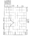
FIG. 2 is a schematic diagram showing the measured working bandwidth of an antenna structure of one embodiment of the invention.
DETAILED DESCRIPTION OF THE EMBODIMENTS
As shown in FIG. 1, an antenna structure 100 of one embodiment of the invention is a circuit board antenna, and it can be applied to any electronic device and a 2.4 GHz wireless local area network (WLAN), a Bluetooth system or a radio frequency identification (RFID) system.
The antenna structure 100 includes a circuit board 110 and a printed antenna 120 printed on the circuit board 110 in a single layer or multilayer mode. In the embodiment, the thickness of the circuit board 110 is 0.81 mm, and the circuit board 110 has a ground surface G.
The printed antenna 120 includes a signal feed-in portion 121, a first radiating unit 122, a second radiating unit 123 and a ground portion 124. The signal feed-in portion 121, the first radiating unit 122 and the ground portion 124 is printed on the circuit board 110 in a single layer mode. The second radiating unit 123 is printed on the circuit board 110 in a multilayer mode. The signal feed-in portion 121 is used for receiving or transmitting a signal received or transmitted by the first radiating unit 122 and the second radiating unit 123. The transmission path of the signal is denoted by arrows shown in FIG. 1 (only one direction of the signal transmission path is shown in FIG. 1, but the embodiment is not limited by this).
The signal feed-in portion 121 has a first end E1. The first radiating unit 122 diverges and forms a first radiating element 1221 and a second radiating element 1222 at the first end E1. The first radiating element 1221 and the second radiating element 1222 are combined at a second end E2. The first radiating element 1221 has a first turning portion T1, the second radiating element 1222 is connected to the ground portion 124. Then the printed antenna can be connected to the ground surface G via the ground portion 124 to be connected to ground.
The second radiating unit 123 is a multiplayer printed unit, and it includes a third radiating element 1231, a fourth radiating element 1232, a second turning portion T2 and a third turning portion T3. The second radiating unit 123 is connected to the first radiating unit 122 via the third radiating element 1231. The second turning portion T2 is located between the third radiating element 1231 and the first radiating unit 122, and the third turning portion T3 is located between the third radiating element 1231 and the fourth radiating element 1232. A distance d is formed between the fourth radiating element 1232 and the ground surface G to generate a parasitic capacitance.
The signal is sent by the signal feed-in portion 121. When the signal is transmitted through the first radiating unit 122, the signal can be selectively transmitted through the first radiating element 1221 and the first turning portion T1 or through the second radiating element 1222 to enter the second radiating unit 123. Then, the signal enters the third radiating element 1231 through the second turning portion T2 and further enters the fourth radiating element 1232 through the third turning portion T3. The first turning portion T1, the second turning portion T2 and the third turning portion T3 have forty-five degree angles with the incident direction of the signal, and then the signal can be rapidly transmitted.
The printed antenna 120 of the embodiment of the invention occupies an area of the circuit board, and the size of the area is about 71.96 mm2. The ratio of the length D1 of the area to the width D2 of the area is about 1.7:1. Ratios of the distance d between the fourth radiating element 1232 and the ground surface G to the length D1 and the width D2 of the area are about 1:14 and about 1:8, respectively.
As shown in FIG. 2, FIG. 2 is a schematic diagram showing measured S11 data of an antenna according to a preferred embodiment of the invention. The usable bandwidth of antennas are generally required to satisfy S11<−10 dB (or voltage standing wave ratio (VSWR) <1.92; the two parameters have the same meaning and can be derived from each other). In FIG. 2, S11 is −11.04 dB and the frequency is 2.35 GHz at point 1 (▾), and S11 is −10.75 dB and the frequency is 2.52 GHz at point 3(∇). A bandwidth between the frequency 2.35 GHz and the frequency 2.52 GHz is 0.17 GHz, and S11 is less than −10 dB, so that the bandwidth is a usable bandwidth which is 170 MHz. The printed antenna 120 of the embodiment of the invention occupies a small area, but its radiation efficiency is above seventy percent, and the usable bandwidth reaches 170 MHz.
From the above, the antenna structure 100 of the preferred embodiment of the invention has a tiny volume, and the printed antenna can be directly printed on the circuit board 110. Compared with a conventional multilayer ceramic antenna, the cost of the antenna structure of the invention is low, and the working bandwidth and the radiation efficiency of the antenna structure of the invention are greatly increased.
Although the present invention has been described in considerable detail with reference to certain preferred embodiments thereof, the disclosure is not for limiting the scope of the invention. Persons having ordinary skill in the art may make various modifications and changes without departing from the scope and spirit of the invention. Therefore, the scope of the appended claims should not be limited to the description of the preferred embodiments described above.

Claims (9)

1. An antenna structure comprising:
a circuit board having a ground surface; and
a printed antenna arranged on the circuit board comprising:
a signal feed-in portion;
a first radiating unit connected to the signal feed-in portion and having a first end and a second end, wherein the first radiating unit diverges and forms a first radiating element and a second radiating element at the first end, the first radiating element and the second radiating element are combined at the second end, and the first radiating element has a first turning portion; and
a second radiating unit connected to the first radiating unit, and having a plurality of printed layers, a third radiating element, a fourth radiating element, a second turning portion and a third turning portion, wherein the second turning portion is located between the third radiating element and the second end, the third turning portion is located between the third radiating element and the fourth radiating element, and a distance is formed between the fourth radiating element and the ground surface.
2. The antenna structure according to claim 1, wherein the printed antenna occupies an area of the circuit board, and the ratio of the length of the area to the width of the area is about 1.7:1.
3. The antenna structure according to claim 2, wherein the ratio of the distance to one length of the area is about 1:14.
4. The antenna structure according to claim 2, wherein the ratio of the distance to one width of the area is about 1:8.
5. The antenna structure according to claim 1, wherein the printed antenna further comprises a ground portion connected to the first radiating unit.
6. The antenna structure according to claim 1, wherein the printed antenna further comprises a ground portion connected to the second radiating unit.
7. The antenna structure according to claim 1, wherein the signal feed-in portion receives or transmits a signal, and the first turning portion, the second turning portion and the third turning portion have forty-five degree angles with the incidence direction of the signal.
8. The antenna structure according to claim 1, wherein the signal enters from the feed-in portion and is selectively transmitted through the first radiating element or the second radiating element of the first radiating unit to enter the second radiating unit.
9. The antenna structure according to claim 1, wherein the distance between the fourth radiating element and the ground surface is suitable to generate a parasitic capacitance.
US12/183,014 2007-08-24 2008-07-30 Antenna structure Active 2029-02-04 US7773036B2 (en)

Priority Applications (1)

Application Number Priority Date Filing Date Title
US12/834,812 US7961149B2 (en) 2007-08-24 2010-07-12 Antenna structure

Applications Claiming Priority (3)

Application Number Priority Date Filing Date Title
TWTW96131466 2007-08-24
TW96131466A 2007-08-24
TW096131466A TWI338412B (en) 2007-08-24 2007-08-24 Antenna structure

Related Child Applications (1)

Application Number Title Priority Date Filing Date
US12/834,812 Continuation US7961149B2 (en) 2007-08-24 2010-07-12 Antenna structure

Publications (2)

Publication Number Publication Date
US20090051600A1 US20090051600A1 (en) 2009-02-26
US7773036B2 true US7773036B2 (en) 2010-08-10

Family

ID=40134356

Family Applications (2)

Application Number Title Priority Date Filing Date
US12/183,014 Active 2029-02-04 US7773036B2 (en) 2007-08-24 2008-07-30 Antenna structure
US12/834,812 Active US7961149B2 (en) 2007-08-24 2010-07-12 Antenna structure

Family Applications After (1)

Application Number Title Priority Date Filing Date
US12/834,812 Active US7961149B2 (en) 2007-08-24 2010-07-12 Antenna structure

Country Status (3)

Country Link
US (2) US7773036B2 (en)
EP (1) EP2028716B1 (en)
TW (1) TWI338412B (en)

Families Citing this family (1)

* Cited by examiner, † Cited by third party
Publication number Priority date Publication date Assignee Title
CN111969323B (en) * 2019-05-20 2023-02-28 中兴通讯股份有限公司 Antenna system and terminal

Citations (9)

* Cited by examiner, † Cited by third party
Publication number Priority date Publication date Assignee Title
JP2004096314A (en) 2002-08-30 2004-03-25 Taiyo Yuden Co Ltd Dielectric antenna and mobile communication apparatus with built-in the same
US20040201528A1 (en) 2003-04-08 2004-10-14 Yageo Corporation Integrated antenna for portable computer
US20040246188A1 (en) 2003-06-09 2004-12-09 Houkou Electric Co., Ltd. Multi-frequency antenna and constituting method thereof
US6853335B1 (en) * 2003-08-21 2005-02-08 D-Link Corporation Miniature monopole antenna for dual-frequency printed circuit board
CN2682470Y (en) 2004-04-05 2005-03-02 英业达股份有限公司 Notebook computer with printed circuit board antenna
US6956530B2 (en) * 2002-09-20 2005-10-18 Centurion Wireless Technologies, Inc. Compact, low profile, single feed, multi-band, printed antenna
CN1913224A (en) 2005-08-09 2007-02-14 技嘉科技股份有限公司 Circuit board antenna
JP2007088975A (en) 2005-09-26 2007-04-05 Toshiba Corp Wireless device
US7541980B2 (en) * 2006-04-14 2009-06-02 Hon Hai Precision Industry Co., Ltd. Printed antenna

Family Cites Families (1)

* Cited by examiner, † Cited by third party
Publication number Priority date Publication date Assignee Title
KR100530667B1 (en) * 2003-11-20 2005-11-22 주식회사 팬택 Internal antenna for mobile handset

Patent Citations (9)

* Cited by examiner, † Cited by third party
Publication number Priority date Publication date Assignee Title
JP2004096314A (en) 2002-08-30 2004-03-25 Taiyo Yuden Co Ltd Dielectric antenna and mobile communication apparatus with built-in the same
US6956530B2 (en) * 2002-09-20 2005-10-18 Centurion Wireless Technologies, Inc. Compact, low profile, single feed, multi-band, printed antenna
US20040201528A1 (en) 2003-04-08 2004-10-14 Yageo Corporation Integrated antenna for portable computer
US20040246188A1 (en) 2003-06-09 2004-12-09 Houkou Electric Co., Ltd. Multi-frequency antenna and constituting method thereof
US6853335B1 (en) * 2003-08-21 2005-02-08 D-Link Corporation Miniature monopole antenna for dual-frequency printed circuit board
CN2682470Y (en) 2004-04-05 2005-03-02 英业达股份有限公司 Notebook computer with printed circuit board antenna
CN1913224A (en) 2005-08-09 2007-02-14 技嘉科技股份有限公司 Circuit board antenna
JP2007088975A (en) 2005-09-26 2007-04-05 Toshiba Corp Wireless device
US7541980B2 (en) * 2006-04-14 2009-06-02 Hon Hai Precision Industry Co., Ltd. Printed antenna

Also Published As

Publication number Publication date
TWI338412B (en) 2011-03-01
US20090051600A1 (en) 2009-02-26
US7961149B2 (en) 2011-06-14
US20100277391A1 (en) 2010-11-04
EP2028716B1 (en) 2017-04-05
TW200910685A (en) 2009-03-01
EP2028716A1 (en) 2009-02-25

Similar Documents

Publication Publication Date Title
US7385556B2 (en) Planar antenna
US6747600B2 (en) Dual-band monopole antenna
US7102586B2 (en) Antenna and antenna array
US6650296B2 (en) Dual-band monopole antenna
US20100073238A1 (en) Microstrip patch antenna with high gain and wide band characteristics
US20040189530A1 (en) Dual frequency band inverted-F antenna
US20050140551A1 (en) High performance low cost monopole antenna for wireless applications
US20100123631A1 (en) Multi-band Antenna for a Wireless Communication Device
US8432313B2 (en) Conformal and compact wideband antenna
JP2002076735A (en) Pattern antenna and radio communication equipment using the same
JP2001326521A (en) Laminated pattern antenna, and radio communication equipment provided with the same
US8022881B2 (en) Multiband antenna
US9136604B2 (en) Antenna and wireless communication apparatus
US20120262342A1 (en) Multiband antenna
JP2011035440A (en) Antenna, and communication device including the same
KR100980779B1 (en) Apparatus of Chip Antenna For Ultra-Wide-Band Applications
CN101895009A (en) Double-frequency broad-band antenna with symmetrical dipole-tapered slot line combined structure
US8063830B2 (en) Antenna device
CN103427154B (en) High efficiency antenna
US20110037659A1 (en) Antenna apparatus
US7773036B2 (en) Antenna structure
JP2007312004A (en) Antenna system
US9431710B2 (en) Printed wide band monopole antenna module
US7872606B1 (en) Compact ultra wideband microstrip resonating antenna
JP2008172602A (en) Antenna unit

Legal Events

Date Code Title Description
AS Assignment

Owner name: ASUSTEK COMPUTER INC., TAIWAN

Free format text: ASSIGNMENT OF ASSIGNORS INTEREST;ASSIGNOR:TSAI, HSIAO-MING;REEL/FRAME:021346/0840

Effective date: 20080716

STCF Information on status: patent grant

Free format text: PATENTED CASE

FPAY Fee payment

Year of fee payment: 4

MAFP Maintenance fee payment

Free format text: PAYMENT OF MAINTENANCE FEE, 8TH YEAR, LARGE ENTITY (ORIGINAL EVENT CODE: M1552)

Year of fee payment: 8

MAFP Maintenance fee payment

Free format text: PAYMENT OF MAINTENANCE FEE, 12TH YEAR, LARGE ENTITY (ORIGINAL EVENT CODE: M1553); ENTITY STATUS OF PATENT OWNER: LARGE ENTITY

Year of fee payment: 12