BACKGROUND OF THE INVENTION
1. Field of the Invention
The present invention relates to a pulse width modulation circuit and related method, and more particularly, to a pulse width modulation circuit capable of linearly adjusting duty cycle with voltage and related method.
2. Description of the Prior Art
Pulse width modulation (PWM) technique is widely used for output power control, such as power management, motor control, audio amplifiers, etc. Please refer to FIG. 1, which illustrates a schematic diagram of a PWM circuit 10 in the prior art. The PWM circuit 10 includes a reference voltage generator 102, a triangular wave oscillator 104, and a comparator 106. The PWM circuit 10 is utilized for outputting a PWM signal SPWM with periodic variation of pulse width according to a result of comparing a reference voltage VR with a periodic triangular wave (or a sawtooth wave) signal VT. The prior art can control the output power by changing duty cycle of the PWM signal SPWM. Taking the U.S. patent publication document (patent publication NO. 2005/0269985) as an example, the PWM circuit 10 has a periodic triangular wave (or sawtooth wave) signal VT with fixed high and low voltage levels. As the reference voltage VR generated by the reference voltage generator 102 is linearly proportional to the input DC voltage Vin, the duty cycle of the PWM signal SPWM is linearly varied with the input DC voltage Vin. To make short of the matter, the duty cycle of the PWM signal SPWM can be linearly tunable by voltage levels of the input DC voltage Vin.
This method has some limitations and can't meet some application requirements, especially for the cases of tuning wider range of duty cycle. Modifying the design of the reference voltage generator 102 should be a solution, but it takes much more components. Another approach is to control the high and low voltage levels of the triangular wave signal VT via the input DC voltage Vin. It should be noted that the reference voltage VR is fixed for this case. In this way, the input DC voltage Vin can adjust duty cycle of the PWM signal SPWM across a wider range. However, the relation between the duty cycle of the pulse width modulation signal SPWM and the input DC voltage Vin, as shown in FIG. 2, can not achieve absolutely linearity. This nonlinear relationship should contribute some unwanted influences. For example, when a PWM signal SPWM is utilized for speed control of a fan motor, it may result in a non-linear relation between the input DC voltage Vin and the speed.
SUMMARY OF THE INVENTION
The primary objective of the present invention is to provide a pulse width modulation circuit capable of linearly adjusting duty cycle with voltage and related method.
The present invention discloses a pulse width modulation circuit capable of linearly adjusting duty cycle with voltage, which comprises an input voltage source for generating an input voltage, a regulator coupled to the input voltage source for generating a regulated voltage, a first voltage-dividing unit coupled to the regulator and a ground terminal for providing a first divided voltage, a second voltage-dividing unit coupled to the regulator and the ground terminal for providing a second divided voltage, a third voltage-dividing unit coupled to the input voltage source and the ground terminal for providing a third divided voltage, a voltage adder coupled to the a first voltage-dividing unit and the third voltage-dividing unit for adding the first divided voltage and the third divided voltage for generating a high level voltage, a waveform generator coupled to the voltage adder and the third voltage-dividing unit for generating an oscillating signal according to the high level voltage and the third divided voltage, and a comparator having a first input terminal coupled to the second voltage-dividing unit, a second terminal coupled to the waveform generator, and an output terminal for comparing the second divided voltage with the oscillating signal to output a pulse width modulation signal through the output terminal.
The present invention further discloses a method capable of linearly adjusting duty cycle with voltage for a pulse width modulation circuit, which the method comprises generating a regulated voltage according to an input voltage; transforming the regulated voltage into a first divided voltage and a second divided voltage, and transforming the input voltage into a third divided voltage; adding the first divided voltage and the third divided voltage for generating a high level voltage; generating an oscillating signal according to the high level voltage and the third divided voltage; and comparing the second divided voltage with the oscillating signal to output a pulse width modulation signal.
These and other objectives of the present invention will no doubt become obvious to those of ordinary skill in the art after reading the following detailed description of the preferred embodiment that is illustrated in the various figures and drawings.
BRIEF DESCRIPTION OF THE DRAWINGS
FIG. 1 is a schematic diagram of a PWM circuit in the prior art.
FIG. 2 is a schematic diagram showing the relationship between duty cycle of the PWM signal and input DC voltage in the modified prior art for wider tuning range of duty cycle.
FIG. 3 is a schematic diagram of a pulse width modulation circuit according to an embodiment of the invention.
FIG. 4 is a schematic diagram of waveforms showing generation of a pulse width modulation signal according to an embodiment of the invention.
FIG. 5 is a schematic diagram showing waveforms of the pulse width modulation signal under various input voltage values according to an embodiment of the invention.
FIG. 6 is a schematic diagram showing the relationship between the duty cycle of the pulse width modulation signal and the input voltage according to an embodiment of the invention.
FIG. 7 is a schematic diagram of a procedure according to an embodiment of the present invention.
DETAILED DESCRIPTION
FIG. 3 is a schematic diagram of a pulse width modulation circuit 30 according to an embodiment of the invention. The pulse width modulation circuit 30 utilized for adjusting duty cycle according an input voltage includes an input voltage source P, a regulator 302, a first voltage-dividing unit 304, a second voltage-dividing unit 306, a third voltage-dividing unit 308, a voltage adder 310, a waveform generator 312, and a comparator 314. The input voltage source P is utilized for generating an input voltage VCC. The regulator 302 is coupled to input voltage source P for generating a regulated voltage VREG. The first voltage-dividing unit 304 is coupled to regulator 302 and a ground terminal for providing a first divided voltage V1. The second voltage-dividing unit 306 is coupled to regulator 302 and the ground terminal for providing a second divided voltage V2. The third voltage-dividing unit 308 is coupled to input voltage source P and the ground terminal for providing a third divided voltage V3. The voltage adder 310 is coupled to first voltage-dividing unit 304 and third voltage-dividing unit 308 for adding the first divided voltage V1 and the third divided voltage V3 to generate a high level voltage VH. The waveform generator 312 is coupled to voltage adder 310 and third voltage-dividing unit 308 for generating an oscillating signal OSC with high and low voltage levels are VH and V3, respectively. The comparator 314 is coupled to second voltage-dividing unit 306 and waveform generator 312 for comparing the second divided voltage V2 with the oscillating signal OSC to output a pulse width modulation signal SPWM, so as to control driving component directly.
As illustrated in FIG. 3, the first voltage-dividing unit 304 includes a first voltage-dividing output terminal O1, a first voltage-dividing resistor R1, and a second voltage dividing resistor R2. The first voltage-dividing output terminal O1 is coupled to the voltage adder 310 and V1 is the divided output voltage. The first voltage dividing resistor R1 is coupled between the regulator 302 and the first voltage-dividing output terminal O1. The second voltage dividing resistor R2 is coupled between the first voltage-dividing output terminal O1 and the ground terminal. The second voltage-dividing unit 306 includes a second voltage-dividing output terminal O2, a third voltage dividing resistor R3, and a fourth voltage dividing resistor R4. The second voltage-dividing output terminal O2 is coupled to a first input terminal of comparator 314 and V2 is the divided output voltage. The third voltage-dividing resistor R3 is coupled between the regulator 302 and the second voltage-dividing output terminal O2. The fourth voltage-dividing resistor R4 is coupled between the second voltage-dividing output terminal O2 and the ground terminal. The third voltage-dividing unit 308 includes a third voltage-dividing output terminal O3, a fifth voltage dividing resistor R5, and a sixth voltage dividing resistor R6. The third voltage-dividing output terminal O3 is coupled to voltage adder 310 and waveform generator 312 and V3 is the divided output voltage. The fifth voltage-dividing resistor R5 is coupled between the input voltage source P and the third voltage-dividing output terminal O3. The sixth voltage-dividing resistor R6 is coupled between the third voltage-dividing output terminal O3 and the ground terminal.
FIG. 4 is a schematic diagram of waveforms showing generation of a pulse width modulation signal SPWM according to an embodiment of the invention. In the pulse width modulation circuit 30, the input voltage VCC generated by the input voltage source P can be considered as an external control voltage source. In addition, the regulator 302 can provide and maintain a stable DC voltage level, VREG, which should not change with variation of load current and input voltage. Note the specification for output value of a regulator should be set within a default value. The voltage adder 310 adds the first divided voltage V1 and the third divided voltage V3 to generate a high level voltage VH (i.e. VH=V1+V3). The waveform generator 312 generates an oscillating signal OSC according to high level voltage VH and the third divided voltage V3. The signal OSC could be a triangular or sawtooth waveform and it's high and low voltage levels would be VH and V3, respectively. The amplitude of the oscillating signal OSC is equal to the first divided voltage V1. The comparator 314 compares the second divided voltage V2 with the oscillating signal OSC to generate a pulse width modulation signal SPWM. The duty cycle of the pulse width modulation signal SPWM can be determined as follows:
The high and low levels' relationship of the oscillating signal OSC generated by the waveform generator 312 can be expressed as follows:
VH=V1+V3 (2)
By substituting the equation (2) into the equation (1), the following equation is obtained:
where VCC is the input voltage, and the Ka is the ratio of voltage dividing resistors for V3
The first divided voltage V1 and the second divided voltage V2 are derived from the regulated voltage VREG. The ratio of voltage-dividing resistors for V3 is Ka. One can get that V1, V2, and Ka are independent to the input voltage VCC. From the equation (3), it can be appreciated that the duty cycle is linearly proportional to the input voltage VCC. The slope of equation (3) is determined by the first divided voltage V1 and Ka, the ratio of voltage dividing resistors. The values of this slope can be adjusted flexibly by setting the first divided voltage V1 and the ratio of voltage dividing resistors Ka to meet various requirements of duty cycle control. Similarly, the desired duty cycle of the pulse width modulation signal SPWM can also be linear adjusted by setting the second divided voltage V2.
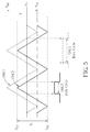
FIG. 5 illustrates the waveforms of the pulse width modulation signal under various input voltage values according to an embodiment of the invention. Suppose that two input voltage levels VCC1 and VCC2 are applied in the pulse width modulation circuit 30 respectively. And the voltage level of VCC1 is higher than that of VCC2. When the input voltage level VCC1 is applied as the input voltage, OSC1 indicates the oscillating signal, VH1 indicates the high level of the oscillating signal OSC1, and V31 indicates the low level of the oscillating signal OSC1. Similarly, when the other input voltage level VCC2 is applied as the input voltage, OSC2 indicates the oscillating signal, VH2 indicates the high level of the oscillating signal OSC2, and V32 indicates the low level of the oscillating signal OSC2. The pulse width modulation signals SPWM1 and SPWM2 corresponding to the VCC1 and VCC2 are outputted from the comparator 314 respectively. Please note that both conditions have the same amplitude V1 for the oscillating signal and the same reference voltage V2. It can be seen that the higher the input voltage level VCC is, the larger the duty cycle is.
FIG. 6 shows the relationship between the duty cycle of the pulse width modulation signal SPWM and the input voltage VCC according to an embodiment of the invention. Under various settings of first divided voltage V1 (i.e. various amplitudes), the input voltage is linearly proportional to the duty cycle. As a result, the pulse width modulation circuit 30 of the present invention is capable of improving the applications of pulse width modulation effectively. For the example of utilizing the pulse width modulation circuit 30 in speed control of a fan motor, one can linearly adjust the speed of the fan motor because of the duty cycle of the pulse width modulation signal SPWM linearly changed by the input voltage VCC.
Therefore, through the pulse width modulation circuit 30 of the present invention, the duty cycle of the pulse width modulation signal SPWM has linear relation with the input voltage VCC, and the voltage levels of the oscillating signal OSC can be controlled via external input voltage, so as to linearly control the duty cycle of the pulse width modulation signal SPWM. The desired linear slope values can also be adjusted flexibly for conforming to various application requirements of the duty cycle control without additional complicated components. In other words, the present invention is capable of linearly adjusting the duty cycle of the pulse width modulation signal with input voltage and flexibility providing variations for various duty cycles.
Please note that the pulse width modulation circuit 30, shown in FIG. 3, is a schematic diagram according to an exemplary embodiment of the present invention. Those skilled in the art can make alternations and modifications accordingly. For example, first voltage-dividing unit 304, second voltage-dividing unit 306, and third voltage-dividing unit 308 can provide any desired divided voltage value by dividing the regulated voltage or input voltage with resistors or other devices. These should not be a limitation of the present invention. The waveform generator 312 can be utilized for generating all kinds of oscillating signals, such as triangular wave signals, saw tooth wave signals, ramp signals, etc. In addition, the duty cycle of the pulse width modulation signal cannot only be adjusted by setting the input voltage VCC, but also by setting the first divided voltage V1 or the second divided voltage V2.
As to the operation of the pulse width modulation circuit 30, please refer to FIG. 7. FIG. 7 is a schematic diagram of a procedure 70 according to an embodiment of the present invention. The procedure 70 is capable of being the operating procedure for the pulse width modulation circuit 30. The procedure 70 comprises the following steps:
Step 700: Start.
Step 702: Generate a regulated voltage VREG according to an input voltage VCC.
Step 704: Transform the regulated voltage VREG into a first divided voltage V1 and a second divided voltage V2, and transform input voltage VCC into a third divided voltage V3.
Step 706: Add the first divided voltage V1 and the third divided voltage V3 for generating a high level voltage VH.
Step 708: Generate an oscillating signal OSC according to high level voltage VH and the third divided voltage V3.
Step 710: Compare second divided voltage V2 with oscillating signal OSC to output a pulse width modulation signal SPWM.
Step 712: End.
According to the procedure 70, the present invention generates the regulated voltage VREG according to input voltage VCC. After that, the regulated voltage VREG can be transformed into a first divided voltage V1 and a second divided voltage V2, and the input voltage VCC can be transformed into a third divided voltage V3. Furthermore, the voltage adder 310 adds first divided voltage V1 and the third divided voltage V3 to generate a high level voltage VH. The waveform generator 312 is capable of generating an oscillating signal OSC according to high level voltage VH and the third divided voltage V3. Finally, the comparator 314 compares second divided voltage V2 with oscillating signal OSC so as to output a pulse width modulation signal SPWM. The procedure 70 is utilized for illustrating the operation method of the pulse width modulation circuit 30. The related variations and the detailed description that referred to the foregoing illustration are omitted herein.
In summary, through the pulse width modulation circuit 30 of the present invention, the duty cycle of the pulse width modulation signal SPWM has linear relation with the input voltage VCC. The voltage levels of the oscillating signal OSC can be controlled via external input voltage, VCC, so as to linearly control the duty cycle of the pulse width modulation signal SPWM. Furthermore, the desired linear slope values can also be adjusted flexibly for conforming to various variations of the duty cycle control requirements without additional complicated components.
Those skilled in the art will readily observe that numerous modifications and alterations of the device and method may be made while retaining the teachings of the invention.