US7764057B2 - Constant-on-time switching power supply with virtual ripple feedback and related system and method - Google Patents
Constant-on-time switching power supply with virtual ripple feedback and related system and method Download PDFInfo
- Publication number
- US7764057B2 US7764057B2 US11/087,323 US8732305A US7764057B2 US 7764057 B2 US7764057 B2 US 7764057B2 US 8732305 A US8732305 A US 8732305A US 7764057 B2 US7764057 B2 US 7764057B2
- Authority
- US
- United States
- Prior art keywords
- voltage
- threshold
- threshold voltage
- switch
- response
- Prior art date
- Legal status (The legal status is an assumption and is not a legal conclusion. Google has not performed a legal analysis and makes no representation as to the accuracy of the status listed.)
- Active, expires
Links
Images


Classifications
-
- H—ELECTRICITY
- H02—GENERATION; CONVERSION OR DISTRIBUTION OF ELECTRIC POWER
- H02M—APPARATUS FOR CONVERSION BETWEEN AC AND AC, BETWEEN AC AND DC, OR BETWEEN DC AND DC, AND FOR USE WITH MAINS OR SIMILAR POWER SUPPLY SYSTEMS; CONVERSION OF DC OR AC INPUT POWER INTO SURGE OUTPUT POWER; CONTROL OR REGULATION THEREOF
- H02M3/00—Conversion of dc power input into dc power output
- H02M3/02—Conversion of dc power input into dc power output without intermediate conversion into ac
- H02M3/04—Conversion of dc power input into dc power output without intermediate conversion into ac by static converters
- H02M3/10—Conversion of dc power input into dc power output without intermediate conversion into ac by static converters using discharge tubes with control electrode or semiconductor devices with control electrode
- H02M3/145—Conversion of dc power input into dc power output without intermediate conversion into ac by static converters using discharge tubes with control electrode or semiconductor devices with control electrode using devices of a triode or transistor type requiring continuous application of a control signal
- H02M3/155—Conversion of dc power input into dc power output without intermediate conversion into ac by static converters using discharge tubes with control electrode or semiconductor devices with control electrode using devices of a triode or transistor type requiring continuous application of a control signal using semiconductor devices only
- H02M3/156—Conversion of dc power input into dc power output without intermediate conversion into ac by static converters using discharge tubes with control electrode or semiconductor devices with control electrode using devices of a triode or transistor type requiring continuous application of a control signal using semiconductor devices only with automatic control of output voltage or current, e.g. switching regulators
-
- H—ELECTRICITY
- H02—GENERATION; CONVERSION OR DISTRIBUTION OF ELECTRIC POWER
- H02M—APPARATUS FOR CONVERSION BETWEEN AC AND AC, BETWEEN AC AND DC, OR BETWEEN DC AND DC, AND FOR USE WITH MAINS OR SIMILAR POWER SUPPLY SYSTEMS; CONVERSION OF DC OR AC INPUT POWER INTO SURGE OUTPUT POWER; CONTROL OR REGULATION THEREOF
- H02M1/00—Details of apparatus for conversion
- H02M1/0003—Details of control, feedback or regulation circuits
- H02M1/0025—Arrangements for modifying reference values, feedback values or error values in the control loop of a converter
Definitions
- a switching power supply provides a high-efficiency regulated output voltage for a variety of power-management functions that are often required in modern electronic systems. These systems have either a battery or an unregulated power supply as their input power sources, and may have multiple power output voltages that require power conversion, power management functions, and tight regulation.
- the function of a switching power supply is to convert power from an input power source to output power for an electronic system. This conversion should be at high efficiency for the various operational modes of the system. For example, when a notebook computer or cellular phone system is operated in a low-power mode, it is desired to extend battery life. On the other hand, a well-regulated voltage supply is desired when the notebook or phone is operated in a high-power mode. Furthermore, the switching power supply is required to respond with little or no regulation error when the notebook or phone changes from a low- to a high-power mode.
- a switching power supply provides a regulated output voltage by controlling a supply current through a power switching stage.
- the switched current is connected to a filter stage, which reduces the resulting ripple voltage.
- a feedback stage measures the regulated output voltage and, in response to the measured value of the regulated output voltage, generates a control signal that controls the power switching stage.
- the control signal activates the power switching stage when the regulated output voltage drops below a threshold voltage (for a positive regulated output voltage) and then deactivates the switching power stage when the regulated output voltage increases above the threshold voltage.
- the pulse width of the control signal determines the period of time that the power switching stage provides current to the filter stage, and hence, the supply regulates the output voltage by controlling the widths of the control-signal pulses. Therefore, the pulse width of the control signal is proportional to the current being drawn by the load, and the frequency of the control signal is typically constant.
- the control signal activates the power switching stage for a predetermined constant time when the regulated output voltage drops below a threshold voltage (for a positive voltage). Therefore, the pulse width of the control signal is constant, and the frequency of the control signal is proportional to the current drawn by the load.
- the supply operates at a constant switching frequency without a synchronizing signal. But in noisy environments, noise may be superimposed on the output voltage or threshold voltage, and this noise may cause jitter in the phase, and thus the frequency, of the control signal. Unfortunately, this jitter may cause the power supply to irradiate electromagnetic interference that can adversely affect the electronic system that incorporates the power supply or nearby electronic systems.
- An embodiment of the invention is a signal regulator that includes a switching circuit, a controller, and a threshold generator.
- the switching circuit generates an output voltage regulated by the controller, which regulates the output voltage by, activating the switching circuit for a predetermined time when the output voltage has a predetermined relationship to a threshold voltage.
- the threshold generator generates the threshold voltage in response to the controller.
- the threshold circuit may generate the threshold voltage as the sum of a base voltage and a virtual ripple voltage.
- the virtual ripple voltage decreases the effect that noise has on jitter by increasing the signal-to-noise ratio.
- the output equivalent-series-resistance (ESR) voltage ramp combines with the virtual ripple signal to create a total signal that compares to the threshold voltage. Increasing the total signal acts to reduce the magnitude of noise-induced jitter.
- FIG. 1 is a schematic block diagram of a constant-on-time switching power supply with virtual ripple feedback according to an embodiment of the invention.
- FIGS. 2A-2C are timing diagrams of some of the signals that the power supply of FIG. 1 generates according to an embodiment of the invention.
- FIG. 3 is a schematic block diagram of a constant-on-time switching power supply with virtual ripple feedback according to another embodiment of the invention.
- FIGS. 4A-4C are timing diagrams of some of the signals that the power supply of FIG. 3 generates according to an embodiment of the invention.
- FIG. 5 is a detailed schematic diagram of the power supply of FIG. 1 according to an embodiment of the invention.
- FIG. 6 is a schematic block diagram of a computer system that can incorporate the power supplies of FIGS. 1 and 4 according to an embodiment of the invention.
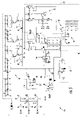
- FIG. 1 is a schematic block diagram of a constant-on-time buck-converter power supply 10 , which uses virtual ripple feedback and which provides a regulated voltage Vout to a load 12 according to an embodiment of the invention.
- the supply 10 includes a filter 14 , a switching circuit 16 , and a regulator 18 .
- Vout is a positive voltage, although a similar discussion applies where Vout is negative.
- the filter 14 includes an inductor L and a capacitor C
- the switching circuit 16 includes NMOS power transistors 20 a and 20 b , which have their source and drain, respectively, coupled to the inductor L.
- the drain of the transistor 20 a is coupled to Vin, which is the supply voltage (possibly unregulated) from which the supply 10 generates Vout. Because the supply 10 is a buck step-down converter, Vin is higher than Vout. Vin may also be coupled to the regulator 18 as discussed below.
- the regulator 18 includes a switching controller 22 and a threshold-signal generator 24 .
- the controller 22 includes a comparator 26 for comparing Vout to the threshold signal, which is a voltage Vthresh in this embodiment, and includes conventional switching logic 28 for activating the transistor 20 a for a predetermined constant time in response to Vthresh being greater than Vout.
- the circuit 34 may also be coupled to Vref and Vout as discussed below. Furthermore, Vref may be derived from a band-gap reference generator, or generated in any other suitable manner.
- FIG. 2A is a timing diagram of Vout as generated by the power supply 10 ( FIG. 1 ) during steady-state operation of the load 12 according to an embodiment of the invention.
- the power supply 10 generates Vout so that it does not fall below Vref Therefore, the average level of Vout under ideal steady-state conditions equals Vref+A/2, where A is the peak-to-peak ripple amplitude, which is typically on the order of a few millivolts (mV).
- FIG. 2B is a timing diagram of Vthresh according to an embodiment of the invention where Voffset is negative.
- the ramp circuit 30 generates IRamp so as to generate Vthresh (at the node 32 ) as a saw-tooth wave having a base voltage equal to Vref ⁇ Voffset and a peak-to-peak voltage on the order of a few millivolts. Therefore, Vthresh is a virtual ripple voltage that is superimposed on the base voltage. Furthermore, Vthresh is generated in response to switching-state feedback from the controller 22 , and optional feedback from Vout (dashed line to the offset circuit 34 ).
- FIG. 2C is a timing diagram of Vthresh and Vout according to an embodiment of the invention. Because of the saw-tooth shape of Vthresh and the ripple on Vout, the difference between Vout and Vthresh is relatively large except when Vout and Vthresh simultaneously “meet” at Vref. This difference significantly increases the noise margin compared to conventional techniques such as where Vthresh merely equals Vref.
- Vin is not coupled to the regulator 22 and neither Vref nor Vout is coupled to the offset circuit 34 .
- the switching logic 28 deactivates the transistor 20 b and activates the transistor 20 a , thus causing a charging current to flow from Vin, through the inductor L, to the filter capacitor C and to the load 12 —ideally, the rising Vthresh and falling Vout “meet” at Vref, such that Vout becomes less than Vref at the same time that it becomes less than Vthresh.
- This charging current causes Vout to rise. Assuming that in a steady state the load 12 draws a constant current, the actual rate of this rise depends on the capacitance and equivalent series resistance (ESR) of C.
- ESR equivalent series resistance
- the capacitance and ESR of C are sufficiently large such that Vout increases at a substantially constant rate (i.e., straight line) as shown.
- the switching logic 23 In response to activating the transistor 20 a , the switching logic 23 generates a DISABLE signal, which causes the threshold-signal generator 24 to “discharge” the node 32 to the base voltage of Vref ⁇ Voffset.
- the switching logic 23 deactivates the transistor 20 a and activates the transistor 20 b , thus allowing the current stored in the inductor L to continue flowing. As this current decays, Vout falls. When Vout falls below Vthresh, the above-described cycle is repeated.
- the switching logic 23 in response to deactivating the transistor 20 a , the switching logic 23 generates a TURN-ON SYNC signal, which causes the ramp generator 30 to generate IRamp, and thus causes the threshold-signal generator 24 to ramp Vthreshold upward from the base voltage Vref ⁇ Voffset at a predetermined rate.
- Vthresh rises above Vout, the above-described cycle is repeated. If one knows the steady-state current drawn by the load 12 , then he can calculate the steady-state ripple of Vout, and set Voffset and the slope of the Vthresh ramp such that during steady-state operation of the load, Voffset and Vout “meet” at Vref as is desired.
- the minimum level of Vout may be less than or greater than Vref.
- the ripple amplitude A increases, and Vthresh and Vout “meet” at a voltage less than Vref.
- the ripple amplitude A decreases, and Vthresh and Vout “meet” at a voltage greater than Vref.
- the comparator 26 compares Vout to Vthresh instead of to the constant Vref, the noise margin is often increased, and thus jitter in the switching frequency, and the undesirable affects of such jitter, are often reduced.
- the offset circuit 34 can receive Vout and Vref, and adjust Voffset such that the switching logic 28 activates the transistor 20 a when Vout falls to Vref as in FIG. 2A . This effectively adds feedback control to the supply 10 . But because such drifting usually occurs relatively slowly, then this feedback loop can be relatively slow, and thus have a relatively large stability margin.
- FIG. 3 is a schematic block diagram of a constant-on-time buck-converter power supply 40 , which uses virtual ripple feedback and which provides a regulated voltage Vout to the load 12 according to another embodiment of the invention.
- the supply 40 is similar to the supply 10 of FIG. 1 except that the switching controller 22 provides a pulse RAMP to the threshold-signal generator 24 instead of providing the signals DISABLE and TURN-ON SYNC to the generator. Therefore, like numbers refer to components common to the supplies 10 and 40 .
- Vout is a positive voltage, although a similar discussion applies where Vout is negative.
- the supply 40 like the supply 10 , one can incorporate the supply 40 into virtually any electronic system, such as a laptop computer, that requires power conversion.
- FIG. 4A which is similar to FIG. 2A , is a timing diagram of Vout as generated by the power supply 40 ( FIG. 3 ) during steady-state operation of the load 12 according to an embodiment of the invention.
- FIG. 4B is a timing diagram of Vthresh as generated by the threshold-signal generator 24 of the power supply 40 ( FIG. 4 ) according to an embodiment of the invention where Voffset is negative.
- Vthresh of FIG. 4B is similar to Vthresh of FIG. 2B except that Vthresh of FIG. 4B is ramped, not flat, between times t 0 and t 1 .
- Vthresh is generated in response to the RAMP pulse from the controller 22 as discussed below.
- FIG. 4C is a timing diagram of Vthresh and Vout as generated by the power supply 40 of FIG. 4 according to an embodiment of the invention.
- the timing diagram of FIG. 4C is similar to the timing diagram of FIG. 2C except that the signal Vthresh of FIG. 4C is ramped, not flat, between times t 0 and t 1 .
- Vin is not coupled to the regulator 22 and neither Vref nor Vout is coupled to the offset circuit 34 .
- the switching logic 28 deactivates the transistor 20 b and activates the transistor 20 a , thus causing a charging current to flow from Vin, through the inductor L, to the filter capacitor C and to the load 12 .
- the rising Vthresh and falling Vout “meet” at Vref such that Vout becomes less than Vref at the same time that it becomes less than Vthresh.
- This charging current causes Vout to rise.
- the capacitance and ESR of C are sufficiently large such that Vout increases at a substantially constant rate (i.e., straight line) as shown.
- the switching logic 23 in response to activating the transistor 20 a , the switching logic 23 generates a RAMP pulse, which causes the threshold-signal generator 24 to “discharge” the node 32 to the base voltage of Vref ⁇ Voffset, to generate IRamp, and to thus ramp Vthreshold upward from the base voltage Vref ⁇ Voffset at a predetermined rate.
- the switching logic 23 deactivates the transistor 20 a and activates the transistor 20 b , thus allowing the current stored in the inductor L to continue flowing. As this current decays, Vout falls. When Vout falls below Vthresh, the above-described cycle is repeated.
- the operation of the power supply 40 of FIG. 3 is similar to the operation of the power supply 10 of FIG. 1 .
- FIG. 5 is a schematic diagram of the threshold generator 24 of the power supply 40 of FIG. 3 according to an embodiment of the invention.
- the ramp circuit 30 includes a constant current source 41 , which, when active charges a capacitor 42 to generate a voltage that ramps upward at a constant rate.
- An amplifier 44 draws from the input branch of a current mirror 46 a current that is proportional to the voltage across the capacitor 42 , and the output branch of the current mirror sources IRamp to the node 32 , thus generating the ramped portion of Vthresh.
- the current source 41 is adjustable so that one can select the slope of the ramped portion of Vthresh for the desired frequency of the ripple on Vout. When Vout becomes less than Vthresh ( FIG.
- the RAMP pulse causes a transistor 48 to discharge the capacitor 42 , thus bringing IRamp to zero and returning Vthresh to Vref ⁇ Voffset as in FIGS. 4B and 4C .
- a signal Lclear causes the transistor 48 to deactivate, thus allowing the capacitor 42 to begin charging again. Consequently, Vthresh begins ramping again a short time after t 0 and a significant time before t 1 as shown in FIG. 4C .
- Vclear is approximately 100 millivolts or less.
- the offset circuit 34 includes an amplifier circuit 50 that sinks a predetermined constant current from an input branch of current mirror 52 .
- An output branch of the current mirror 52 sinks an offset current from the node 32 to generate Voffset.
- a circuit 54 prevents the current source 41 from saturating by limiting the voltage across the capacitor 42 to a level that is at least approximately one transistor-threshold Vth drop below Vcc. That is, a voltage BuF ⁇ Vcc ⁇ Vth, where Vth is the threshold voltage of the transistors that compose the current source 41 .
- a circuit 56 prevents the current source 52 from saturating.
- the power supplies 10 and 40 may generate a negative voltage for Vout.
- FIG. 6 is a schematic block diagram of a computer system 100 , such as a notebook computer system, which incorporates the power supply 10 of FIG. 1 , the supply 40 of FIG. 3 , or both the supplies 10 and 40 according to an embodiment of the invention.
- a computer system 100 such as a notebook computer system, which incorporates the power supply 10 of FIG. 1 , the supply 40 of FIG. 3 , or both the supplies 10 and 40 according to an embodiment of the invention.
- the computer system 100 is shown incorporating only the supply 40 .
- the computer system 100 includes a central processing unit (CPU) 102 , a memory 104 , an input device 106 , and output device 108 , a data-storage device 110 , a battery 112 , a power source 114 , and a supply selector 116 .
- the CPU 102 executes programming instructions and manipulates data stored in the memory 104 , which is, e.g., a volatile memory such as dynamic random access memory (DRAM).
- the CPU 102 can also store data in the data-storage device 110 , which is, e.g., a nonvolatile device such as a hard-disk drive.
- the CPU 102 receives data and commands from the input device 106 , which is, e.g., a keyboard or a mouse, and provides data to the output device 108 , which is, e.g., a monitor or printer.
- the power source 114 when active, converts 110 - 120 VAC from an electrical receptacle (not shown) into Vin, and the selector 116 couples Vin from the power source to the power supply 40 for conversion into the regulated output voltage Vout.
- the power source 114 may also charge the battery 112 .
- the selector 116 selects the battery 112 to supply Vin to the power source 40 .
Landscapes
- Engineering & Computer Science (AREA)
- Power Engineering (AREA)
- Dc-Dc Converters (AREA)
Abstract
Description
Claims (28)
Priority Applications (1)
| Application Number | Priority Date | Filing Date | Title |
|---|---|---|---|
| US11/087,323 US7764057B2 (en) | 2004-06-25 | 2005-03-22 | Constant-on-time switching power supply with virtual ripple feedback and related system and method |
Applications Claiming Priority (2)
| Application Number | Priority Date | Filing Date | Title |
|---|---|---|---|
| US58326804P | 2004-06-25 | 2004-06-25 | |
| US11/087,323 US7764057B2 (en) | 2004-06-25 | 2005-03-22 | Constant-on-time switching power supply with virtual ripple feedback and related system and method |
Publications (2)
| Publication Number | Publication Date |
|---|---|
| US20050286269A1 US20050286269A1 (en) | 2005-12-29 |
| US7764057B2 true US7764057B2 (en) | 2010-07-27 |
Family
ID=35505469
Family Applications (1)
| Application Number | Title | Priority Date | Filing Date |
|---|---|---|---|
| US11/087,323 Active 2025-11-04 US7764057B2 (en) | 2004-06-25 | 2005-03-22 | Constant-on-time switching power supply with virtual ripple feedback and related system and method |
Country Status (1)
| Country | Link |
|---|---|
| US (1) | US7764057B2 (en) |
Cited By (12)
| Publication number | Priority date | Publication date | Assignee | Title |
|---|---|---|---|---|
| US20100085025A1 (en) * | 2008-10-03 | 2010-04-08 | Sanken Electric Co., Ltd. | Driving circuit of load |
| US20110089925A1 (en) * | 2009-10-09 | 2011-04-21 | Panasonic Corporation | Switching regulator |
| US8786269B2 (en) | 2011-08-10 | 2014-07-22 | Eta Semiconductor Inc. | Constant frequency synthetic ripple power converter |
| US9148052B2 (en) | 2011-03-23 | 2015-09-29 | Samsung Electronics Co., Ltd. | Switching regulator with reduced EMI |
| US20160164416A1 (en) * | 2014-12-08 | 2016-06-09 | Chengdu Monolithic Power Systems Co., Ltd. | Constant on time switching converter with dc calibration |
| US10193442B2 (en) | 2016-02-09 | 2019-01-29 | Faraday Semi, LLC | Chip embedded power converters |
| US10504848B1 (en) | 2019-02-19 | 2019-12-10 | Faraday Semi, Inc. | Chip embedded integrated voltage regulator |
| EP3588761A1 (en) * | 2018-06-29 | 2020-01-01 | Infineon Technologies Austria AG | Reference voltage control in a power supply |
| US11063516B1 (en) | 2020-07-29 | 2021-07-13 | Faraday Semi, Inc. | Power converters with bootstrap |
| US11069624B2 (en) | 2019-04-17 | 2021-07-20 | Faraday Semi, Inc. | Electrical devices and methods of manufacture |
| US11476756B2 (en) * | 2019-10-29 | 2022-10-18 | Seiko Epson Corporation | Pulse width modulation circuit |
| US11990839B2 (en) | 2022-06-21 | 2024-05-21 | Faraday Semi, Inc. | Power converters with large duty cycles |
Families Citing this family (10)
| Publication number | Priority date | Publication date | Assignee | Title |
|---|---|---|---|---|
| US7595624B2 (en) * | 2005-11-30 | 2009-09-29 | Texas Instruments Incorporated | Slope compensation for switching regulator |
| JP2008191443A (en) * | 2007-02-06 | 2008-08-21 | Nec Electronics Corp | Display driver ic |
| JP5634028B2 (en) * | 2009-03-05 | 2014-12-03 | スパンション エルエルシー | DC-DC converter control circuit, DC-DC converter, and DC-DC converter control method |
| JP5609210B2 (en) * | 2010-03-31 | 2014-10-22 | 富士通セミコンダクター株式会社 | Power supply device, control circuit, and control method for power supply device |
| JP5577829B2 (en) * | 2010-05-07 | 2014-08-27 | 富士通セミコンダクター株式会社 | Power supply device, control circuit, and control method for power supply device |
| JP5703671B2 (en) | 2010-10-05 | 2015-04-22 | 富士通セミコンダクター株式会社 | Power controller and electronic device |
| US9588532B2 (en) | 2012-03-26 | 2017-03-07 | Infineon Technologies Americas Corp. | Voltage regulator having an emulated ripple generator |
| CN103809719B (en) * | 2012-11-09 | 2017-06-20 | 辉达公司 | Circuit board and the power-supply management system for circuit board |
| DE102013018691B4 (en) * | 2012-11-09 | 2016-12-08 | Nvidia Corporation | PCB AND ADMINISTRATIVE SYSTEM FOR A PERFORMANCE SOURCE OF A PCB |
| CN114499129B (en) * | 2022-04-14 | 2022-07-22 | 深圳市思远半导体有限公司 | Adaptive constant on-time control method, circuit, chip and converter |
Citations (22)
| Publication number | Priority date | Publication date | Assignee | Title |
|---|---|---|---|---|
| US3590361A (en) * | 1969-12-31 | 1971-06-29 | Bell Telephone Labor Inc | Dc to dc converter including switching device having its on and off times independently controlled by the line and load voltages, respectively |
| US4145650A (en) * | 1976-07-28 | 1979-03-20 | Siemens Aktiengesellschaft | Method and apparatus for operating an internally timed switching regulator |
| US4439819A (en) * | 1978-01-16 | 1984-03-27 | Rockwell International | Switching regulator with controlled simulated load |
| US4629970A (en) * | 1985-01-30 | 1986-12-16 | Telefonaktiebolaget L.M. Ericsson | Switching convertor for generating a constant magnitude dc output voltage from a dc input voltage having a varying magnitude |
| US4713601A (en) * | 1985-09-26 | 1987-12-15 | The Dow Chemical Company | Power proportioning controller for solid state relays |
| US5222011A (en) * | 1991-11-04 | 1993-06-22 | Motorola, Inc. | Load driver circuit |
| US5422562A (en) * | 1994-01-19 | 1995-06-06 | Unitrode Corporation | Switching regulator with improved Dynamic response |
| US5991166A (en) * | 1997-05-23 | 1999-11-23 | Kalfhaus; Reinhard | Switching power supply |
| US6307356B1 (en) * | 1998-06-18 | 2001-10-23 | Linear Technology Corporation | Voltage mode feedback burst mode circuit |
| US20010033156A1 (en) * | 1997-12-08 | 2001-10-25 | Buono Robert N. | Self-oscillating switch-mode DC to DC conversion with current switching threshold hysteresis |
| US6366062B2 (en) * | 1997-12-08 | 2002-04-02 | Microplanet, Inc. | Method and apparatus for electronic power control |
| US6449175B1 (en) * | 2000-08-11 | 2002-09-10 | Astec International Limited | Switched magamp post regulator |
| US20020125872A1 (en) * | 2001-03-12 | 2002-09-12 | Groom Terry J. | Virtual ripple generation in switch-mode power supplies |
| US6495995B2 (en) | 2001-03-09 | 2002-12-17 | Semtech Corporation | Self-clocking multiphase power supply controller |
| US20030020442A1 (en) | 2001-06-21 | 2003-01-30 | Champion Microelectronic Corp. | Current limiting technique for a switching power converter |
| US20030128015A1 (en) * | 1999-12-30 | 2003-07-10 | Volterra Semiconductor Corporation A Delaware Corporation | Switching regulator with multiple power transistor driving voltages |
| US20030142519A1 (en) * | 2002-01-29 | 2003-07-31 | Intersil Americas Inc. | Synthetic ripple regulator |
| US6643145B1 (en) * | 2002-07-26 | 2003-11-04 | Intersil Americas Inc. | High resolution digital diode emulator for DC-DC converters |
| US6809504B2 (en) * | 2001-03-21 | 2004-10-26 | Primarion, Inc. | Dual loop regulator |
| US6917188B2 (en) | 2002-11-14 | 2005-07-12 | Fyre Storm, Inc. | Power converter circuitry and method |
| US20050237037A1 (en) | 2004-04-23 | 2005-10-27 | Intersil Americas Inc. | Switching power supply controller system and method |
| US7019504B2 (en) * | 2003-07-08 | 2006-03-28 | Arques Technology | Constant ON-time controller for a buck converter |
-
2005
- 2005-03-22 US US11/087,323 patent/US7764057B2/en active Active
Patent Citations (23)
| Publication number | Priority date | Publication date | Assignee | Title |
|---|---|---|---|---|
| US3590361A (en) * | 1969-12-31 | 1971-06-29 | Bell Telephone Labor Inc | Dc to dc converter including switching device having its on and off times independently controlled by the line and load voltages, respectively |
| US4145650A (en) * | 1976-07-28 | 1979-03-20 | Siemens Aktiengesellschaft | Method and apparatus for operating an internally timed switching regulator |
| US4439819A (en) * | 1978-01-16 | 1984-03-27 | Rockwell International | Switching regulator with controlled simulated load |
| US4629970A (en) * | 1985-01-30 | 1986-12-16 | Telefonaktiebolaget L.M. Ericsson | Switching convertor for generating a constant magnitude dc output voltage from a dc input voltage having a varying magnitude |
| US4713601A (en) * | 1985-09-26 | 1987-12-15 | The Dow Chemical Company | Power proportioning controller for solid state relays |
| US5222011A (en) * | 1991-11-04 | 1993-06-22 | Motorola, Inc. | Load driver circuit |
| US5422562A (en) * | 1994-01-19 | 1995-06-06 | Unitrode Corporation | Switching regulator with improved Dynamic response |
| US5991166A (en) * | 1997-05-23 | 1999-11-23 | Kalfhaus; Reinhard | Switching power supply |
| US6366062B2 (en) * | 1997-12-08 | 2002-04-02 | Microplanet, Inc. | Method and apparatus for electronic power control |
| US20010033156A1 (en) * | 1997-12-08 | 2001-10-25 | Buono Robert N. | Self-oscillating switch-mode DC to DC conversion with current switching threshold hysteresis |
| US6307356B1 (en) * | 1998-06-18 | 2001-10-23 | Linear Technology Corporation | Voltage mode feedback burst mode circuit |
| US20030128015A1 (en) * | 1999-12-30 | 2003-07-10 | Volterra Semiconductor Corporation A Delaware Corporation | Switching regulator with multiple power transistor driving voltages |
| US6449175B1 (en) * | 2000-08-11 | 2002-09-10 | Astec International Limited | Switched magamp post regulator |
| US6495995B2 (en) | 2001-03-09 | 2002-12-17 | Semtech Corporation | Self-clocking multiphase power supply controller |
| US6583610B2 (en) | 2001-03-12 | 2003-06-24 | Semtech Corporation | Virtual ripple generation in switch-mode power supplies |
| US20020125872A1 (en) * | 2001-03-12 | 2002-09-12 | Groom Terry J. | Virtual ripple generation in switch-mode power supplies |
| US6809504B2 (en) * | 2001-03-21 | 2004-10-26 | Primarion, Inc. | Dual loop regulator |
| US20030020442A1 (en) | 2001-06-21 | 2003-01-30 | Champion Microelectronic Corp. | Current limiting technique for a switching power converter |
| US20030142519A1 (en) * | 2002-01-29 | 2003-07-31 | Intersil Americas Inc. | Synthetic ripple regulator |
| US6643145B1 (en) * | 2002-07-26 | 2003-11-04 | Intersil Americas Inc. | High resolution digital diode emulator for DC-DC converters |
| US6917188B2 (en) | 2002-11-14 | 2005-07-12 | Fyre Storm, Inc. | Power converter circuitry and method |
| US7019504B2 (en) * | 2003-07-08 | 2006-03-28 | Arques Technology | Constant ON-time controller for a buck converter |
| US20050237037A1 (en) | 2004-04-23 | 2005-10-27 | Intersil Americas Inc. | Switching power supply controller system and method |
Non-Patent Citations (7)
| Title |
|---|
| 5-Bit, 2 Phase Synchronous Buck Controller with 2 LDOs, AQ9220, Arques Technology, 2003. |
| Dual-Output Voltage Regulator for DDR SDRAM, AQ9260, Arques Technology, 2004. |
| High-Speed Step-Down Controller for Notebook Computers, MAX1714, Maxim Integrated Products, 1999. |
| Integrated DDR Power-Supply Solutions for Desktops, Notebooks, and Graphic Cards, MAX8550/MAX8551, Maxim Integrated Products, 2004, pp. 29. |
| Integrated XScale Regulator Data Sheet ISL6271A, FN9171.1, Intersil Americas Inc., 2004. |
| Kafi, Qian, Groom, Synchronous Step Down Controller with Sourcing and Sinking LDO, ISL8550/ISL8551, Intersil Americas Inc., Jun. 2004, pp. 41. |
| Quick-PWM Step-Down Controllers with Inductor Saturation Protection and Dynamic Output Voltages, MAX1992/MAX1993, Maxim Integrated Products, 2002. |
Cited By (23)
| Publication number | Priority date | Publication date | Assignee | Title |
|---|---|---|---|---|
| US8035366B2 (en) * | 2008-10-03 | 2011-10-11 | Sanken Electric Co., Ltd. | Driving circuit of load |
| US20100085025A1 (en) * | 2008-10-03 | 2010-04-08 | Sanken Electric Co., Ltd. | Driving circuit of load |
| US20110089925A1 (en) * | 2009-10-09 | 2011-04-21 | Panasonic Corporation | Switching regulator |
| US8040121B2 (en) * | 2009-10-09 | 2011-10-18 | Panasonic Corporation | Switching regulator |
| US9148052B2 (en) | 2011-03-23 | 2015-09-29 | Samsung Electronics Co., Ltd. | Switching regulator with reduced EMI |
| US8786269B2 (en) | 2011-08-10 | 2014-07-22 | Eta Semiconductor Inc. | Constant frequency synthetic ripple power converter |
| US20160164416A1 (en) * | 2014-12-08 | 2016-06-09 | Chengdu Monolithic Power Systems Co., Ltd. | Constant on time switching converter with dc calibration |
| US9647552B2 (en) * | 2014-12-08 | 2017-05-09 | Chengdu Monolithic Power Systems Co., Ltd. | Constant on time switching converter with DC calibration |
| US10924011B2 (en) | 2016-02-09 | 2021-02-16 | Faraday Semi, Inc. | Chip embedded power converters |
| US10193442B2 (en) | 2016-02-09 | 2019-01-29 | Faraday Semi, LLC | Chip embedded power converters |
| US11996770B2 (en) | 2016-02-09 | 2024-05-28 | Faraday Semi, Inc. | Chip embedded power converters |
| US11557962B2 (en) | 2016-02-09 | 2023-01-17 | Faraday Semi, Inc. | Chip embedded power converters |
| EP3588761A1 (en) * | 2018-06-29 | 2020-01-01 | Infineon Technologies Austria AG | Reference voltage control in a power supply |
| US11515787B2 (en) | 2018-06-29 | 2022-11-29 | Infineon Technologies Austria Ag | Reference voltage control in a power supply |
| US10637342B2 (en) | 2018-06-29 | 2020-04-28 | Infineon Technologies Austria Ag | Reference voltage control in a power supply based on output voltage and feedback signal |
| US11652062B2 (en) | 2019-02-19 | 2023-05-16 | Faraday Semi, Inc. | Chip embedded integrated voltage regulator |
| US10504848B1 (en) | 2019-02-19 | 2019-12-10 | Faraday Semi, Inc. | Chip embedded integrated voltage regulator |
| US11069624B2 (en) | 2019-04-17 | 2021-07-20 | Faraday Semi, Inc. | Electrical devices and methods of manufacture |
| US11621230B2 (en) | 2019-04-17 | 2023-04-04 | Faraday Semi, Inc. | Electrical devices and methods of manufacture |
| US11476756B2 (en) * | 2019-10-29 | 2022-10-18 | Seiko Epson Corporation | Pulse width modulation circuit |
| US11063516B1 (en) | 2020-07-29 | 2021-07-13 | Faraday Semi, Inc. | Power converters with bootstrap |
| US11855534B2 (en) | 2020-07-29 | 2023-12-26 | Faraday Semi, Inc. | Power converters with bootstrap |
| US11990839B2 (en) | 2022-06-21 | 2024-05-21 | Faraday Semi, Inc. | Power converters with large duty cycles |
Also Published As
| Publication number | Publication date |
|---|---|
| US20050286269A1 (en) | 2005-12-29 |
Similar Documents
| Publication | Publication Date | Title |
|---|---|---|
| US7764057B2 (en) | Constant-on-time switching power supply with virtual ripple feedback and related system and method | |
| US6593725B1 (en) | Feed-forward control for DC-DC converters | |
| US7064531B1 (en) | PWM buck regulator with LDO standby mode | |
| US6275016B1 (en) | Buck-boost switching regulator | |
| US8059429B2 (en) | Using output drop detection pulses to achieve fast transient response from a low-power mode | |
| KR100875591B1 (en) | Method performed by voltage regulators and voltage regulators | |
| US8786265B2 (en) | Adjustable current limit switching regulator with constant loop gain | |
| US8471540B2 (en) | DC-DC converter | |
| US7498793B2 (en) | Current-mode DC-to-DC-converter | |
| EP3641118B1 (en) | Regulator light load control techniques | |
| US7176668B2 (en) | Switching regulator with advanced slope compensation | |
| JP5679681B2 (en) | Oscillation circuit and switching power supply | |
| US6130526A (en) | Voltage regulator with wide control bandwidth | |
| US9899921B1 (en) | Adaptive slope compensation for current mode switching power supply | |
| US8350551B2 (en) | Power-supply controller | |
| US20060284609A1 (en) | Constant-on-time power-supply controller and related system and method | |
| US9735574B2 (en) | Switching regulator circuits and methods | |
| US6642631B1 (en) | Circuit and method of direct duty cycle current sharing | |
| KR102488426B1 (en) | Power converter with predictive pulse width modulator | |
| CN111092538A (en) | Common control of multiple power converter operating modes | |
| US20070236192A1 (en) | Adaptive DC to DC Converter System | |
| US20070236197A1 (en) | Adaptive DC to DC converter system | |
| KR102216799B1 (en) | Buck converter | |
| US8138740B2 (en) | Non-linear compensation ramp for current mode pulse width modulation | |
| KR20070095337A (en) | Method for starting a voltage-mode switching power supply into a biased load |
Legal Events
| Date | Code | Title | Description |
|---|---|---|---|
| AS | Assignment |
Owner name: INTERSIL AMERICAS INC., CALIFORNIA Free format text: ASSIGNMENT OF ASSIGNORS INTEREST;ASSIGNOR:GROOM, TERRY;REEL/FRAME:016413/0893 Effective date: 20050318 |
|
| AS | Assignment |
Owner name: MORGAN STANLEY & CO. INCORPORATED,NEW YORK Free format text: SECURITY AGREEMENT;ASSIGNORS:INTERSIL CORPORATION;TECHWELL, INC.;INTERSIL COMMUNICATIONS, INC.;AND OTHERS;REEL/FRAME:024329/0411 Effective date: 20100427 Owner name: MORGAN STANLEY & CO. INCORPORATED, NEW YORK Free format text: SECURITY AGREEMENT;ASSIGNORS:INTERSIL CORPORATION;TECHWELL, INC.;INTERSIL COMMUNICATIONS, INC.;AND OTHERS;REEL/FRAME:024329/0411 Effective date: 20100427 |
|
| STCF | Information on status: patent grant |
Free format text: PATENTED CASE |
|
| FPAY | Fee payment |
Year of fee payment: 4 |
|
| AS | Assignment |
Owner name: INTERSIL AMERICAS LLC, CALIFORNIA Free format text: CHANGE OF NAME;ASSIGNOR:INTERSIL AMERICAS INC.;REEL/FRAME:033119/0484 Effective date: 20111223 |
|
| MAFP | Maintenance fee payment |
Free format text: PAYMENT OF MAINTENANCE FEE, 8TH YEAR, LARGE ENTITY (ORIGINAL EVENT CODE: M1552) Year of fee payment: 8 |
|
| MAFP | Maintenance fee payment |
Free format text: PAYMENT OF MAINTENANCE FEE, 12TH YEAR, LARGE ENTITY (ORIGINAL EVENT CODE: M1553); ENTITY STATUS OF PATENT OWNER: LARGE ENTITY Year of fee payment: 12 |