US7763918B1 - Image pixel design to enhance the uniformity of intensity distribution on digital image sensors - Google Patents
Image pixel design to enhance the uniformity of intensity distribution on digital image sensors Download PDFInfo
- Publication number
- US7763918B1 US7763918B1 US11/004,376 US437604A US7763918B1 US 7763918 B1 US7763918 B1 US 7763918B1 US 437604 A US437604 A US 437604A US 7763918 B1 US7763918 B1 US 7763918B1
- Authority
- US
- United States
- Prior art keywords
- pixels
- photodiode
- sensor die
- metal layer
- microlens
- Prior art date
- Legal status (The legal status is an assumption and is not a legal conclusion. Google has not performed a legal analysis and makes no representation as to the accuracy of the status listed.)
- Active, expires
Links
- 238000013461 design Methods 0.000 title description 8
- 229910052751 metal Inorganic materials 0.000 claims abstract description 76
- 239000002184 metal Substances 0.000 claims abstract description 76
- 238000000034 method Methods 0.000 claims abstract description 23
- 230000000903 blocking effect Effects 0.000 claims description 7
- 239000011159 matrix material Substances 0.000 claims description 5
- 238000001465 metallisation Methods 0.000 claims 6
- 230000003287 optical effect Effects 0.000 abstract description 28
- XUIMIQQOPSSXEZ-UHFFFAOYSA-N Silicon Chemical compound [Si] XUIMIQQOPSSXEZ-UHFFFAOYSA-N 0.000 description 21
- 229910052710 silicon Inorganic materials 0.000 description 21
- 239000010703 silicon Substances 0.000 description 21
- 239000000758 substrate Substances 0.000 description 13
- 238000003384 imaging method Methods 0.000 description 7
- 238000012545 processing Methods 0.000 description 5
- 239000000463 material Substances 0.000 description 4
- 230000002950 deficient Effects 0.000 description 2
- 238000010586 diagram Methods 0.000 description 2
- 238000005530 etching Methods 0.000 description 2
- 238000012360 testing method Methods 0.000 description 2
- 229910052782 aluminium Inorganic materials 0.000 description 1
- XAGFODPZIPBFFR-UHFFFAOYSA-N aluminium Chemical compound [Al] XAGFODPZIPBFFR-UHFFFAOYSA-N 0.000 description 1
- 238000013459 approach Methods 0.000 description 1
- 239000003990 capacitor Substances 0.000 description 1
- 230000001413 cellular effect Effects 0.000 description 1
- 238000000151 deposition Methods 0.000 description 1
- 230000000694 effects Effects 0.000 description 1
- 230000002452 interceptive effect Effects 0.000 description 1
- 238000012986 modification Methods 0.000 description 1
- 230000004048 modification Effects 0.000 description 1
- 239000004065 semiconductor Substances 0.000 description 1
- 238000012546 transfer Methods 0.000 description 1
Images


Classifications
-
- H—ELECTRICITY
- H10—SEMICONDUCTOR DEVICES; ELECTRIC SOLID-STATE DEVICES NOT OTHERWISE PROVIDED FOR
- H10F—INORGANIC SEMICONDUCTOR DEVICES SENSITIVE TO INFRARED RADIATION, LIGHT, ELECTROMAGNETIC RADIATION OF SHORTER WAVELENGTH OR CORPUSCULAR RADIATION
- H10F39/00—Integrated devices, or assemblies of multiple devices, comprising at least one element covered by group H10F30/00, e.g. radiation detectors comprising photodiode arrays
- H10F39/80—Constructional details of image sensors
- H10F39/802—Geometry or disposition of elements in pixels, e.g. address-lines or gate electrodes
- H10F39/8023—Disposition of the elements in pixels, e.g. smaller elements in the centre of the imager compared to larger elements at the periphery
-
- H—ELECTRICITY
- H10—SEMICONDUCTOR DEVICES; ELECTRIC SOLID-STATE DEVICES NOT OTHERWISE PROVIDED FOR
- H10F—INORGANIC SEMICONDUCTOR DEVICES SENSITIVE TO INFRARED RADIATION, LIGHT, ELECTROMAGNETIC RADIATION OF SHORTER WAVELENGTH OR CORPUSCULAR RADIATION
- H10F39/00—Integrated devices, or assemblies of multiple devices, comprising at least one element covered by group H10F30/00, e.g. radiation detectors comprising photodiode arrays
- H10F39/80—Constructional details of image sensors
- H10F39/806—Optical elements or arrangements associated with the image sensors
- H10F39/8063—Microlenses
-
- H—ELECTRICITY
- H10—SEMICONDUCTOR DEVICES; ELECTRIC SOLID-STATE DEVICES NOT OTHERWISE PROVIDED FOR
- H10F—INORGANIC SEMICONDUCTOR DEVICES SENSITIVE TO INFRARED RADIATION, LIGHT, ELECTROMAGNETIC RADIATION OF SHORTER WAVELENGTH OR CORPUSCULAR RADIATION
- H10F39/00—Integrated devices, or assemblies of multiple devices, comprising at least one element covered by group H10F30/00, e.g. radiation detectors comprising photodiode arrays
- H10F39/80—Constructional details of image sensors
- H10F39/805—Coatings
- H10F39/8057—Optical shielding
Definitions
- Invention relates to CMOS image sensor design and more particularly to image pixel design of CMOS image sensors.
- CMOS image sensor may be a sensor die that is a piece of silicon and includes an integrated circuit (IC) to function as an image sensor.
- IC integrated circuit
- a conventional sensor die comprises a processing area and a sensing area that may have from several hundred thousands to millions of identical sensor pixels.
- the sensor die or, equivalently CMOS image sensor refers to its sensing area only.
- CMOS image sensor manufacturers test the intensity distribution of the sensor die using a uniform parallel light source.
- each pixel collects the uniform amount of optical signal at a fixed angle.
- a defective pixel can be identified by comparing the output signal from each pixel with those from its neighboring pixels, as the defective pixel would generate an unusual output signal.
- a conventional image sensor device has an imaging lens that forms an image to the sensor device in which pixels collect optical signals at different ray acceptance angles. Consequently, if the pixel layout is configured to have angular dependency on the ray acceptance angle, the output from pixels can be non-uniform as a function of the ray acceptance angle. Such non-uniformity may yield the non-uniform intensity pattern of the image even though the sensor die comprises healthy pixels.
- image sensors with improved pixel layout design and pixel arrangements to enhance the uniformity of intensity distribution on digital images captured by the image sensors.
- the present invention provides image sensor devices with improved metal layout design to enhance the uniformity of intensity distribution on digital images captured by the image sensor devices.
- a method for configuring a metal layer of a pixel in a sensor die includes steps of: shifting a microlens of an edge pixel of a sensor die toward a center of the sensor die to maximize a ray acceptance angle of the edge pixel; laying out a portion of a plane parallel to a photodiode of the edge pixel, all of optical rays collected by the microlens passing through the portion; and configuring a metal layer on the plane outside of the portion.
- a computer readable medium carries one or more sequences of instructions for configuring a metal layer of a pixel in a sensor die, wherein execution of the one or more sequences of instructions by one or more processors causes the one or more processors to perform the steps of: shifting a microlens of an edge pixel of a sensor die toward a center of the sensor die to maximize a ray acceptance angle of the edge pixel; laying out a portion of a plane parallel to a photodiode of the edge pixel, all of optical rays collected by the microlens passing through the portion; and configuring a metal layer on the plane outside of the portion.
- a system for configuring a metal layout of a pixel in a sensor die includes: means for shifting a microlens of an edge pixel of a sensor die toward a center of the sensor die to maximize a ray acceptance angle of the edge pixel; means for laying out a portion of a plane parallel to a photodiode of the edge pixel, all of optical rays collected by the microlens passing through the portion; and means for configuring a metal layer on the plane outside of the portion.
- an imaging device includes: a sensor die, comprising: a processing area; and a sensing area, comprising: a plurality of sensor pixels, each of the plurality of sensor pixels comprising: a silicon substrate having a photodiode and a plurality of passive components; a first insulating layer on top of the silicon substrate; a plurality of metal layers on top of the first insulating layer, the photodiode and the plurality of passive components connected to at least one of the plurality of metal layers; a plurality of middle insulating layers, each of the plurality of middle insulating layers sandwiched between two neighboring ones of the plurality of insulating layers; a first insulating planar layer on top of the plurality of metal layers; a color filter; a second insulating planar layer on top of the color filter; and a microlens to direct incoming light to the photodiode through the color filter, wherein the plurality of metal layers are configured such that the plurality of metal
- a method for arranging a plurality of identical pixels on a sensor die includes the steps of: providing a rectangular sensor die; and arranging a plurality of identical pixels on the sensor die in a matrix form, each of the plurality of identical pixels including a polygonal photodiode, wherein a longest side of the polygonal photodiode is in parallel with a longer side of the rectangular sensor die.
- a computer readable medium carries one or more sequences of instructions for arranging a plurality of identical pixels on a sensor die, wherein execution of the one or more sequences of instructions by one or more processors causes the one or more processors to perform the steps of: providing a rectangular sensor die; and arranging a plurality of identical pixels on the sensor die in a matrix form, each of the plurality of identical pixels including a polygonal photodiode, wherein a longest side of the polygonal photodiode is in parallel with a longer side of the rectangular sensor die.
- a system for arranging a plurality of identical pixels on a sensor die includes: means for providing a rectangular sensor die; and means for arranging a plurality of identical pixels on the sensor die in a matrix form, each of the plurality of identical pixels including a polygonal photodiode, wherein a longest side of the polygonal photodiode is in parallel with a longer side of the rectangular sensor die.
- a method for configuring an image size captured by a microlens of a pixel in a sensor die includes the steps of: determining a distance between a photodiode and a microlens of a pixel; and maximizing a size of an image captured by the microlens, wherein the image remains within the photodiode.
- a sensor pixel in another embodiment, includes: a silicon substrate having a photodiode and a plurality of passive components; a first insulating layer on top of the silicon substrate; a plurality of metal layers on top of the first insulting layer, the photodiode and the plurality of passive components connected to at least one of the plurality of metal layers; one or more middle insulating layers, each of the one or more middle insulating layers sandwiched between two neighboring ones of the plurality of metal layers; and a microlens to direct incoming light to the photodiode; wherein an entire portion of the incoming light is collected by the photodiode.
- an imaging device in another embodiment, includes: a sensor die for digital imaging, comprising: a processing area; and a sensing area, comprising: a plurality of sensor pixels, each of the plurality of sensor pixels comprising: a silicon substrate having a photodiode and a plurality of passive components; a first insulating layer on top of the silicon substrate; a plurality of metal layers on top of the first insulating layer, the photodiode and the plurality of passive components connected to at least one of the plurality of metal layers; one or more middle insulating layers, each of the one or more middle insulating layers sandwiched between two neighboring ones of the plurality of metal layers; and a microlens to direct incoming light to the photodiode; wherein an entire portion of the incoming light is collected by the photodiode.
- a method for preparing a sensing area of an imaging device includes steps of: forming a plurality of sensor pixels on the sensing area, said step of forming a plurality of sensor pixels comprising: providing a substrate; forming a plurality of a photodiode and a plurality of passive components on the substrate; forming a first insulating layer on top of the substrate; forming a plurality of metal layers on top of the first insulating layer, each of the plurality of photodiodes and each of the plurality of passive components connected to at least one of the plurality of metal layers; forming one or more middle insulating layers, each of the one or more middle insulating layers sandwiched between two neighboring ones of the plurality of metal layers; and forming an array of microlenses to direct incoming light to the plurality of photodiodes, wherein an entire portion of the incoming light is collected by the plurality of photodiodes.
- FIG. 1 is a schematic diagram of an image module assembly in accordance with one embodiment of the present teachings.
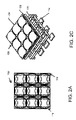
- FIG. 2A is a top view of a portion of a silicon die in accordance with one embodiment of the present teachings.
- FIGS. 2B , 2 C and 2 D are a front, perspective and side view of the portion in FIG. 2A , respectively
- FIGS. 3A and 3B illustrate ray acceptance angles for a sensor with a non-shifted microlens array.
- FIG. 4 is an image of a white light source captured by an image sensor having a sensor die, where the brightness of the image is non-uniform across the sensor die.
- FIGS. 5A and 5B illustrate ray acceptance angles for a sensor with a shifted microlens array in accordance with one embodiment of the present teachings.
- FIG. 6 is a top view of a sensor die with a microlens array, elements of which are shifted to achieve ray angle match over the entire sensor die in accordance with one embodiment of the present teachings.
- FIG. 7A is a top view of a typical pixel, where a metal layer is blocking a corner of the photodiode of each pixel.
- FIGS. 7B-D are cross sectional views of three pixels located at edges of a sensor die, illustrating the interference of light rays with a metal layer shown in FIG. 7A .
- FIG. 7E is an image of a white light source captured by a typical image sensor having pixels with metal layer as shown in FIG. 7A .
- FIG. 8A is a top view of a pixel, illustrating an area where metal layers can be located without blocking optical rays collected by a photodiode of the pixel in accordance with one embodiment of the present teachings.
- FIG. 8B is a cross sectional view of a pixel shown in FIG. 8A .
- FIG. 9 shows a flow chart, illustrating exemplary steps for configuring metal layout of a pixel in a sensor die to enhance intensity uniformity of an image captured by the sensor die in accordance with one embodiment of the present teachings.
- FIG. 10 shows an arrangement of identical pixels on a sensor die to minimize chief ray angles in accordance with one embodiment of the present teachings.
- FIG. 11A is a top view of a typical pixel, where a metal layer is blocking a central portion of the photodiode of each pixel.
- FIG. 11B is an image of a white light source captured by an image sensor having pixels with metal layer as shown in FIG. 11A .
- FIGS. 11C-D are top views of pixels illustrating the effect of the image size captured by each microlens on the non-uniformity shown in FIG. 11B .
- microlens includes a plurality of such microlens, i.e., microlens array, and equivalents thereof known to those skilled in the art, and so forth.
- CMOS sensor customization is shifting a microlens array of the sensor to match incident rays at large angles.
- the non-symmetric nature of the CMOS sensor layout may create non-symmetric brightness distribution over the image output, where the non-symmetric nature may be more pronounced at the corners and edges of the image output.
- non-symmetric brightness may be accompanied by improper color balance, i.e., the color of the image of a white light source is not white over the entire image output.
- the present inventor provides a simple, yet effective way to resolve the appearance of non-symmetric brightness in the image by introducing off-center alignment between a microlens array and a sensor pixel array of the CMOS sensor.
- FIG. 1 is a schematic diagram of an image module assembly 100 (or, equivalently a lens/sensor assembly) in accordance with one embodiment of the present teachings.
- the lens/sensor assembly 100 may be included in digital image devices, such as digital image camera and cellular phone with imaging capabilities.
- the lens/sensor assembly 100 includes: a sensor die 108 as an image sensor; and a lens assembly 102 having several pieces of lenses and iris (not shown in FIG. 1 for simplicity) assembled in a lens barrel, the lens assembly forming an image on the surface of the sensor die 108 .
- the width and length of the sensor die 108 is about, but not limited to, 5 mm.
- Optical rays 104 a - c exemplary optical rays from the lens assembly 102 , are directed to sensor pixels (the sensor pixels will be explained later) at the center, near the left edge and near the right edge of the sensor die 108 , respectively, and angled with respect to the surface normal of the sensor die 108 by chief ray angles 106 a - c , respectively.
- the chief ray angles 106 b and 106 c may be as large as 30 degrees, while the chief ray angle 106 a is about zero degree.
- the sensor die 108 is a piece of silicon that includes an integrated circuit (IC) to function as an image sensor.
- the IC comprises a processing area and a sensing area that may have from several hundred thousands to millions of identical sensor pixels.
- the sensor die 108 refers to its sensing area only.
- FIG. 2A is a top view of a portion 109 of the silicon die 108 in accordance with one embodiment of the present teachings, where only 9 sensor pixels 110 are shown for simplicity.
- FIGS. 2B and 2D are the front and side views of the portion 109 in FIG. 2A , respectively, showing multiple layers 112 - 138 of the silicon die 108 .
- FIG. 2C is a perspective view of the portion 109 in FIG. 2A , focusing on several key features of the layers.
- each pixel 110 includes: a silicon substrate layer 112 ; a photodiode 114 forming a portion of and being underneath the surface of the silicon substrate layer 112 ; a plurality of passive components 115 (such as transistors, resistors and capacitors) underneath the surface of the silicon substrate layer 112 ; four transparent insulating layers 116 , 120 , 124 and 128 ; four metal layers 118 , 122 , 126 and 130 , the four metal layers being insulated by the four transparent insulating layers 116 , 120 , 124 and 128 , and connected to the photodiode 114 and/or the plurality of passive elements 115 ; a first planar layer 132 , the first planar layer being a transparent insulating layer and having a flat top surface; a color filter 134 for passing a specific wavelength or wavelength band of light to the photodiode 114 ; and a microlens 138 for focusing light rays
- the photodiode 114 and the plurality of passive elements 115 may be formed by a semiconductor etching process, i.e., etching the surface of the silicon substrate layer 112 and chemically depositing intended types of material on the etched area to form the photodiode 114 and the plurality of passive elements 115 .
- the color filter 134 filters light rays (such as 104 in FIG. 1 ) directed to its corresponding photodiode 114 and transmits light rays of only one wavelength or wavelength band.
- a RGB color system may be used, and consequently, a color filter array (CFA) 135 (shown in FIG. 2C ) comprises three types of filters 134 .
- CFA color filter array
- signals from three pixels are needed to form one complete color.
- the number of types of filters in the CFA 135 can vary depending on the color system applied to the silicon die 108 .
- the metal layers 118 , 122 , 126 and 130 function as connecting means for the photodiodes 114 and passive components 115 to the processing area of the silicon die 108 , where the signals from the photodiodes and passive components are transmitted using a column transfer method.
- exemplary connections 119 and 121 are shown, where the connections 119 and 121 link the metal layer 118 to the photodiode 114 and one the of passive components 115 , respectively.
- connections between the four metal layers ( 118 , 122 , 126 and 130 ) and the photodiode 114 and the passive components 115 can vary depending on the overall layout of the silicon die 108 .
- the number of metal layers depends on the complexity of the layout of metal layers and, as a consequence, a different layout of the silicon die may have a different number of metal layers.
- each of the optical rays 104 a - c is angled with respect to the surface normal of the sensor die 108 .
- FIGS. 3A and 3B illustrate ray acceptance angles 306 for a sensor die 308 with a non-shifted microlens array 304 , where the optical axis of a microlens in each pixel 310 coincides with the optical axis of a photodiode 302 in the pixel.
- the optical axis of a photodiode refers to an axis normal to the surface of the photodiode and passes through the geometric center of the photodiode.
- FIG. 3A-3B for simplicity, only photodiodes 302 and a microlens array 304 are shown.
- FIG. 3A most of the light rays 104 a are collected by a photodiode 302 a that is located at the center of the sensor die 308 .
- the light ray acceptance angle 306 a is the same as that of incoming light rays 104 a .
- FIG. 3B some portion of the optical rays 104 b are not collected by a photodiode 302 b that is located near the right edge of the silicon die 308 , i.e., the photodiode 302 b has a limited ray acceptance angle 306 b .
- FIG. 4 shows an image 400 of a white light source captured by an image sensor having the sensor die 308 , where the brightness of image 400 is non-uniform across the sensor die 308 , where the brightness of image 400 is non-uniform across the sensor die 308 .
- the image 400 may not be color balanced, i.e., the color of the image is not white over the entire sensor die.
- FIGS. 5A and 5B illustrate ray acceptance angles 506 for a sensor die 508 , where the optical axis of a microlens 504 in each pixel 510 has been shifted with respect to the optical axis of a photodiode 502 of the pixel in accordance with one embodiment of the present teachings.
- the optical axis of a microlens 504 a in a pixel coincides with the optical axis of a photodiode 502 a of the same pixel, where the pixel is located at the center of the sensor die 508 .
- FIG. 5A the optical axis of a microlens 504 a in a pixel coincides with the optical axis of a photodiode 502 a of the same pixel, where the pixel is located at the center of the sensor die 508 .
- FIG. 5A illustrates ray acceptance angles 506 for a sensor die 508 , where the optical axis of a microlen
- the optical axis of a microlens 504 b in a pixel located near the right edge of the sensor die 508 has been shifted by a distance 512 with respect to the optical axis of a photodiode 502 b in an effort to improve the ray acceptance angle 506 b .
- the light ray acceptance angles 506 a and 506 b are equal to those of the incoming light rays 104 a and 104 b , respectively.
- FIG. 6 is a top view of a sensor die 600 with a microlens array 602 , the elements of which are shifted to achieve ray angle match over the entire sensor die 600 in accordance with one embodiment of the present teachings.
- FIG. 6 for simplicity, only the array of microlens 602 and photodiodes 604 are shown.
- each microlens 602 has been shifted toward the center 612 of the sensor die 600 so that each of light spots 606 is located within the corresponding photodiode 604 , which improves the ray acceptance angle, and subsequently, the brightness distribution of image on the silicon die 600 .
- each microlens is more pronounced near sensor edges 610 and corners 608 than the center 612 .
- the shifting of each microlens is implemented by scaling a photo mask of the microlens array 602 .
- Detailed description of shifting each microlens is disclosed in U.S. patent application Ser. No. 11/004,465, entitled “Microlens alignment procedures in CMOS image sensor design,” which is hereby incorporated herein by reference in its entirety.
- FIG. 7A shows a top view of a typical pixel 702 , illustrating a detailed layout of metal layers 704 , 706 and photodiode 708 .
- Metal layers 704 and 706 may be formed of an opaque material, such as aluminum, and define the shape of openings 710 through which the light rays directed to photodiode 708 are collected. As shown in FIG. 7A , the shape of the opening 710 may not be axially symmetric with respect to the axis that is surface normal and passes through the geometric center of photodiode 708 .
- FIGS. 7B-D show cross sectional views of three pixels 714 a - c located at 610 a , 612 , and 610 c ( FIG. 6 ), respectively, along line A-A of FIG. 7A , illustrating the interference of metal layer 704 with light rays 722 a - c .
- microlenses 720 a - c have been shifted with respect to photodiode 708 to optimize the ray acceptance angle.
- the blockage of light by metal layer 704 is the most significant at pixel 714 a and becomes less pronounced as it moves toward the pixel 714 c , which results non-uniform intensity distribution of image 740 shown in FIG. 7E .
- FIG. 8A shows a top view of a pixel 802 , illustrating photodiode 804 and an exemplary area 806 where metal layers can be located without blocking optical rays collected by the photodiode 804 in accordance with one embodiment of the present teachings.
- Inner boundary 808 of area 806 can be determined by conventional ray trace method as shown in FIG. 8B .
- edge pixel 802 is a cross sectional view of an edge pixel 802 along the line B-B, where the term “edge pixel” refers to one of pixels located along four edges of a sensor die. For simplicity, microlens is not shown in FIG. 8B .
- Distance 810 represents the vertical interval between photodiode 804 and plane 814 defined by a metal layer 812 .
- a portion 818 is an area where plane 814 crosses optical rays 816 collected by photodiode 804 , wherein surface normal 822 makes an angle 820 with optical ray 816 .
- Boundary 808 is defined by the edge of the area that is formed by adding portions 818 for all edge pixels.
- FIG. 9 shows a flow chart 900 , illustrating exemplary steps for determining area where the metal layout of a pixel in a sensor die can be configured to enhance intensity uniformity of an image captured by the sensor die.
- an edge pixel of the sensor die is selected.
- a microlens of the edge pixel is shifted toward center of the sensor die to maximize ray acceptance angle for the edge pixel.
- a plane parallel to a photodiode of the edge pixel is considered at step 906 .
- a portion of the plane is laid out such that all of the optical rays collected by the microlens pass through the portion.
- the metal layer is configured at step 910 to be outside of the determined portion such that interference of the metal layer with optical rays is eliminated and uniformity of image intensity is enhanced.
- FIG. 10 illustrates an arrangement of identical pixels 1002 for a sensor die 1000 in accordance with one embodiment of the present teachings, where the photodiode of each pixel is of a polygonal shape 1004 .
- typical sensor die 1000 has width 1006 that is larger than length 1008 , and pixels 1002 are arranged such that the longest side 1010 of the polygon 1004 is in parallel with width 1006 . In such an arrangement, the ratio of the microlens shift for an edge pixel to its photodiode dimension is minimized, which yields the minimum of angle 820 .
- FIG. 11A is a top view of a typical pixel 1102 , where a metal layer 1106 extrudes toward the center of the photodiode 1108 .
- a metal layer 1106 extrudes toward the center of the photodiode 1108 .
- the intensity of image 1109 may have non-uniformity as shown in FIG. 11B .
- FIG. 11C shows a top view of a pixel 1110 illustrating a portion of the metal layer 1106 overlapped with three circles 1112 a - c , where each circle corresponds to an image on the photodiode 1108 focused by a microlens in an edge pixel.
- FIG. 11D shows a similar top view of a pixel 1114 illustrating three circles 1116 a - c that have a larger diameter than the three circles 1112 a - c .
- the blocked area by the metal layer 1106 may be substantially the same for both circles 1112 b and 1116 b .
- the ratio of the blocked area to the circle area may be smaller in the case of the larger circle 1116 b than the smaller circle 1112 b , which yields less difference in intensity between the central and edge pixels.
- the size of the image 1116 a - c can be controlled by the focal length of a microlens or the distance from the microlens to the photodiode. It is desirable to have a minimum distance from the microlens to the photodiode in the design to have the best efficiency.
- the size of the image can be controlled by microlens focal length with specific center thickness of the microlens.
Landscapes
- Solid State Image Pick-Up Elements (AREA)
- Transforming Light Signals Into Electric Signals (AREA)
Abstract
Description
Claims (19)
Priority Applications (1)
| Application Number | Priority Date | Filing Date | Title |
|---|---|---|---|
| US11/004,376 US7763918B1 (en) | 2004-12-02 | 2004-12-02 | Image pixel design to enhance the uniformity of intensity distribution on digital image sensors |
Applications Claiming Priority (1)
| Application Number | Priority Date | Filing Date | Title |
|---|---|---|---|
| US11/004,376 US7763918B1 (en) | 2004-12-02 | 2004-12-02 | Image pixel design to enhance the uniformity of intensity distribution on digital image sensors |
Publications (1)
| Publication Number | Publication Date |
|---|---|
| US7763918B1 true US7763918B1 (en) | 2010-07-27 |
Family
ID=42341878
Family Applications (1)
| Application Number | Title | Priority Date | Filing Date |
|---|---|---|---|
| US11/004,376 Active 2026-06-02 US7763918B1 (en) | 2004-12-02 | 2004-12-02 | Image pixel design to enhance the uniformity of intensity distribution on digital image sensors |
Country Status (1)
| Country | Link |
|---|---|
| US (1) | US7763918B1 (en) |
Cited By (4)
| Publication number | Priority date | Publication date | Assignee | Title |
|---|---|---|---|---|
| US20090033788A1 (en) * | 2007-08-02 | 2009-02-05 | Micron Technology, Inc. | Integrated optical characteristic measurements in a cmos image sensor |
| WO2020251904A1 (en) * | 2019-06-10 | 2020-12-17 | Gigajot Technology, Inc. | Cmos image sensors with per-pixel micro-lens arrays |
| US11456327B2 (en) * | 2019-03-06 | 2022-09-27 | Samsung Electronics Co., Ltd. | Image sensor and imaging device |
| CN120219371A (en) * | 2025-05-21 | 2025-06-27 | 宝鸡龙恒达铝业有限公司 | Aluminum profile extrusion molding monitoring method and system based on machine vision |
Citations (39)
| Publication number | Priority date | Publication date | Assignee | Title |
|---|---|---|---|---|
| US4739394A (en) | 1985-07-17 | 1988-04-19 | Fuji Photo Film Co., Ltd. | White balanced electronic still camera |
| US5142357A (en) | 1990-10-11 | 1992-08-25 | Stereographics Corp. | Stereoscopic video camera with image sensors having variable effective position |
| US5323052A (en) * | 1991-11-15 | 1994-06-21 | Sharp Kabushiki Kaisha | Image pickup device with wide angular response |
| US5324930A (en) * | 1993-04-08 | 1994-06-28 | Eastman Kodak Company | Lens array for photodiode device with an aperture having a lens region and a non-lens region |
| US5422285A (en) * | 1992-05-27 | 1995-06-06 | Sharp Kabushiki Kaisha | Method of producing solid-state imaging device |
| US5659357A (en) | 1995-04-13 | 1997-08-19 | Eastman Kodak Company | Auto white adjusting device |
| US5798847A (en) | 1995-05-24 | 1998-08-25 | Oce-Nederland B.V. | Method of and apparatus for correcting the output signals of an array of photodetector elements |
| US5838023A (en) | 1995-09-07 | 1998-11-17 | Hewlett-Packard Company | Ancillary pads for on-circuit array probing composed of I/O and test pads |
| US6008511A (en) * | 1996-10-21 | 1999-12-28 | Kabushiki Kaisha Toshiba | Solid-state image sensor decreased in shading amount |
| US6246043B1 (en) | 1998-09-22 | 2001-06-12 | Foveon, Inc. | Method and apparatus for biasing a CMOS active pixel sensor above the nominal voltage maximums for an IC process |
| US6274917B1 (en) * | 1999-10-12 | 2001-08-14 | Taiwan Semiconductor Manufacturing Company | High efficiency color filter process for semiconductor array imaging devices |
| US20010036305A1 (en) | 1999-12-30 | 2001-11-01 | Sung-Chun Jun | Detecting and compensating defective pixels in image sensor on real time basis |
| US20010056337A1 (en) | 2000-04-10 | 2001-12-27 | Shunji Kurita | Method of designing position of micro-lens for optical panel device, method of producing optical panel device, and optical panel device |
| US6411331B1 (en) | 1997-02-28 | 2002-06-25 | Hewlett-Packard Company | Automatic white balance detection and correction of an image captured in a digital camera |
| US6437307B1 (en) | 1997-09-12 | 2002-08-20 | Fraunhofer-Gesellschaft Zur Forderung Zur Angewandten Forshung E.V. | Image detection member and assembly of image detection members |
| US20030006363A1 (en) * | 2001-04-27 | 2003-01-09 | Campbell Scott Patrick | Optimization of alignment between elements in an image sensor |
| US20030011686A1 (en) | 2001-06-01 | 2003-01-16 | Olympus Optical Co., Ltd. | Digital camera and white balance adjusting method |
| US20030071271A1 (en) * | 1999-12-02 | 2003-04-17 | Satoshi Suzuki | Solid-state image sensor, production method of the same, and digital camera |
| US20030173599A1 (en) | 2002-01-31 | 2003-09-18 | Junichi Nakai | Semiconductor device and fabrication method therefor |
| WO2004027875A1 (en) | 2002-09-20 | 2004-04-01 | Sony Corporation | Solid state imaging device and production method therefor |
| US6747808B2 (en) | 2002-10-04 | 2004-06-08 | Hewlett-Packard Development Company, L.P. | Electronic imaging device focusing |
| US20040135899A1 (en) | 2003-01-10 | 2004-07-15 | Kazunori Suemoto | Image pick-up apparatus and white balance control method |
| US20040140564A1 (en) | 2003-01-16 | 2004-07-22 | Soo-Geun Lee | Structure of a CMOS image sensor and method for fabricating the same |
| US6781632B1 (en) * | 1999-04-20 | 2004-08-24 | Olympus Corporation | Image pick-up apparatus capable of focus detection |
| US20040165097A1 (en) * | 2002-10-11 | 2004-08-26 | Drowley Clifford I. | Microlens for use with a solid-state image sensor and a non-telecentric taking lens |
| US6838715B1 (en) * | 2002-04-30 | 2005-01-04 | Ess Technology, Inc. | CMOS image sensor arrangement with reduced pixel light shadowing |
| US20050010621A1 (en) | 2003-07-07 | 2005-01-13 | Victor Pinto | Dynamic identification and correction of defective pixels |
| US20050061951A1 (en) * | 2001-04-27 | 2005-03-24 | Campbell Scott P. | Optimization of alignment among elements in an image sensor |
| US6884985B2 (en) | 2000-12-08 | 2005-04-26 | Stmicroelectronics Ltd. | Solid state image sensors and microlens arrays |
| US6903391B2 (en) * | 2003-09-10 | 2005-06-07 | Fuji Photo Film Co., Ltd. | Solid state image pickup device |
| US20050122408A1 (en) | 2003-12-03 | 2005-06-09 | Park Hyung M. | Digital automatic white balance device |
| US20050174473A1 (en) | 1999-11-18 | 2005-08-11 | Color Kinetics, Inc. | Photography methods and systems |
| US6995800B2 (en) * | 2000-01-27 | 2006-02-07 | Canon Kabushiki Kaisha | Image pickup apparatus utilizing a plurality of converging lenses |
| US7006135B2 (en) | 2001-06-15 | 2006-02-28 | Olympus Corporation | Camera capable of white balance correction |
| US7019279B2 (en) * | 2002-11-07 | 2006-03-28 | Fuji Photo Film Co., Ltd. | Solid-state image sensor with the optical center of microlenses shifted from the center of photo-sensors for increasing the convergence ratio |
| US7049168B2 (en) * | 2004-05-28 | 2006-05-23 | Stmicroelectronics Ltd. | Image sensor comprising a pixel array having an optical element positioned relative to each pixel |
| US20060113622A1 (en) | 2004-11-30 | 2006-06-01 | International Business Machines Corporation | A damascene copper wiring image sensor |
| US7161129B2 (en) * | 2004-09-10 | 2007-01-09 | Transchip, Inc. | Image capture device, including methods for arranging the optical components thereof |
| US7236190B2 (en) | 2002-10-31 | 2007-06-26 | Freescale Semiconductor, Inc. | Digital image processing using white balance and gamma correction |
-
2004
- 2004-12-02 US US11/004,376 patent/US7763918B1/en active Active
Patent Citations (40)
| Publication number | Priority date | Publication date | Assignee | Title |
|---|---|---|---|---|
| US4739394A (en) | 1985-07-17 | 1988-04-19 | Fuji Photo Film Co., Ltd. | White balanced electronic still camera |
| US5142357A (en) | 1990-10-11 | 1992-08-25 | Stereographics Corp. | Stereoscopic video camera with image sensors having variable effective position |
| US5323052A (en) * | 1991-11-15 | 1994-06-21 | Sharp Kabushiki Kaisha | Image pickup device with wide angular response |
| US5422285A (en) * | 1992-05-27 | 1995-06-06 | Sharp Kabushiki Kaisha | Method of producing solid-state imaging device |
| US5324930A (en) * | 1993-04-08 | 1994-06-28 | Eastman Kodak Company | Lens array for photodiode device with an aperture having a lens region and a non-lens region |
| US5659357A (en) | 1995-04-13 | 1997-08-19 | Eastman Kodak Company | Auto white adjusting device |
| US5798847A (en) | 1995-05-24 | 1998-08-25 | Oce-Nederland B.V. | Method of and apparatus for correcting the output signals of an array of photodetector elements |
| US5838023A (en) | 1995-09-07 | 1998-11-17 | Hewlett-Packard Company | Ancillary pads for on-circuit array probing composed of I/O and test pads |
| US6008511A (en) * | 1996-10-21 | 1999-12-28 | Kabushiki Kaisha Toshiba | Solid-state image sensor decreased in shading amount |
| US6411331B1 (en) | 1997-02-28 | 2002-06-25 | Hewlett-Packard Company | Automatic white balance detection and correction of an image captured in a digital camera |
| US6437307B1 (en) | 1997-09-12 | 2002-08-20 | Fraunhofer-Gesellschaft Zur Forderung Zur Angewandten Forshung E.V. | Image detection member and assembly of image detection members |
| US6246043B1 (en) | 1998-09-22 | 2001-06-12 | Foveon, Inc. | Method and apparatus for biasing a CMOS active pixel sensor above the nominal voltage maximums for an IC process |
| US6781632B1 (en) * | 1999-04-20 | 2004-08-24 | Olympus Corporation | Image pick-up apparatus capable of focus detection |
| US6274917B1 (en) * | 1999-10-12 | 2001-08-14 | Taiwan Semiconductor Manufacturing Company | High efficiency color filter process for semiconductor array imaging devices |
| US20050174473A1 (en) | 1999-11-18 | 2005-08-11 | Color Kinetics, Inc. | Photography methods and systems |
| US20030071271A1 (en) * | 1999-12-02 | 2003-04-17 | Satoshi Suzuki | Solid-state image sensor, production method of the same, and digital camera |
| US20010036305A1 (en) | 1999-12-30 | 2001-11-01 | Sung-Chun Jun | Detecting and compensating defective pixels in image sensor on real time basis |
| US6995800B2 (en) * | 2000-01-27 | 2006-02-07 | Canon Kabushiki Kaisha | Image pickup apparatus utilizing a plurality of converging lenses |
| US20010056337A1 (en) | 2000-04-10 | 2001-12-27 | Shunji Kurita | Method of designing position of micro-lens for optical panel device, method of producing optical panel device, and optical panel device |
| US6884985B2 (en) | 2000-12-08 | 2005-04-26 | Stmicroelectronics Ltd. | Solid state image sensors and microlens arrays |
| US20030006363A1 (en) * | 2001-04-27 | 2003-01-09 | Campbell Scott Patrick | Optimization of alignment between elements in an image sensor |
| US20050061951A1 (en) * | 2001-04-27 | 2005-03-24 | Campbell Scott P. | Optimization of alignment among elements in an image sensor |
| US20030011686A1 (en) | 2001-06-01 | 2003-01-16 | Olympus Optical Co., Ltd. | Digital camera and white balance adjusting method |
| US7006135B2 (en) | 2001-06-15 | 2006-02-28 | Olympus Corporation | Camera capable of white balance correction |
| US20030173599A1 (en) | 2002-01-31 | 2003-09-18 | Junichi Nakai | Semiconductor device and fabrication method therefor |
| US6838715B1 (en) * | 2002-04-30 | 2005-01-04 | Ess Technology, Inc. | CMOS image sensor arrangement with reduced pixel light shadowing |
| WO2004027875A1 (en) | 2002-09-20 | 2004-04-01 | Sony Corporation | Solid state imaging device and production method therefor |
| US20060006438A1 (en) * | 2002-09-20 | 2006-01-12 | Yasushi Maruyama | Solid state imaging device and production method therefor |
| US6747808B2 (en) | 2002-10-04 | 2004-06-08 | Hewlett-Packard Development Company, L.P. | Electronic imaging device focusing |
| US20040165097A1 (en) * | 2002-10-11 | 2004-08-26 | Drowley Clifford I. | Microlens for use with a solid-state image sensor and a non-telecentric taking lens |
| US7236190B2 (en) | 2002-10-31 | 2007-06-26 | Freescale Semiconductor, Inc. | Digital image processing using white balance and gamma correction |
| US7019279B2 (en) * | 2002-11-07 | 2006-03-28 | Fuji Photo Film Co., Ltd. | Solid-state image sensor with the optical center of microlenses shifted from the center of photo-sensors for increasing the convergence ratio |
| US20040135899A1 (en) | 2003-01-10 | 2004-07-15 | Kazunori Suemoto | Image pick-up apparatus and white balance control method |
| US20040140564A1 (en) | 2003-01-16 | 2004-07-22 | Soo-Geun Lee | Structure of a CMOS image sensor and method for fabricating the same |
| US20050010621A1 (en) | 2003-07-07 | 2005-01-13 | Victor Pinto | Dynamic identification and correction of defective pixels |
| US6903391B2 (en) * | 2003-09-10 | 2005-06-07 | Fuji Photo Film Co., Ltd. | Solid state image pickup device |
| US20050122408A1 (en) | 2003-12-03 | 2005-06-09 | Park Hyung M. | Digital automatic white balance device |
| US7049168B2 (en) * | 2004-05-28 | 2006-05-23 | Stmicroelectronics Ltd. | Image sensor comprising a pixel array having an optical element positioned relative to each pixel |
| US7161129B2 (en) * | 2004-09-10 | 2007-01-09 | Transchip, Inc. | Image capture device, including methods for arranging the optical components thereof |
| US20060113622A1 (en) | 2004-11-30 | 2006-06-01 | International Business Machines Corporation | A damascene copper wiring image sensor |
Non-Patent Citations (18)
| Title |
|---|
| Nikon, AF Micro-Nikkor 60mm f/2.8D 1993, Release: http://nikonimaging.com/global/products/lens/af/micro/af-micro60mmf-28d/index.htm. |
| Nikon, AF Micro-Nikkor 60mm f/2.8D 1993, Release: http://nikonimaging.com/global/products/lens/af/micro/af—micro60mmf—28d/index.htm. |
| Notice of Allowance issued in U.S. Appl. No. 11/003,824 mailed Jul. 15, 2008. |
| Notice of Allowance issued in U.S. Appl. No. 11/313,976, mailed Mar. 24, 2009. |
| Office Action issued in U.S. Appl. No. 10/976,693, mailed Jun. 11, 2008. |
| Office Action issued in U.S. Appl. No. 10/976,693, mailed Oct. 18, 2007. |
| Office Action issued in U.S. Appl. No. 11/003,824, mailed Dec. 12, 2007. |
| Office Action issued in U.S. Appl. No. 11/004,465, mailed Aug. 28, 2006. |
| Office Action issued in U.S. Appl. No. 11/004,465, mailed Jan. 11, 2008. |
| Office Action issued in U.S. Appl. No. 11/004,465, mailed Jan. 25, 2007. |
| Office Action issued in U.S. Appl. No. 11/004,465, mailed Jun. 2, 2008. |
| Office Action issued in U.S. Appl. No. 11/004,465, mailed Mar. 28, 2006. |
| Office Action issued in U.S. Appl. No. 11/004,465, mailed Oct. 2, 2008. |
| Office Action issued in U.S. Appl. No. 11/314,452, mailed Aug. 9, 2007. |
| Office Action issued in U.S. Appl. No. 11/314,452, mailed Dec. 22, 2008. |
| Office Action issued in U.S. Appl. No. 11/314,452, mailed Jan. 5, 2007. |
| Office Action issued in U.S. Appl. No. 11/314,452, mailed Jun. 30, 2006. |
| Office Action issued in U.S. Appl. No. 11/314,452, mailed Mar. 17, 2008. |
Cited By (7)
| Publication number | Priority date | Publication date | Assignee | Title |
|---|---|---|---|---|
| US20090033788A1 (en) * | 2007-08-02 | 2009-02-05 | Micron Technology, Inc. | Integrated optical characteristic measurements in a cmos image sensor |
| US8085391B2 (en) * | 2007-08-02 | 2011-12-27 | Aptina Imaging Corporation | Integrated optical characteristic measurements in a CMOS image sensor |
| US11456327B2 (en) * | 2019-03-06 | 2022-09-27 | Samsung Electronics Co., Ltd. | Image sensor and imaging device |
| WO2020251904A1 (en) * | 2019-06-10 | 2020-12-17 | Gigajot Technology, Inc. | Cmos image sensors with per-pixel micro-lens arrays |
| US11276721B2 (en) * | 2019-06-10 | 2022-03-15 | Gigajot Technology, Inc. | CMOS image sensors with per-pixel micro-lens arrays |
| US12426393B2 (en) | 2019-06-10 | 2025-09-23 | Gigajot Technology, Inc. | CMOS image sensors with per-pixel micro-lens arrays |
| CN120219371A (en) * | 2025-05-21 | 2025-06-27 | 宝鸡龙恒达铝业有限公司 | Aluminum profile extrusion molding monitoring method and system based on machine vision |
Similar Documents
| Publication | Publication Date | Title |
|---|---|---|
| US11323608B2 (en) | Image sensors with phase detection auto-focus pixels | |
| JP5646445B2 (en) | Thin camera with sub-pixel resolution | |
| KR102004647B1 (en) | Backside illumination image sensor, manufacturing method thereof and image-capturing device | |
| CN112889064B (en) | Biometric Imaging Unit Below Display | |
| US9261769B2 (en) | Imaging apparatus and imaging system | |
| US11765476B2 (en) | Imaging element and method for manufacturing imaging element | |
| CN100356573C (en) | Solid state imaging device | |
| CN106068563A (en) | Solid-state imaging device, manufacturing method of solid-state imaging device, and electronic device | |
| CN107615484B (en) | Solid-state imaging device, imaging device, and manufacturing method of solid-state imaging device | |
| EP2669949B1 (en) | Lens array for partitioned image sensor | |
| WO2015122300A1 (en) | Imaging element, manufacturing device, and electronic device | |
| US20080142685A1 (en) | Integrated image sensor having a color-filtering microlens, and related system and method | |
| CN110050343A (en) | Photographing element and focus-regulating device | |
| US8068284B2 (en) | Microlens alignment procedures in CMOS image sensor design | |
| US7297916B1 (en) | Optically improved CMOS imaging sensor structure to lower imaging lens requirements | |
| JPH05167054A (en) | Manufacture of solid-state image sensing device | |
| US8149322B2 (en) | Image sensor with an improved sensitivity | |
| JPH09148549A (en) | Color solid-state image sensor with on-chip lens | |
| KR20100067982A (en) | Image sensor and method for fabricating the same | |
| US7763918B1 (en) | Image pixel design to enhance the uniformity of intensity distribution on digital image sensors | |
| TW201444069A (en) | Solid-state imaging device, manufacturing method thereof, and electronic device | |
| CN111837131A (en) | Fingerprint identification devices and electronic equipment | |
| CN100429779C (en) | Image sensor and manufacturing method thereof | |
| US7450161B1 (en) | System and method to enhance the uniformity of intensity distribution on digital imaging sensors | |
| CN110036481A (en) | Photographing element and focus-regulating device |
Legal Events
| Date | Code | Title | Description |
|---|---|---|---|
| AS | Assignment |
Owner name: IC MEDIA CORPORATION, CALIFORNIA Free format text: ASSIGNMENT OF ASSIGNORS INTEREST;ASSIGNORS:FENG, CHEN;LI, JIM;REEL/FRAME:016054/0037 Effective date: 20041202 |
|
| AS | Assignment |
Owner name: BANK OF NEW YORK, THE, NEW YORK Free format text: SECURITY INTEREST;ASSIGNOR:IC MEDIA CORPORATION;REEL/FRAME:016500/0697 Effective date: 20041223 Owner name: UBS AG, STAMFORD BRANCH, CONNECTICUT Free format text: SECURITY AGREEMENT;ASSIGNOR:IC MEDIA CORPORATION;REEL/FRAME:016522/0420 Effective date: 20050531 |
|
| AS | Assignment |
Owner name: MAGNACHIP SEMICONDUCTOR, INC., CALIFORNIA Free format text: CHANGE OF NAME;ASSIGNOR:IC MEDIA CORPORATION;REEL/FRAME:017344/0427 Effective date: 20051117 |
|
| AS | Assignment |
Owner name: MAGNACHIP SEMICONDUCTOR, INC., CALIFORNIA Free format text: MERGER;ASSIGNOR:IC MEDIA CORPORATION;REEL/FRAME:018095/0114 Effective date: 20051117 |
|
| AS | Assignment |
Owner name: MAGNACHIP SEMICONDUCTOR LTD., KOREA, REPUBLIC OF Free format text: INTERSUBSIDIARY ASSET TRANSFER AGREEMENT;ASSIGNOR:MAGNACHIP SEMICONDUCTOR INC.;REEL/FRAME:018943/0886 Effective date: 20070101 |
|
| AS | Assignment |
Owner name: MAGNACHIP SEMICONDUCTOR LTD., KOREA, REPUBLIC OF Free format text: NUNC PRO TUNC ASSIGNMENT;ASSIGNOR:MAGNACHIP SEMICONDUCTOR INC.;REEL/FRAME:022732/0296 Effective date: 20090514 Owner name: IC MEDIA CORPORATION, CALIFORNIA Free format text: ASSIGNMENT OF ASSIGNORS INTEREST;ASSIGNORS:FENG, CHEN;LI, JIM;REEL/FRAME:022740/0338 Effective date: 20090522 |
|
| AS | Assignment |
Owner name: CROSSTEK CAPITAL, LLC, DELAWARE Free format text: ASSIGNMENT OF ASSIGNORS INTEREST;ASSIGNOR:MAGNACHIP SEMICONDUCTOR, LTD.;REEL/FRAME:022764/0270 Effective date: 20090514 |
|
| STCF | Information on status: patent grant |
Free format text: PATENTED CASE |
|
| AS | Assignment |
Owner name: INTELLECTUAL VENTURES II LLC, DELAWARE Free format text: MERGER;ASSIGNOR:CROSSTEK CAPITAL, LLC;REEL/FRAME:026637/0632 Effective date: 20110718 |
|
| FPAY | Fee payment |
Year of fee payment: 4 |
|
| MAFP | Maintenance fee payment |
Free format text: PAYMENT OF MAINTENANCE FEE, 8TH YEAR, LARGE ENTITY (ORIGINAL EVENT CODE: M1552) Year of fee payment: 8 |
|
| MAFP | Maintenance fee payment |
Free format text: PAYMENT OF MAINTENANCE FEE, 12TH YEAR, LARGE ENTITY (ORIGINAL EVENT CODE: M1553); ENTITY STATUS OF PATENT OWNER: LARGE ENTITY Year of fee payment: 12 |