US7763509B2 - Method of manufacturing semiconductor device including forming two stress films and irradiation of one stress film - Google Patents
Method of manufacturing semiconductor device including forming two stress films and irradiation of one stress film Download PDFInfo
- Publication number
- US7763509B2 US7763509B2 US11/639,344 US63934406A US7763509B2 US 7763509 B2 US7763509 B2 US 7763509B2 US 63934406 A US63934406 A US 63934406A US 7763509 B2 US7763509 B2 US 7763509B2
- Authority
- US
- United States
- Prior art keywords
- film
- stress film
- mosfet
- irradiation
- tensile stress
- Prior art date
- Legal status (The legal status is an assumption and is not a legal conclusion. Google has not performed a legal analysis and makes no representation as to the accuracy of the status listed.)
- Expired - Fee Related, expires
Links
Images


Classifications
-
- H—ELECTRICITY
- H10—SEMICONDUCTOR DEVICES; ELECTRIC SOLID-STATE DEVICES NOT OTHERWISE PROVIDED FOR
- H10D—INORGANIC ELECTRIC SEMICONDUCTOR DEVICES
- H10D30/00—Field-effect transistors [FET]
- H10D30/60—Insulated-gate field-effect transistors [IGFET]
- H10D30/791—Arrangements for exerting mechanical stress on the crystal lattice of the channel regions
- H10D30/792—Arrangements for exerting mechanical stress on the crystal lattice of the channel regions comprising applied insulating layers, e.g. stress liners
-
- H—ELECTRICITY
- H10—SEMICONDUCTOR DEVICES; ELECTRIC SOLID-STATE DEVICES NOT OTHERWISE PROVIDED FOR
- H10D—INORGANIC ELECTRIC SEMICONDUCTOR DEVICES
- H10D84/00—Integrated devices formed in or on semiconductor substrates that comprise only semiconducting layers, e.g. on Si wafers or on GaAs-on-Si wafers
- H10D84/01—Manufacture or treatment
- H10D84/0123—Integrating together multiple components covered by H10D12/00 or H10D30/00, e.g. integrating multiple IGBTs
- H10D84/0126—Integrating together multiple components covered by H10D12/00 or H10D30/00, e.g. integrating multiple IGBTs the components including insulated gates, e.g. IGFETs
- H10D84/0165—Integrating together multiple components covered by H10D12/00 or H10D30/00, e.g. integrating multiple IGBTs the components including insulated gates, e.g. IGFETs the components including complementary IGFETs, e.g. CMOS devices
- H10D84/0167—Manufacturing their channels
-
- H—ELECTRICITY
- H10—SEMICONDUCTOR DEVICES; ELECTRIC SOLID-STATE DEVICES NOT OTHERWISE PROVIDED FOR
- H10D—INORGANIC ELECTRIC SEMICONDUCTOR DEVICES
- H10D84/00—Integrated devices formed in or on semiconductor substrates that comprise only semiconducting layers, e.g. on Si wafers or on GaAs-on-Si wafers
- H10D84/01—Manufacture or treatment
- H10D84/02—Manufacture or treatment characterised by using material-based technologies
- H10D84/03—Manufacture or treatment characterised by using material-based technologies using Group IV technology, e.g. silicon technology or silicon-carbide [SiC] technology
- H10D84/038—Manufacture or treatment characterised by using material-based technologies using Group IV technology, e.g. silicon technology or silicon-carbide [SiC] technology using silicon technology, e.g. SiGe
-
- H—ELECTRICITY
- H10—SEMICONDUCTOR DEVICES; ELECTRIC SOLID-STATE DEVICES NOT OTHERWISE PROVIDED FOR
- H10D—INORGANIC ELECTRIC SEMICONDUCTOR DEVICES
- H10D30/00—Field-effect transistors [FET]
- H10D30/01—Manufacture or treatment
- H10D30/021—Manufacture or treatment of FETs having insulated gates [IGFET]
- H10D30/0212—Manufacture or treatment of FETs having insulated gates [IGFET] using self-aligned silicidation
Definitions
- the present invention relates to a method of manufacturing a semiconductor device. More particularly, the present invention relates to a method of manufacturing a semiconductor device having a transistor including a channel region in which crystals are distorted.
- One of methods for improving a carrier mobility of a Field Effect Transistor includes a method for applying a predetermined stress to a channel region of the FET to give a distortion to crystals in the channel region.
- a film stress film having a tensile stress or compressive stress as an internal stress is formed on a Metal Oxide Semiconductor Field Effect Transistor (MOSFET) and a predetermined stress is applied to the channel region from the stress film (see, e.g., Japanese Unexamined Patent Publication No. 2005-057301).
- MOSFET Metal Oxide Semiconductor Field Effect Transistor
- a tensile stress applied to a channel region is effective in improving an electron mobility and a compressive stress applied to a channel region is effective in improving a hole mobility, respectively.
- CMOS complimentary MOS
- n-MOSFET n-channel MOSFET
- p-MOSFET p-channel MOSFET
- the following stress films are formed.
- n-MOSFET n-channel MOSFET
- p-MOSFET p-channel MOSFET
- SiN silicon nitride (including one having an element other than Si and N as the composition) film is widely used currently.
- a tensile stress film is formed over the whole surface including an n-MOSFET and a p-MOSFET. Then, the tensile stress film formed on the p-MOSFET is removed by etching so as to be left only on the n-MOSFET.
- a compressive stress film is formed over the whole surface after forming the tensile stress film on the n-MOSFET. Then, the compressive stress film formed on the n-MOSFET side is removed by etching so as to be left only on the p-MOSFET.
- UV Ultraviolet
- Such an etching problem which occurs in the UV-irradiated tensile stress film may similarly occur in the following case. That is a case where not only in the above-described splitting and sticking process of the CMOS structure but also in a forming process of a device having the n-MOSFET, the UV-irradiated tensile stress film is selectively removed by etching.
- UV irradiation is performed to the stress film for the purpose of modification of the film and then the film is selectively removed by etching.
- a method for manufacturing a semiconductor device comprising the steps of: forming a stress film on a substrate having formed thereon a transistor; removing the formed stress film while leaving it on the transistor; and irradiating ultraviolet rays to the stress film which remains on the transistor.
- a method for manufacturing a semiconductor device comprising the steps of: forming one stress film on a substrate having formed thereon one transistor and another transistor; removing the formed one stress film while leaving it on the one transistor; forming another stress film on the substrate where the one stress film remains; removing the formed another stress film while leaving it on the another transistor; and irradiating ultraviolet rays to the one stress film which remains on the one transistor and to the another stress film which remains on the another transistor.
- FIG. 1 is a schematic cross-sectional view of an essential part of a MOSFET formation step.
- FIG. 2 is a schematic cross-sectional view of an essential part of a tensile stress film deposition step.
- FIG. 4 is a schematic cross-sectional view of an essential part of an oxide film etching step.
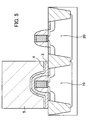
- FIG. 5 is a schematic cross-sectional view of an essential part of a tensile stress film etching step.
- FIG. 6 is a schematic cross-sectional view of an essential part of a UV irradiation step.
- FIG. 7 is a schematic cross-sectional view of an essential part of a compressive stress film deposition step.
- FIG. 8 is a schematic cross-sectional view of an essential part of a compressive stress film etching step.
- FIG. 9 is a schematic cross-sectional view of an essential part of an interlayer insulating film deposition step.
- FIG. 10 is a schematic cross-sectional view of an essential part of a UV irradiation step to a tensile stress film and a compressive stress film.
- FIG. 1 is a schematic cross-sectional view of an essential part of a MOSFET formation step.
- a basic CMOS structure having an n-MOSFET 10 and a p-MOSFET 20 as shown in FIG. 1 is first formed according to a normal process.
- the CMOS structure is, formed, for example, using a p-type Si substrate 1 .
- the n-MOSFET 10 and the p-MOSFET 20 are subjected to element isolation by a Shallow Trench Isolation (STI) 2 .
- STI Shallow Trench Isolation
- the n-MOSFET 10 is formed as follows.
- a p-type well region 11 is formed, for example, using a p-type impurity such as boron (B).
- a gate electrode 13 made of polysilicon is formed through a gate insulating film 12 made of silicon oxide (SiO 2 ).
- a sidewall 14 made of SiO 2 is formed.
- a source drain extension region 15 and a source drain region 16 are formed using an n-type impurity such as phosphorus (P) or arsenic (As).
- silicide layers 17 are formed on a surface layer of the gate electrode 13 as well as on a surface layer of the source drain region 16 .
- No well region 11 may be formed within the Si substrate 1 of the n-MOSFET 10 .
- the p-MOSFET 20 is formed as follows. Within the Si substrate 1 for forming the p-MOSFET 20 , an n-type well region 21 is formed, for example, using P or As. On such an Si substrate 1 , a gate electrode 23 made of polysilicon is formed through a gate insulating film 22 made of silicon oxide (SiO 2 ). On side walls of the gate insulating film 22 and the gate electrode 23 , a sidewall 24 made of SiO 2 is formed. Within the Si substrate 1 on both sides of the gate electrode 23 , a source drain extension region 25 and a source drain region 26 are formed using a p-type impurity such as B. On a surface layer of the gate electrode 23 as well as on a surface layer of the source drain region 26 , silicide layers 27 are formed.
- the CMOS structure (substrate) including the n-MOSFET 10 and p-MOSFET 20 each having the above-described structure is formed according to a normal process.
- a film thickness and impurity concentration of each portion in this CMOS structure are arbitrarily set in response to demand characteristics of the CMOS structure.
- the gate electrodes 13 and 23 are each formed to a gate length of about 30 to 40 nm and a gate height of about 100 nm.
- the sidewalls 14 and 24 are each formed to a width of about 50 nm.
- FIG. 2 is a schematic cross-sectional view of an essential part of a tensile stress film deposition step.
- a tensile stress film 3 made of SiN and having a film thickness of about 70 nm is deposited over the whole surface of the substrate.
- the tensile stress film 3 is deposited, for example, using a Chemical Vapor Deposition (CVD) method.
- CVD Chemical Vapor Deposition
- silane gas SiH 2 Cl 2 , SiH 4 , Si 2 H 4 , Si 2 H 6
- NH 3 ammonia
- a flow rate of the silane gas is set in the range of 5 to 50 sccm and a flow rate of the NH 3 gas is set in the range of 500 to 10000 sccm.
- nitrogen gas (N 2 ) or argon (Ar) gas is used as a carrier gas and a flow rate thereof is set in the range of 500 to 10000 sccm.
- a chamber for introducing each gas is controlled to have an inner pressure of 0.1 to 400 Torr and a temperature of 400° C. to 450° C.
- the flow rate unit sccm is a reduced value of the flow rate mL/min at 0° C. and 101.3 kPa. 1 Torr is about 133.322 Pa.
- the tensile stress film 3 deposited under such conditions has a tensile stress of about 400 to 500 MPa.
- hydrogen (H) usually remains.
- the process proceeds to the next step without performing the UV irradiation to the film 3 .
- FIG. 3 is a schematic cross-sectional view of an essential part of an oxide film deposition step.
- a SiO 2 film 4 is deposited on the film 3 .
- the SiO 2 film 4 is deposited to a film thickness of about 25 nm, for example, using a plasma CVD method.
- a mixed gas composed of SiH 4 and oxygen (O 2 ) is used and a substrate temperature is set to about 400° C.
- the SiO 2 film 4 herein formed functions as an etching stopper in etching the after-mentioned compressive stress film 6 (see FIG. 8 ).
- FIG. 4 is a schematic cross-sectional view of an essential part of an oxide film etching step.
- a resist mask 5 is formed on the n-MOSFET 10 side and the SiO 2 film 4 deposited on the p-MOSFET 20 side is removed by etching.
- the etching of the SiO 2 film 4 is performed, for example, by a Reactive Ion Etching (RIE) method using a C 4 F 8 /Ar/O 2 gas.
- RIE Reactive Ion Etching
- FIG. 5 is a schematic cross-sectional view of an essential part of a tensile stress film etching step.
- the tensile stress film 3 deposited on the p-MOSFET 20 side is removed by etching using the same resist mask 5 .
- the etching of the film 3 is performed, for example, by the RIE method using a CHF 3 /Ar/O 2 gas.
- the resist mask 5 is removed.
- the tensile stress film 3 and the SiO 2 film 4 are left only on the n-MOSFET 10 .
- a tensile stress is applied by this tensile stress film 3 .
- FIG. 6 is a schematic cross-sectional view of an essential part of a UV irradiation step.
- UV irradiation is performed to the tensile stress film 3 which remains on the n-MOSFET 10 .
- the UV irradiation is performed, for example, under conditions where the irradiation temperature is about 450° C. and the irradiation time is about 20 minutes.
- the irradiated UV transmits the thin SiO 2 film 4 to reach the tensile stress film 3 under the film 4 .
- the tensile stress film 3 irradiated with UV is increased in the tensile stress as well as is cured as compared with that before the UV irradiation. This results from the fact that hydrogen which remains in the tensile stress film 3 is removed by the UV irradiation.
- the tensile stress which is about from 400 to 500 MPa before the UV irradiation can be improved to about 2 GPa.
- the UV irradiation to the tensile stress film 3 may be performed over the whole surface of the film 3 after the deposition of the film 3 over the whole surface of the substrate shown in FIG. 2 .
- the removal by etching of the film 3 is made easy and at the same time, an improvement of the tensile stress can be attained.
- the UV irradiation is performed, for example, under conditions where the irradiation temperature is about 450° C. and the irradiation time is about 25 minutes.
- the irradiation temperature is about 450° C.
- the irradiation time is about 25 minutes.
- UV irradiation step shown in FIG. 6 UV is irradiated not only to the tensile stress film 3 which remains on the n-MOSFET 10 but also to the p-MOSFET 20 which is exposed by the removal of the film 3 in the step shown in FIG. 5 .
- no characteristic deterioration of the p-MOSFET 20 due to this UV irradiation is recognized. Accordingly, by performing the UV irradiation, an improvement in the tensile stress of the film 3 which remains on the n-MOSFET 10 can be attained without exerting any influence on the p-MOSFET 20 .
- a sidewall of a MOSFET is generally formed using SiO 2 or SiN.
- the sidewalls 14 and 24 are preferably formed using SiO 2 as described above. The reason is that in the UV irradiation step shown in FIG. 6 , UV is irradiated not only to the tensile stress film 3 on the n-MOSFET 10 but also to the sidewall 14 of the n-MOSFET 10 or to the sidewall 24 of the p-MOSFET 20 .
- a tensile stress may occur on the sidewalls due to the UV irradiation, depending on the composition of the sidewalls.
- the tensile stress occurs on the sidewall 14 of the n-MOSFET 10
- the tensile stress is applied to a channel region of the n-MOSFET 10 from the tensile stress film 3 as well as from the sidewall 14 .
- FIG. 7 is a schematic cross-sectional view of an essential part of a compressive stress film deposition step.
- the compressive stress film 6 made of SiN and having a film thickness of about 70 nm is deposited over the whole surface of the substrate where the film 3 and the SiO 2 film 4 remain.
- the compressive stress film 6 is deposited, for example, using the CVD method.
- SiH 4 gas is used as an Si material and NH 3 gas is used as an N material.
- a flow rate of the SiH 4 gas is set in the range of 100 to 1000 sccm and a flow rate of the NH 3 gas is set in the range of 500 to 10000 sccm.
- nitrogen (N 2 ) gas or argon (Ar) gas is used as a carrier gas and the flow rate thereof is set in the range of 500 to 10000 sccm.
- a chamber for introducing each gas is controlled to have an inner pressure of 0.1 to 400 Torr and a temperature of 400 to 450° C.
- RF power is about 100 to 1000 W.
- the compressive stress film 6 deposited under such conditions has a compressive stress of about 3 GPa.
- FIG. 8 is a schematic cross-sectional view of an essential part of a compressive stress film etching step.
- a resist mask 7 is formed on the p-MOSFET 20 side.
- the compressive stress film 6 deposited on the n-MOSFET 10 side is removed by etching.
- the etching of the compressive stress film 6 is performed, for example, by the RIE method using a CHF 3 /Ar/O 2 gas.
- the resist mask 7 is removed.
- FIG. 9 is a schematic cross-sectional view of an essential part of an interlayer insulating film deposition step.
- a TEOS oxide film 8 as an interlayer insulating film is deposited over the whole surface.
- TEOS tetra-ethoxysilane
- Si(OC 2 H 5 OH) 4 tetra-ethoxysilane
- the TEOS oxide film 8 is deposited using the plasma CVD method.
- the TEOS oxide film 8 is first deposited over the whole surface to a film thickness of about 600 nm.
- the film 8 is flattened using a Chemical Mechanical Polishing (CMP) method and finally reduced to a film thickness of about 350 nm.
- CMP Chemical Mechanical Polishing
- CMOS structure in which the tensile stress film 3 and the compressive stress film 6 are split and stuck on the n-MOSFET 10 and the p-MOSFET 20 , respectively. Thereafter, a contact electrode and a wiring layer are formed according to a normal process. Thus, a device having the CMOS structure is completed.
- the tensile stress film 3 is formed over the whole surface. Then, the film 3 is removed by etching from the p-MOSFET 20 surface while being left on the n-MOSFET 10 . Further, UV irradiation is performed to the remaining film 3 . Thereafter, the compressive stress film 6 is formed on the p-MOSFET 20 .
- the etching of the tensile stress film 3 is performed with ease and with high accuracy as well as the tensile stress film 3 having a large tensile stress can be formed on the n-MOSFET 10 . Accordingly, there can be realized a high-performance and high-quality CMOS device in which a large tensile stress is applied to the channel region of the n-MOSFET 10 and a large compressive stress is applied to the channel region of the p-MOSFET 20 .
- the UV irradiation to the tensile stress film 3 removes hydrogen which remains in the film as described above. Accompanying with the removal, a tensile stress of the film 3 is improved and as a result, an improvement in an electron mobility in the n-MOSFET 10 is attained. Further, by the removal of hydrogen from the tensile stress film 3 , Negative Bias Temperature Instability (NBTI) in the CMOS device may be suppressed.
- NBTI Negative Bias Temperature Instability
- the second embodiment differs from the first embodiment in the following point.
- the tensile stress film 3 and the compressive stress film 6 are formed on the n-MOSFET 10 and the p-MOSFET 20 , respectively. Then, UV irradiation is collectively performed to both of the tensile stress film 3 and the compressive stress film 6 .
- deposition of the tensile stress film 3 shown in FIG. 2 formation and etching of the SiO 2 film 4 shown in FIGS. 3 and 4 , and etching of the tensile stress film 3 shown in FIG. 5 are performed on the CMOS structure shown in FIG. 1 .
- the process proceeds to the deposition step of the compressive stress film 6 shown in FIG. 7 .
- the film 6 on the film 4 is removed by etching and then, a resist mask 7 is removed as shown in FIG. 8 .
- UV irradiation is performed to the films 3 and 6 .
- FIG. 10 is a schematic cross-sectional view of an essential part of a UV irradiation step to a tensile stress film and a compressive stress film.
- UV irradiation is collectively performed to both of the tensile stress film 3 and the compressive stress film 6 .
- the UV irradiation is performed for example, under conditions where the irradiation temperature is about 450° C. and the irradiation time is about 20 minutes.
- the tensile stress in the film 3 which is about from 400 to 500 MPa before the UV irradiation, can be improved to about 2 GPa.
- UV irradiation UV is irradiated to the tensile stress film 3 as well as to the compressive stress film 6 .
- the UV irradiation to the compressive stress film 6 leads to reduction in the compressive stress.
- the amount of reduction in the compressive stress due to UV irradiation can be suppressed to 200 MPa or less (the compressive stress in the film 6 before the UV irradiation is about 3 GPa).
- the TEOS oxide film 8 having a predetermined film thickness is formed as shown in FIG. 9 .
- the CMOS structure in which the tensile stress film 3 and the compressive stress film 6 are split and stuck on the n-MOSFET 10 and the p-MOSFET 20 , respectively.
- a contact electrode and a wiring layer are formed according to a normal process.
- a device having the CMOS structure is completed.
- the tensile stress film 3 is first deposited over the whole surface. Then, the film 3 deposited on the p-MOSFET 20 side is removed by etching so as to be left on the n-MOSFET 10 . Thereafter, the compressive stress film 6 is deposited over the whole surface. Then, the film 6 deposited on the n-MOSFET 10 side is removed by etching so as to be left on the p-MOSFET 20 .
- a deposition order of the tensile stress film 3 and the compressive stress film 6 may be reversed. More specifically, the compressive stress film 6 is first deposited over the whole surface. Then, the film 6 deposited on the n-MOSFET 10 side is removed by etching so as to be left on the p-MOSFET 20 . Thereafter, the tensile stress film 3 is deposited over the whole surface. Then, the film 3 deposited on the p-MOSFET 20 side is removed by etching so as to be left on the n-MOSFET 10 .
- UV irradiation under the predetermined conditions may be collectively performed to the tensile stress film 3 and the compressive stress film 6 .
- the UV irradiation is collectively performed to the films 3 and 6 .
- the etching of the tensile stress film 3 is performed with ease and with high accuracy as well as the tensile stress film 3 having a large tensile stress can be formed on the n-MOSFET 10 . Further, the tensile stress of the compressive stress film 6 is kept large even after the UV irradiation. Accordingly, there can be realized a high-performance and high-quality CMOS device in which a large tensile stress is applied to the channel region of the n-MOSFET 10 and a large compressive stress is applied to the channel region of the p-MOSFET 20 .
- the collective UV irradiation to the tensile stress film 3 and the compressive stress film 6 removes hydrogen which remains in the films 3 and 6 , as described above.
- the NBTI in the CMOS device may be suppressed.
- the splitting and sticking process of the tensile stress film and the compressive stress film in the CMOS structure is described by way of example.
- the above-described method for performing the UV irradiation to the tensile stress film after completion of the etching can be similarly applied to a forming process of the CMOS device as well as of various devices having an n-MOSFET.
- a method for depositing over the whole surface of the substrate having formed thereon the n-MOSFET the tensile stress film having the tensile stress may be employed, removing by etching the film while leaving it on the n-MOSFET, and performing UV irradiation to the tensile stress film which remains on the n-MOSFET.
- the tensile stress film having a certain level of tensile stress is previously deposited on the n-MOSFET. Then, UV irradiation is performed to the tensile stress film to increase the tensile stress of the film.
- a method for depositing the compressive stress film having a certain level of compressive stress and performing UV irradiation to the film to produce the compressive stress may be employed, for example, a method for depositing the compressive stress film having a certain level of compressive stress and performing UV irradiation to the film to produce the compressive stress.
- the stress film is formed on the substrate having formed thereon a transistor, the stress film is removed while being left on the transistor and then, UV irradiation is performed to the remaining stress film. Therefore, removal of the stress film can be performed with high accuracy. As a result, there can be realized the high-performance and high-quality semiconductor device having a transistor in which the carrier mobility is improved by the stress film.
Landscapes
- Insulated Gate Type Field-Effect Transistor (AREA)
- Metal-Oxide And Bipolar Metal-Oxide Semiconductor Integrated Circuits (AREA)
- Electrodes Of Semiconductors (AREA)
- Formation Of Insulating Films (AREA)
Abstract
Description
Claims (4)
Applications Claiming Priority (2)
| Application Number | Priority Date | Filing Date | Title |
|---|---|---|---|
| JP2006-215405 | 2006-08-08 | ||
| JP2006215405A JP5017958B2 (en) | 2006-08-08 | 2006-08-08 | Manufacturing method of semiconductor device |
Publications (2)
| Publication Number | Publication Date |
|---|---|
| US20080124856A1 US20080124856A1 (en) | 2008-05-29 |
| US7763509B2 true US7763509B2 (en) | 2010-07-27 |
Family
ID=39176658
Family Applications (1)
| Application Number | Title | Priority Date | Filing Date |
|---|---|---|---|
| US11/639,344 Expired - Fee Related US7763509B2 (en) | 2006-08-08 | 2006-12-15 | Method of manufacturing semiconductor device including forming two stress films and irradiation of one stress film |
Country Status (2)
| Country | Link |
|---|---|
| US (1) | US7763509B2 (en) |
| JP (1) | JP5017958B2 (en) |
Cited By (4)
| Publication number | Priority date | Publication date | Assignee | Title |
|---|---|---|---|---|
| US20090302391A1 (en) * | 2008-06-05 | 2009-12-10 | Chartered Semiconductor Manufacturing, Ltd. | Stress liner for stress engineering |
| US20100167533A1 (en) * | 2008-12-26 | 2010-07-01 | Samsung Electronics Co., Ltd. | Method of fabricating semiconductor integrated circuit device |
| US20120161242A1 (en) * | 2010-12-22 | 2012-06-28 | Globalfoundries Inc. | Enhancement of ultraviolet curing of tensile stress liner using reflective materials |
| US9899386B2 (en) * | 2004-03-30 | 2018-02-20 | Samsung Electronics Co., Ltd. | Low noise and high performance LSI device |
Families Citing this family (7)
| Publication number | Priority date | Publication date | Assignee | Title |
|---|---|---|---|---|
| US20080169510A1 (en) * | 2007-01-17 | 2008-07-17 | International Business Machines Corporation | Performance enhancement on both nmosfet and pmosfet using self-aligned dual stressed films |
| JP5064289B2 (en) * | 2008-04-17 | 2012-10-31 | パナソニック株式会社 | Semiconductor device and manufacturing method thereof |
| CN102646637A (en) * | 2011-02-17 | 2012-08-22 | 中芯国际集成电路制造(上海)有限公司 | CMOS (complementary metal oxide semiconductor) device and forming method thereof |
| US8293605B2 (en) * | 2011-02-25 | 2012-10-23 | GlobalFoundries, Inc. | Methods for fabricating a CMOS integrated circuit having a dual stress layer (DSL) |
| CN103378004B (en) * | 2012-04-23 | 2015-11-25 | 中芯国际集成电路制造(上海)有限公司 | One has the tectal cmos device manufacture method of stress |
| CN102709179B (en) * | 2012-06-21 | 2015-03-11 | 上海华力微电子有限公司 | Forming method of dual-stress silicon nitride etched block layer and manufacturing method of semiconductor device |
| CN110459465B (en) * | 2019-08-30 | 2022-03-04 | 上海华力微电子有限公司 | Method for forming self-aligned double-layer pattern |
Citations (4)
| Publication number | Priority date | Publication date | Assignee | Title |
|---|---|---|---|---|
| JP2005057301A (en) | 2000-12-08 | 2005-03-03 | Renesas Technology Corp | Semiconductor device and method of manufacturing same |
| US20060160314A1 (en) * | 2005-01-15 | 2006-07-20 | Applied Materials, Inc. | Substrate having silicon germanium material and stressed silicon nitride layer |
| US20070105299A1 (en) * | 2005-11-10 | 2007-05-10 | International Business Machines Corporation | Dual stress memory technique method and related structure |
| US7232730B2 (en) * | 2005-04-29 | 2007-06-19 | Taiwan Semiconductor Manufacturing Company, Ltd. | Method of forming a locally strained transistor |
Family Cites Families (7)
| Publication number | Priority date | Publication date | Assignee | Title |
|---|---|---|---|---|
| US7053400B2 (en) * | 2004-05-05 | 2006-05-30 | Advanced Micro Devices, Inc. | Semiconductor device based on Si-Ge with high stress liner for enhanced channel carrier mobility |
| US7265066B2 (en) * | 2005-03-29 | 2007-09-04 | Tokyo Electron, Ltd. | Method and system for increasing tensile stress in a thin film using collimated electromagnetic radiation |
| JP2007200961A (en) * | 2006-01-24 | 2007-08-09 | Sharp Corp | Semiconductor device and manufacturing method thereof |
| JP2007208079A (en) * | 2006-02-02 | 2007-08-16 | Nec Electronics Corp | Semiconductor device and manufacturing method thereof |
| KR100703986B1 (en) * | 2006-05-22 | 2007-04-09 | 삼성전자주식회사 | Semiconductor device having analog transistor with improved operation characteristics and flicker noise characteristics, and manufacturing method thereof |
| JP2007324391A (en) * | 2006-06-01 | 2007-12-13 | Matsushita Electric Ind Co Ltd | Semiconductor device and manufacturing method thereof |
| JP2008016569A (en) * | 2006-07-04 | 2008-01-24 | Sharp Corp | Semiconductor device and manufacturing method thereof |
-
2006
- 2006-08-08 JP JP2006215405A patent/JP5017958B2/en not_active Expired - Fee Related
- 2006-12-15 US US11/639,344 patent/US7763509B2/en not_active Expired - Fee Related
Patent Citations (4)
| Publication number | Priority date | Publication date | Assignee | Title |
|---|---|---|---|---|
| JP2005057301A (en) | 2000-12-08 | 2005-03-03 | Renesas Technology Corp | Semiconductor device and method of manufacturing same |
| US20060160314A1 (en) * | 2005-01-15 | 2006-07-20 | Applied Materials, Inc. | Substrate having silicon germanium material and stressed silicon nitride layer |
| US7232730B2 (en) * | 2005-04-29 | 2007-06-19 | Taiwan Semiconductor Manufacturing Company, Ltd. | Method of forming a locally strained transistor |
| US20070105299A1 (en) * | 2005-11-10 | 2007-05-10 | International Business Machines Corporation | Dual stress memory technique method and related structure |
Cited By (7)
| Publication number | Priority date | Publication date | Assignee | Title |
|---|---|---|---|---|
| US9899386B2 (en) * | 2004-03-30 | 2018-02-20 | Samsung Electronics Co., Ltd. | Low noise and high performance LSI device |
| US20090302391A1 (en) * | 2008-06-05 | 2009-12-10 | Chartered Semiconductor Manufacturing, Ltd. | Stress liner for stress engineering |
| US8999863B2 (en) * | 2008-06-05 | 2015-04-07 | Globalfoundries Singapore Pte. Ltd. | Stress liner for stress engineering |
| US20100167533A1 (en) * | 2008-12-26 | 2010-07-01 | Samsung Electronics Co., Ltd. | Method of fabricating semiconductor integrated circuit device |
| US8227308B2 (en) * | 2008-12-26 | 2012-07-24 | Samsung Electronics Co., Ltd. | Method of fabricating semiconductor integrated circuit device |
| US20120161242A1 (en) * | 2010-12-22 | 2012-06-28 | Globalfoundries Inc. | Enhancement of ultraviolet curing of tensile stress liner using reflective materials |
| US8435841B2 (en) * | 2010-12-22 | 2013-05-07 | GlobalFoundries, Inc. | Enhancement of ultraviolet curing of tensile stress liner using reflective materials |
Also Published As
| Publication number | Publication date |
|---|---|
| JP2008041981A (en) | 2008-02-21 |
| US20080124856A1 (en) | 2008-05-29 |
| JP5017958B2 (en) | 2012-09-05 |
Similar Documents
| Publication | Publication Date | Title |
|---|---|---|
| US7205206B2 (en) | Method of fabricating mobility enhanced CMOS devices | |
| US7785950B2 (en) | Dual stress memory technique method and related structure | |
| US7592231B2 (en) | MOS transistor and fabrication thereof | |
| US8324038B2 (en) | Method of removing a spacer, method of manufacturing a metal-oxide-semiconductor transistor device, and metal-oxide-semiconductor transistor device | |
| US7494884B2 (en) | SiGe selective growth without a hard mask | |
| US7655987B2 (en) | Method for fabricating ultra-high tensile-stressed film and strained-silicon transistors thereof | |
| US7777284B2 (en) | Metal-oxide-semiconductor transistor and method of forming the same | |
| US7612389B2 (en) | Embedded SiGe stressor with tensile strain for NMOS current enhancement | |
| US8809141B2 (en) | High performance CMOS transistors using PMD liner stress | |
| US9196475B2 (en) | Methods for fabricating integrated circuits including fluorine incorporation | |
| KR20110123733A (en) | Method of fabricating MOS devices having epitaxially grown stress-induced source and drain regions | |
| US7763509B2 (en) | Method of manufacturing semiconductor device including forming two stress films and irradiation of one stress film | |
| CN106298527A (en) | Pmos transistor and forming method thereof | |
| US20100012992A1 (en) | Method of manufacturing semiconductor device | |
| US7977194B2 (en) | Method for fabricating semiconductor device with fully silicided gate electrode | |
| US20060172556A1 (en) | Semiconductor device having a high carbon content strain inducing film and a method of manufacture therefor | |
| US20070093032A1 (en) | Method of manufacturing semiconductor device | |
| US7675118B2 (en) | Semiconductor structure with enhanced performance using a simplified dual stress liner configuration | |
| US7629271B1 (en) | High stress diamond like carbon film | |
| US20110008938A1 (en) | Thin film and method for manufacturing semiconductor device using the thin film | |
| US20080237748A1 (en) | Method for fabricating high compressive stress film and strained-silicon transistors | |
| CN101320691A (en) | Method for manufacturing metal oxide semiconductor transistor | |
| CN100536087C (en) | Method for manufacturing compressive nitride layer and method for forming transistor | |
| JP2009302175A (en) | Method of manufacturing semiconductor device |
Legal Events
| Date | Code | Title | Description |
|---|---|---|---|
| AS | Assignment |
Owner name: FUJITSU LIMITED, JAPAN Free format text: ASSIGNMENT OF ASSIGNORS INTEREST;ASSIGNORS:PIDIN, SERGEY;OWADA, TAMOTSU;REEL/FRAME:018715/0495 Effective date: 20061010 |
|
| AS | Assignment |
Owner name: FUJITSU MICROELECTRONICS LIMITED, JAPAN Free format text: ASSIGNMENT OF ASSIGNORS INTEREST;ASSIGNOR:FUJITSU LIMITED;REEL/FRAME:021976/0089 Effective date: 20081104 Owner name: FUJITSU MICROELECTRONICS LIMITED,JAPAN Free format text: ASSIGNMENT OF ASSIGNORS INTEREST;ASSIGNOR:FUJITSU LIMITED;REEL/FRAME:021976/0089 Effective date: 20081104 |
|
| STCF | Information on status: patent grant |
Free format text: PATENTED CASE |
|
| AS | Assignment |
Owner name: FUJITSU SEMICONDUCTOR LIMITED, JAPAN Free format text: CHANGE OF NAME;ASSIGNOR:FUJITSU MICROELECTRONICS LIMITED;REEL/FRAME:024651/0744 Effective date: 20100401 |
|
| FEPP | Fee payment procedure |
Free format text: PAYOR NUMBER ASSIGNED (ORIGINAL EVENT CODE: ASPN); ENTITY STATUS OF PATENT OWNER: LARGE ENTITY |
|
| FPAY | Fee payment |
Year of fee payment: 4 |
|
| AS | Assignment |
Owner name: FUJITSU SEMICONDUCTOR LIMITED, JAPAN Free format text: CHANGE OF ADDRESS;ASSIGNOR:FUJITSU SEMICONDUCTOR LIMITED;REEL/FRAME:041188/0401 Effective date: 20160909 |
|
| MAFP | Maintenance fee payment |
Free format text: PAYMENT OF MAINTENANCE FEE, 8TH YEAR, LARGE ENTITY (ORIGINAL EVENT CODE: M1552) Year of fee payment: 8 |
|
| FEPP | Fee payment procedure |
Free format text: MAINTENANCE FEE REMINDER MAILED (ORIGINAL EVENT CODE: REM.); ENTITY STATUS OF PATENT OWNER: LARGE ENTITY |
|
| LAPS | Lapse for failure to pay maintenance fees |
Free format text: PATENT EXPIRED FOR FAILURE TO PAY MAINTENANCE FEES (ORIGINAL EVENT CODE: EXP.); ENTITY STATUS OF PATENT OWNER: LARGE ENTITY |
|
| STCH | Information on status: patent discontinuation |
Free format text: PATENT EXPIRED DUE TO NONPAYMENT OF MAINTENANCE FEES UNDER 37 CFR 1.362 |
|
| FP | Lapsed due to failure to pay maintenance fee |
Effective date: 20220727 |