US7755448B2 - Differential impedance matching circuit and method with harmonic suppression - Google Patents
Differential impedance matching circuit and method with harmonic suppression Download PDFInfo
- Publication number
- US7755448B2 US7755448B2 US11/970,237 US97023708A US7755448B2 US 7755448 B2 US7755448 B2 US 7755448B2 US 97023708 A US97023708 A US 97023708A US 7755448 B2 US7755448 B2 US 7755448B2
- Authority
- US
- United States
- Prior art keywords
- node
- differential input
- harmonic
- circuit
- differential
- Prior art date
- Legal status (The legal status is an assumption and is not a legal conclusion. Google has not performed a legal analysis and makes no representation as to the accuracy of the status listed.)
- Active, expires
Links
Images


Classifications
-
- H—ELECTRICITY
- H03—ELECTRONIC CIRCUITRY
- H03H—IMPEDANCE NETWORKS, e.g. RESONANT CIRCUITS; RESONATORS
- H03H7/00—Multiple-port networks comprising only passive electrical elements as network components
- H03H7/38—Impedance-matching networks
Definitions
- This invention pertains to impedance matching for power amplifiers and, more specifically, baluns circuits.
- Baluns circuits are used to make a balanced to unbalanced transformation, for impedance matching between the balanced and unbalanced ports, and also suppress the common mode signal at the balanced ports at the 2 nd harmonic frequency.
- FIG. 2 One example of a widely known conventional solution (utilized by Chipcon AS of Norway as well) is illustrated in FIG. 2 .
- LC resonant circuits at the two signal paths of the differential outputs/inputs (O 1 b 58 and O 2 b 60 ) shift +90 and ⁇ 90 degrees at the fundamental frequency and thus sum the two signal paths in phase at the single ended output 72 .
- the matching network is typically difficult to design if a parallel parasitic impedance is present between the differential outputs/inputs, e.g. a transmitter (TX) or receiver (RX) with parallel parasitic RC.
- TX transmitter
- RX receiver
- the network should present an optimum antenna impedance at the differential inputs (O 1 b 58 and O 2 b 60 ) in order to deliver maximum power to the unbalanced port 72 in Tx mode or in a reverse way in Rx mode.
- This optimum antenna impedance has a reactance (usually inductive) that resonates with the TX or RX reactance (usually capacitive) at the operating frequency.
- the impedance also has a real part that must be properly adjusted to obtain a voltage swing between the differential inputs up to the allowed maximum or if the voltage swing is not maximized to produce a conjugate matched termination for the TX or RX.
- This matching network operates well only near to the series resonant frequency of it's LC (L 1 62 , C 1 64 ) and CL (C 2 66 , L 2 70 ) arms.
- the network shows a high impedance between its differential inputs (O 1 b 58 and O 2 b 60 ) so that the generation of the optimum antenna impedance is difficult if not impossible.
- the circuit uses the series parasitic inductances of the transistors with external capacitors. Also, the 2 nd harmonic suppression and the balun operation (coil balun) are realized with different circuit blocks, which adds cost to the circuit.
- the solution of Fisher may be applied in the case of transistors with series parasitic output inductance, but is generally not applicable to differential transmitters with parallel parasitic capacitances. Also, the differential transmitter outputs are not matched to the coil balun inputs at the fundamental frequency, which causes losses that reduce power transfer.
- balun circuit is found in U.S. Pat. No. 7,034,630 for a “Balun transformer and transceiver”.
- a balun circuit is described that achieves the balanced-unbalanced transformation by using coupled transmission line elements. It also includes two resonant circuits: one at the single ended and one at the differential side. They generate a band pass filter characteristic at the fundamental frequency.
- One embodiment of a matching network having first 10 and second 12 differential input nodes and a single ended output node 30 includes a first inductor L 11 16 coupled between the first differential input node 10 and a common circuit node 28 and a second inductor L 12 18 coupled between the second differential input node 12 and the common circuit node 28 .
- a third inductor L DC 14 is coupled between a first power supply rail Vcc and the common circuit node 28 .
- a first capacitor C 1 22 is coupled between the first differential input node 10 and the single ended output node 30 .
- a second capacitor C 2 26 is coupled between the second differential input node 12 and a good Rf ground (which can be even a power supply rail or any other node if it is a good RF ground).
- a fourth inductor L 2 24 is coupled between the second differential input node 12 and the single ended output node 30 .
- a third capacitor C 3 20 is coupled between the common circuit node 28 and a good Rf ground (which can be even a power supply rail or any other node if it is a good RF ground) such that the third capacitor C 3 20 provides second harmonic suppression of a common mode signal present at the first 10 and second 12 differential input nodes.
- the values of the first C 1 22 and second C 2 26 capacitors and the first L 11 16 , second L 12 18 and fourth L 2 24 inductors are selected for operation at a predetermined fundamental frequency.
- the value of the third capacitor C 3 20 is selected to provide a low impedance path to a good RF ground for the common mode signal at a second harmonic frequency.
- An embodiment of an inductive matching network includes first 358 and second 360 differential input nodes and a single ended output node 378 .
- a first inductor L DC1 370 is coupled between the first differential input node and a first power supply rail Vcc and a second inductor L 2 376 is coupled between the second differential input node and the single ended output node.
- a third inductor L 3 312 is coupled between a radio frequency ground node and a common circuit node 364 , where an inductance of the third inductor is selected to provide second harmonic suppression of a common mode signal present at the first and second differential input nodes.
- a fourth inductor L DC2 374 is coupled between the second differential input node and the first power supply rail Vcc.
- a first capacitor C 11 366 is coupled between the first differential input node and the common circuit node 364
- a second capacitor C 12 368 is coupled between the second differential input node and the common circuit node
- a third capacitor C 1 372 is coupled between the first differential input node and the single ended output node.
- the method calls for impedance matching first and second differential input nodes to a single ended output node using a first reactive impedance selected to pass a resonant frequency.
- the method also sets forth suppressing a harmonic frequency of a common mode signal presented at the first and second differential input nodes by providing a series resonance from the first and second differential input nodes to a radio frequency ground potential, where the series resonance is selected to pass the harmonic frequency to the radio frequency ground potential.
- FIG. 1 is a circuit diagram illustrating one exemplary embodiment of a matching network in accordance with the present invention
- FIG. 2 is a circuit diagram illustrating one example of a conventional matching network
- FIG. 3 is a graph that shows the simulated magnitudes and phases on the differential outputs O 1 b and O 2 b in FIG. 2 after several optimization cycles using a conventional optimization algorithm;
- FIG. 4 is a graph that shows the S 11 of the circuit of FIG. 2 ;
- FIG. 5 is a graph illustrating the voltages at the differential side (O 1 b 58 , O 2 b 60 ) of the circuit of FIG. 2 if the resistor R TX 56 is put back;
- FIG. 6 is a graph illustrating the fundamental output power of the circuit of FIG. 2 ;
- FIG. 7 is a graph illustrating the operation of the matching network of FIG. 2 at the second harmonic frequency
- FIG. 8 is a graph that illustrates the response of the matching network of FIG. 2 with respect to the common mode second harmonic
- FIG. 9 is a circuit diagram of the model used for the common mode simulation of FIG. 8 , wherein one of the current generators 102 was reversed with respect to FIG. 2 ;
- FIG. 10 is a circuit diagram illustrating another example of a conventional matching network
- FIG. 11 is a frequency response graph illustrating the simulated magnitudes and phases on the differential IC outputs O 1 b 158 and O 2 b 160 in FIG. 10 ;
- FIG. 12 is a graph that shows the S 11 for the circuit of FIG. 10 ;
- FIG. 13 is a graph that illustrates the voltages at the differential outputs O 1 b and O 2 b of FIG. 10 if the R TX 154 is put back, the S-parameter port at the single ended side is deactivated and the current generators 150 , 152 at the differential side are activated;
- FIG. 14 is a frequency response graph that illustrates the fundamental power output for the circuit of FIG. 10 ;
- FIG. 15 is a graph illustrating the voltages at O 1 b 158 and O 2 b 160 voltages of the matching network of FIG. 10 at the second harmonic frequency;
- FIG. 16 is a graph illustrating the response at the common mode second harmonic for the matching network of FIG. 10 ;
- FIG. 17 is a circuit diagram of the model used for the common mode simulation of FIG. 16 , wherein one of the current generators 202 was reversed;
- FIG. 18 is another circuit diagram for an embodiment of a matching network according to the present invention.
- FIG. 19 is a frequency response graph that illustrates the fundamental power output for the circuit of FIG. 18 ;
- FIG. 20 shows the simulated voltage magnitude and phase on the differential outputs O 1 b 258 and O 2 b 260 in FIG. 18 when the transmit current generators 250 , 252 are active;
- FIG. 21 shows the response curve for the circuit of FIG. 18 at the 2 nd harmonic frequency (1736 GHz);
- FIG. 22 is a circuit diagram of the circuit of FIG. 18 with one of the current generators 302 reversed for the common mode simulation;
- FIG. 23 is a response curve illustrating the response of the circuit of FIG. 22 for the common mode 2 nd harmonic signal
- FIG. 24 is a response curve illustrating the response of the circuit of FIG. 22 for the common mode 2 nd harmonic signal when lossy elements are used in the simulation;
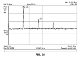
- FIG. 25 is a response curve illustrating the measured response of a circuit built and tested at 436 MHz showing the second and third harmonic with the common mode suppression capacitance 270 removed;
- FIG. 26 is a response curve illustrating the measure response of a circuit built and tested at 436 MHz showing the second and third harmonic with the common mode suppression capacitance 270 present.
- FIG. 27 is a circuit diagram of another exemplary embodiment of a circuit suitable for application to inductive output impedances.
- An embodiment of a circuit and method for a new matching balun network is described herein.
- One function of a matching network is to make a high impedance differential to single ended or unbalanced conversion and form a 2 nd harmonic trap at the input to suppress the second harmonic.
- TX transmitter
- R TX transmitter
- R TX receiver
- FIG. 1 One exemplary embodiment as applied to a transmitter (TX) chip model is a parallel RC. This embodiment is illustrated in FIG. 1 .
- the parallel equivalent resistance (R TX ) 6 depends on the transmitter Q.
- the concept may also be applied to a receiver (RX) matching baluns. In these embodiments, the jamming signals coming from the single ended side at the 2 nd harmonic frequency are suppressed.
- the embodiment of a baluns circuit shown in FIG. 1 has three basic operational functions.
- the circuit is designed to present an optimum differential antenna impedance to the TX at the fundamental frequency in order to obtain the available maximum level of power transfer from the transmitter to the matching networks differential inputs.
- This approach works well for conjugate complex matching applications, and also for applications wherein the voltage swing at the differential TX output is limited and thus the real part of the matching network admittance is much higher than the real part of the TX output admittance.
- the operation of the transmitter approaches an ideal current generator operation with high generator impedance and minimized internal loss.
- the embodiment of FIG. 1 also adds the two differential TX outputs in phase (for this the two out of phase differential outputs are summed in an out of phase way) at the fundamental frequency in order to increase power transfer at the 50 Ohm single ended output 30 . Due to the designed phase conditions (i.e. out of phase summation of the two transmit paths) for the differential signals, a common mode noise signal at the fundamental frequency is suppressed.
- the circuit of FIG. 1 also has a 2 nd harmonic trap, which is a series resonant circuit formed by the L 11 16 , L 12 18 inductances and the C 3 20 capacitor.
- This trap presents a short circuit to the common mode signal at the 2 nd harmonic frequency. Since the common mode signal is typically dominant at the 2 nd harmonic frequency for differential amplifiers, the trap obtains significant second harmonic suppression.
- the transmitter TX drives the balun in a differential mode (i.e. the two current generators 2 , 4 have identical direction).
- the common mode drive of the balun is illustrated in the embodiment of FIG. 22 , which shows a configuration in which the two current generators 300 , 302 are working in opposite direction.
- the value of capacitor value C 3 20 is selected to adjust the common mode trap at the second harmonic frequency.
- the behavior at the fundamental frequency can be designed separately from the 2 nd harmonic suppression trap. Both steps (especially the second one) require simple and short optimization efforts.
- FIG. 23 is a simulation output illustrating the common mode suppression both in the fundamental and the 2 nd harmonic frequency of the circuit in FIG. 22 .
- the power at the 50 Ohm output is simulated as if a pure common mode signal is presented at the differential inputs.
- the common mode suppression both at the fundamental and second harmonic is high.
- FIGS. 2 and 10 Three different matching network configurations that may be used for high impedance differential to single ended 50 Ohm transformation are analyzed below for comparison purposes. These networks are the conventional configurations of FIGS. 2 and 10 and an embodiment of the present invention shown in FIG. 1 .
- the elements used in the following simulation analysis of these matching networks are ideal loss free elements, since the purpose of this comparison is to illustrate the main effects on end behavior. A simulation with real lossy elements is not presented here.
- the elements are also modeled as linear devices, so simple AC analysis was used.
- the parallel equivalent resistance (R TX ) 6 in the transmitter model of FIG. 1 depends on the transmitter Q. With a typical 0.18 um CMOS technology, the Q is assumed to be 1.5 KOhm at 868 MHz.
- the parallel equivalent capacitance (C TX ) 8 is assumed to be 2 pF.
- the assumed targeted power is +20 dBm to the antenna.
- the assumed voltage magnitude on one output is assumed to be 2.5V. So the differential magnitude is 5V and, thus, the total peak to peak differential swing is 10V.
- the required current magnitude is 40 mA and the required equivalent parallel resulting resistance (e.g. the reciprocal of the real part of the so called optimum antenna admittance together with the parallel 1.5 KOhm of the TX) is 125 Ohm. From this, the reciprocal of the real part of the so called optimum antenna admittance should be 142 Ohm.
- the matching networks were configured to present this impedance to the transmitter output and also an inductive reactance, which is in resonance with the C TX 8 at 868 Mhz.
- the matching network of FIG. 2 yields some undesirable results. It is difficult to design even for acceptable fundamental operation, and also the resulting operation is not stable in case of technological spreading. It has no 2 nd harmonic suppression.
- the matching network of FIG. 10 is a modification of the network of FIG. 2 , which is easier to realize as no Vcc rail with good RF ground is required, easier to design as its characteristic is more suitable for differential operation at the fundamental frequency. However, no 2 nd harmonic suppression is achieved.
- the matching network of FIG. 1 provides many of the features of FIG. 10 , but includes an additional capacitance that provides strong suppression of the common mode at the second harmonic as well.
- the value of this capacitance can be designed easily for 2 nd harmonic suppression and also it is independent from the fundamental operation design.
- FIG. 3 is a graph that shows the simulated magnitudes 400 , 402 and phases 404 , 406 on the differential IC outputs (denoted by O 1 b 58 and O 2 b 60 in FIG. 2 ) after several optimization cycles using a conventional optimization algorithm.
- the result may not be optimum, but it was achieved after significant optimization effort, despite the simpler structure.
- the optimization has not adjusted the resonance of the circuit to 868 MHz.
- One reason may be that, at resonance, the impedance shown by the matching network at it's differential port is very high and thus no good matching to the optimum antenna impedance was possible to achieve.
- the optimization process adjusted the resonance to a lower frequency to achieve equal but lower voltage amplitudes and + ⁇ 90 degree phase shift with impedance matching at 868 Mhz. But it is not an optimum solution as the phase change vs. frequency is opposite at the two differential nodes. Thus, for example a technological variation which changes the resonant frequency will generate a big phase error i.e. the phase difference between the O 1 b 58 and O 2 b 60 voltages will strongly deviates from the desired 180 degree. It cause output power and common mode suppression degradation at the fundamental frequency.
- FIG. 4 is a graph that shows the S 11 of the circuit of FIG. 2 during the optimization. It has two minima. At resonance, the matching is poor, so if the single ended side is terminated by 50 Ohms, the matching network does not present the optimum antenna impedance at its differential port.
- the optimum equivalent parallel antenna resistance should be removed and the R TX 56 should be put back in the TX for a final simulation.
- the S 11 of the 50 Ohm single ended port may be less optimal as compared to the case when the matching network was forced to show the optimum antenna impedance between its differential inputs and now it is terminated with the TX impedance.
- FIG. 5 is a graph illustrating the voltages 420 , 422 at the differential side (O 1 b 58 , O 2 b 60 ) of the circuit of FIG. 2 if the resistor R TX 56 (1.5K) is put back.
- the S-parameter port at the single ended side 72 is deactivated and the current generators 52 , 54 at the differential side are activated (40 mA RF current magnitude).
- the resistance R TX 56 has influence on the phase and magnitude characteristic, but the quality of the operation is not improved.
- FIG. 6 is a graph illustrating the fundamental output power of the circuit of FIG. 2 .
- the graph shows that the output power is 14.7 dBm at 870 MHz, which is lower than the targeted +20 dBm due to improper operation.
- the power is much higher at 837 MHz where the resonance occurs, but, due to the non optimized conditions, it is far from the targeted +20 dBm.
- FIG. 7 is a graph illustrating the operation of the matching network of FIG. 2 at the second harmonic frequency, which is not optimal.
- the graph shows the O 1 b 58 and O 2 b 60 voltages 440 , 442 at the 2 nd harmonic frequency. Note that the observed magnitudes are far from equal and also that the phase difference is far from 180°.
- FIG. 8 shows that the matching network of FIG. 2 does not suppress the common mode second harmonic. This lack of suppression can also be observed in FIG. 8 , where the common mode suppression versus frequency is shown. Note that for the common mode simulation of FIG. 8 , one of the current generators 102 was reversed, as is illustrated in the circuit diagram of FIG. 9 .
- the common mode in the fundamental frequency is suppressed, but a sharp maximum is also found in close proximity to the fundamental frequency. This maximum is due to bad phase resonance conditions. So, in a case of element value spreading, even common mode gain can occur instead of suppression.
- the matching network of FIG. 2 is relatively difficult to design and optimize.
- the phase characteristic can be tuned to have nearly 180° difference, but it's frequency characteristic is not optimal for differential operation. It is unstable and sensitive to element value spreading.
- the targeted +20 dBm output power was not achieved in the simulation.
- the circuit does not adequately suppress the common mode at the 2 nd harmonic frequency.
- the common mode suppression and the output power at the fundamental frequency is very element sensitive.
- FIG. 11 is a frequency response graph illustrating the simulated magnitudes 460 , 462 and phases 464 , 466 on the differential IC outputs, which are denoted by O 1 b 158 and O 2 b 160 in FIG. 10 .
- the magnitudes are nearly equal and the phases are nearly +90° and ⁇ 90°. So the balun function is good.
- the phase difference is much more stable than in the previous cases as the phase characteristics of the two differential output voltages are parallel (i.e. the gradient has the same sign).
- FIG. 12 is a graph that shows the S 11 for the circuit of FIG. 10 . It has only one minima at the operation frequency, so that, if the single ended port 172 is terminated by 50 Ohm, the matching network will present a substantially optimum antenna impedance between its differential inputs.
- FIG. 13 is a graph that illustrates the voltages 480 , 482 at the differential side (O 1 b 158 , O 2 b 160 ) if the R TX 154 (1.5K) is put back, the S-parameter port at the single ended side 172 is deactivated and the current generators 150 , 152 at the differential side are activated (40 mA RF current magnitude). As can be seen in the graph, the magnitudes are nearly equal and the phase difference is also 180°. So the common mode suppression at the fundamental frequency is good and also the fundamental power is high. The simulation demonstrates that the circuit of FIG. 10 performs better at the fundamental frequency than the matching network of FIG. 2 .
- FIG. 14 is a frequency response graph that illustrates the fundamental power output for the circuit of FIG. 10 .
- the power output is only slightly lower than +20 dBm due to slight phase ( ⁇ 1°) and magnitude ( ⁇ 5 mV) errors.
- FIG. 15 is a graph illustrating that the performance of the matching network of FIG. 10 at the second harmonic frequency is non optimal.
- the graph shows the O 1 b and O 2 b voltages 500 , 502 at the 2 nd harmonic frequency. Note that the observed magnitudes are far from equal and also that the phase difference is far from 180°. Thus, the graph demonstrates that the matching network of FIG. 10 does not adequately suppress the common mode second harmonic. This poor suppression may also be observed in FIG. 16 , where the second harmonic suppression is shown.
- one of the current generators 152 of the circuit of FIG. 10 was reversed, as shown in FIG. 17 (generator 202 ).
- circuit of FIG. 10 is further optimized to second harmonic, improvement can be achieved, however, the result is still sub-optimal. Optimization for second harmonic suppression requires the addition of another element, which is discussed below with regard to the solution of FIG. 1 .
- the matching network of FIG. 10 is relatively easy to design and optimize for the fundamental.
- the phase characteristic can be tuned to have nearly 180° difference and it's frequency characteristic is substantially optimal for differential operation.
- the targeted +20 dBm output power was nearly achieved. Realization is also easier as no Vcc trail with good Rf ground properties is required.
- this matching network cannot adequately suppress the common mode at the 2 nd harmonic frequency.
- FIG. 18 a circuit diagram of the 868 MHz matching network with 2 nd harmonic suppression is shown in FIG. 18 . While the circuit of FIG. 18 is similar to the circuit of FIG. 10 , the inductor L 1 164 is effectively cut into two parts (denoted by L 11 266 and L 12 268 ) and the middle point 264 is connected to a radio frequency ground potential through capacitor C 3 270 . The function of capacitor C 3 270 is to form a series resonance together with the L 11 266 and L 12 268 inductors at the 2 nd harmonic frequency, and create a short circuit for the common mode, which is dominant at the 2 nd harmonic frequency. In this way, significant 2 nd harmonic suppression can be achieved.
- the design is simple to apply because the 2 nd harmonic suppression with capacitor C 3 270 can be designed independently of the fundamental behavior.
- the basic design procedure at the fundamental frequency is basically the same as it was for the circuit described above, e.g. S 11 is minimized if the optimum antenna parallel equivalent resistance is used instead of R TX 254 in the chip model and the voltages at the differential side (O 1 b 258 , O 2 b 260 ) should be equal in magnitude and the phase should be +90 and ⁇ 90 degree.
- Only the middle node 264 between L 11 266 and L 12 268 should be connected to an RF ground by putting an ideal decoupling capacitor (e.g. a high value ideal capacitor) instead of C 3 270 .
- 2 nd harmonic suppression can be achieved by putting back the C 3 270 instead of the decoupling capacitor into the simulation and adjusting the capacitance C 3 270 to be in resonance at the 2 nd harmonic frequency with the L 11 266 and L 12 268 inductances.
- the element values of the circuit of FIG. 18 can be different from those of the matching network of FIG. 10 without 2 nd harmonic suppression, as shown in Table 2, due to the different position of the DC feed inductance (L DC ) 262 , and due to the fact that the middle node between L 11 266 and L 12 268 is forced to RF ground during the fundamental optimization. Also it should be noted that L 11 and L 12 are not necessarily equal.
- FIG. 19 is a frequency response graph that illustrates the simulated fundamental power transfer to the 50 Ohm output 282 of the circuit shown in FIG. 18 .
- the targeted power was +20 dBm.
- the slight difference is due to the slight phase ( ⁇ 0.5°) and amplitude errors in the simulation.
- FIG. 20 shows the simulated voltage magnitude 530 , 532 and phase 534 , 536 on the differential IC outputs (denoted by O 1 b 258 and O 2 b 260 in FIG. 18 ) when the TX current generators 250 , 252 are active. As can be seen, the magnitude of the voltages is equal and the phase difference is 180 degrees.
- FIG. 21 shows a simulated response curve for the circuit of FIG. 18 at the 2 nd harmonic frequency (1736 GHz). Note that the amplitudes are equal and the phase difference is ⁇ 180°. Thus, the common mode 2 nd harmonic signal is suppressed.
- the common suppression is further investigated by reversing one of the current generators 302 , as illustrated in FIG. 22 . The resulting common mode output power is shown in FIG. 23 . High levels of suppression can be observed both in the fundamental and second harmonics. Thus, the power of the second harmonic will be low because it mostly consists of a common mode signal.
- FIG. 24 shows the simulated common mode suppression. As can be observed from the simulated response, the solution of the present invention also appears to operate adequately using real, lossy elements.
- FIG. 18 The circuit of FIG. 18 was built and tested at 435 MHz, and the 2 nd harmonic suppression was measured both with connected C 3 270 capacitance (i.e. with common mode suppression at the second harmonic) and without the C 3 270 capacitance (i.e. without the common mode suppression at the second harmonic).
- FIG. 25 shows the measured fundamental, second and third harmonic without the C 3 270 capacitance.
- the second harmonic suppression is approximately 36 dBc.
- FIG. 26 shows the same measurement, but with the C 3 270 capacitor connected (i.e. with the second harmonic suppression).
- the second harmonic suppression improved by approximately 12 dB to 48 dBc.
- the design procedure of the matching network of FIG. 18 is almost identical to the procedure used for the circuit of FIG. 10 .
- the circuit of FIG. 18 is easy to design, optimize, its phase characteristic is optimal for differential operation, and the targeted +20 dBm output power was achieved. Further, the addition of capacitance C 3 270 suppresses the common mode signal at the 2 nd harmonic frequency.
- the resulting circuit offers high performance in a differential configuration with 2 nd harmonic suppression and a balun or symmetrical antenna.
- the achievable suppression may depend on several factors. First, the common mode content to differential mode content ratio at the 2 nd harmonic frequency (in case of an ideal differential PA, only common mode second harmonic signal is present at outputs). Second, the accuracy of the tuning of the C 3 270 capacitance. Due to the discrete element values, some residual difference between the resonant frequency and the 2 nd harmonic frequency may remain. One further factor is the actual loss of the applied discrete elements.
- the circuit realization can be done either with discrete SMD or printed components. Above 900 MHz, monolith integrated realization is also possible. Below 100 MHz, the realization may be done with discrete, through-hole components as well.
- the basic concept of the invention is independent from the way of the circuit is realized and/or components (discrete SMD, true hole, printed etc.), frequency range and application.
- FIG. 27 illustrates an exemplary embodiment suitable for this application.
- the optimization process at the fundamental frequency is the same as described above.
- the inductor L 3 362 should be adjusted to have resonance with C 11 366 and C 12 368 (for the common mode C 11 366 and C 12 368 are in parallel so the resulting capacitance is C 11 +C 12 ).
Landscapes
- Transmitters (AREA)
Abstract
Description
| TABLE 1 | ||||
| RTX | L1 | C1 | L2 | C2 |
| 1.5K | 16.683 nH | 2.177 pF | 15.465 nH | 2.33 pF |
-
- 1. The
current generators side 72 as a generator. - 2. The
R TX 56 was replaced by the optimum equivalent parallel antenna resistance, which is 142 Ohm in the exemplary case of a 10 V maximum peak to peak voltage swing and the targeted +20 dBm power to the antenna. - 3. S11 is minimized and the voltages at the differential side (
O1 b 58, O2 b 60) should be equal in magnitude and the phase should be +90° and −90°. In this way, the matching network circuit is configured to present the optimal antenna impedance to the transmitter TX and offers good balun function as well.
- 1. The
-
- 1. The
current generators side 172 as a generator. - 2. The
R TX 154 was replaced by the optimum equivalent parallel antenna resistance, which is 142 Ohm in case of 10 V max. peak to peak voltage swing and the targeted +20 dBm power to the antenna. - 3. S11 is minimized and the voltages at the differential side (
O1 b 158, O2 b 160) should be equal in magnitude and the phase should be +90° and −90°. By this way the matching circuit is forced to show the optimum antenna impedance to the TX and shows a good balun function as well.
- 1. The
Claims (3)
Priority Applications (1)
| Application Number | Priority Date | Filing Date | Title |
|---|---|---|---|
| US11/970,237 US7755448B2 (en) | 2007-01-05 | 2008-01-07 | Differential impedance matching circuit and method with harmonic suppression |
Applications Claiming Priority (2)
| Application Number | Priority Date | Filing Date | Title |
|---|---|---|---|
| US87877407P | 2007-01-05 | 2007-01-05 | |
| US11/970,237 US7755448B2 (en) | 2007-01-05 | 2008-01-07 | Differential impedance matching circuit and method with harmonic suppression |
Publications (2)
| Publication Number | Publication Date |
|---|---|
| US20080174383A1 US20080174383A1 (en) | 2008-07-24 |
| US7755448B2 true US7755448B2 (en) | 2010-07-13 |
Family
ID=39640655
Family Applications (1)
| Application Number | Title | Priority Date | Filing Date |
|---|---|---|---|
| US11/970,237 Active 2028-01-15 US7755448B2 (en) | 2007-01-05 | 2008-01-07 | Differential impedance matching circuit and method with harmonic suppression |
Country Status (1)
| Country | Link |
|---|---|
| US (1) | US7755448B2 (en) |
Cited By (5)
| Publication number | Priority date | Publication date | Assignee | Title |
|---|---|---|---|---|
| US20140240059A1 (en) * | 2013-02-28 | 2014-08-28 | Avago Technologies General IP (Singapore ) Pte. Ltd. | Integrated receive filter including matched balun |
| US9473091B2 (en) | 2015-02-12 | 2016-10-18 | Qualcomm Incorporated | Amplifier with common-mode filter |
| CN107615632A (en) * | 2015-07-24 | 2018-01-19 | 三菱电机株式会社 | Power-converting device |
| US9923530B2 (en) | 2015-11-25 | 2018-03-20 | Mediatek Inc. | Matching network circuit and radio-frequency power amplifier with odd harmonic rejection and even harmonic rejection and method of adjusting symmetry of differential signals |
| US11012104B2 (en) | 2017-03-03 | 2021-05-18 | Analog Devices, Inc. | Apparatus and methods for calibrating radio frequency transmitters to compensate for common mode local oscillator leakage |
Families Citing this family (17)
| Publication number | Priority date | Publication date | Assignee | Title |
|---|---|---|---|---|
| US8903332B2 (en) * | 2009-06-23 | 2014-12-02 | Silicon Laboratories Inc. | Circuit device and method of coupling to an antenna |
| CN102969553B (en) * | 2012-12-04 | 2015-03-04 | 兆讯恒达微电子技术(北京)有限公司 | Balun device |
| US9106204B2 (en) * | 2013-06-10 | 2015-08-11 | Avago Technologies General Ip (Singapore) Pte. Ltd. | Four LC element balun |
| US9871516B2 (en) * | 2014-06-04 | 2018-01-16 | Lattice Semiconductor Corporation | Transmitting apparatus with source termination |
| US11764473B2 (en) | 2016-08-29 | 2023-09-19 | Silicon Laboratories Inc. | Apparatus with partitioned radio frequency antenna and matching network and associated methods |
| US11749893B2 (en) | 2016-08-29 | 2023-09-05 | Silicon Laboratories Inc. | Apparatus for antenna impedance-matching and associated methods |
| US11764749B2 (en) | 2016-08-29 | 2023-09-19 | Silicon Laboratories Inc. | Apparatus with partitioned radio frequency antenna and matching network and associated methods |
| US11894622B2 (en) | 2016-08-29 | 2024-02-06 | Silicon Laboratories Inc. | Antenna structure with double-slotted loop and associated methods |
| US11769949B2 (en) | 2016-08-29 | 2023-09-26 | Silicon Laboratories Inc. | Apparatus with partitioned radio frequency antenna and matching network and associated methods |
| US11894826B2 (en) * | 2017-12-18 | 2024-02-06 | Silicon Laboratories Inc. | Radio-frequency apparatus with multi-band balun and associated methods |
| US11750167B2 (en) | 2017-11-27 | 2023-09-05 | Silicon Laboratories Inc. | Apparatus for radio-frequency matching networks and associated methods |
| US11916514B2 (en) | 2017-11-27 | 2024-02-27 | Silicon Laboratories Inc. | Radio-frequency apparatus with multi-band wideband balun and associated methods |
| US11894621B2 (en) * | 2017-12-18 | 2024-02-06 | Silicon Laboratories Inc. | Radio-frequency apparatus with multi-band balun with improved performance and associated methods |
| CN108736847B (en) * | 2018-07-24 | 2023-09-01 | 成都嘉纳海威科技有限责任公司 | High-efficiency inverse D-type stacked power amplifier based on accurate resonant circuit control |
| CN110932693B (en) * | 2019-12-16 | 2023-03-24 | 广东工业大学 | Broadband differential input matching network design method and LC balun circuit mismatch method |
| US11862872B2 (en) | 2021-09-30 | 2024-01-02 | Silicon Laboratories Inc. | Apparatus for antenna optimization and associated methods |
| CN114792080B (en) * | 2022-06-24 | 2022-09-20 | 广州联星科技有限公司 | Design method of broadband power amplifier chip |
Citations (6)
| Publication number | Priority date | Publication date | Assignee | Title |
|---|---|---|---|---|
| US3821655A (en) | 1970-08-24 | 1974-06-28 | Scp Syst Inc | High frequency amplifier |
| US6529075B2 (en) | 2000-08-11 | 2003-03-04 | International Business Machines Corporation | Amplifier with suppression of harmonics |
| US6658265B1 (en) | 2000-04-25 | 2003-12-02 | Rf Micro Devices, Inc. | Matching network for a dual mode RF amplifier |
| US7034630B2 (en) | 2001-12-06 | 2006-04-25 | Koninklijke Philips Electronics N.V. | Balun transformer and transceiver |
| US7068122B2 (en) * | 2004-09-28 | 2006-06-27 | Industrial Technology Research Institute | Miniaturized multi-layer balun |
| US7170353B2 (en) * | 2003-10-15 | 2007-01-30 | Sharp Kabushiki Kaisha | Balanced amplifier circuit and high-frequency communication apparatus |
-
2008
- 2008-01-07 US US11/970,237 patent/US7755448B2/en active Active
Patent Citations (6)
| Publication number | Priority date | Publication date | Assignee | Title |
|---|---|---|---|---|
| US3821655A (en) | 1970-08-24 | 1974-06-28 | Scp Syst Inc | High frequency amplifier |
| US6658265B1 (en) | 2000-04-25 | 2003-12-02 | Rf Micro Devices, Inc. | Matching network for a dual mode RF amplifier |
| US6529075B2 (en) | 2000-08-11 | 2003-03-04 | International Business Machines Corporation | Amplifier with suppression of harmonics |
| US7034630B2 (en) | 2001-12-06 | 2006-04-25 | Koninklijke Philips Electronics N.V. | Balun transformer and transceiver |
| US7170353B2 (en) * | 2003-10-15 | 2007-01-30 | Sharp Kabushiki Kaisha | Balanced amplifier circuit and high-frequency communication apparatus |
| US7068122B2 (en) * | 2004-09-28 | 2006-06-27 | Industrial Technology Research Institute | Miniaturized multi-layer balun |
Non-Patent Citations (1)
| Title |
|---|
| Texas Instruments, "CC2400 2.4 GHz Low-Power RF Transceiver," 2006, 84 pages. |
Cited By (8)
| Publication number | Priority date | Publication date | Assignee | Title |
|---|---|---|---|---|
| US20140240059A1 (en) * | 2013-02-28 | 2014-08-28 | Avago Technologies General IP (Singapore ) Pte. Ltd. | Integrated receive filter including matched balun |
| US9306535B2 (en) * | 2013-02-28 | 2016-04-05 | Avago Technologies General Ip (Singapore) Pte. Ltd. | Integrated receive filter including matched balun |
| US9473091B2 (en) | 2015-02-12 | 2016-10-18 | Qualcomm Incorporated | Amplifier with common-mode filter |
| CN107615632A (en) * | 2015-07-24 | 2018-01-19 | 三菱电机株式会社 | Power-converting device |
| CN107615632B (en) * | 2015-07-24 | 2019-12-06 | 三菱电机株式会社 | power conversion device |
| US9923530B2 (en) | 2015-11-25 | 2018-03-20 | Mediatek Inc. | Matching network circuit and radio-frequency power amplifier with odd harmonic rejection and even harmonic rejection and method of adjusting symmetry of differential signals |
| US10277179B2 (en) | 2015-11-25 | 2019-04-30 | Mediatek Inc. | Matching network circuit and radio-frequency power amplifier with odd harmonic rejection and even harmonic rejection and method of adjusting symmetry of differential signals |
| US11012104B2 (en) | 2017-03-03 | 2021-05-18 | Analog Devices, Inc. | Apparatus and methods for calibrating radio frequency transmitters to compensate for common mode local oscillator leakage |
Also Published As
| Publication number | Publication date |
|---|---|
| US20080174383A1 (en) | 2008-07-24 |
Similar Documents
| Publication | Publication Date | Title |
|---|---|---|
| US7755448B2 (en) | Differential impedance matching circuit and method with harmonic suppression | |
| US10476451B2 (en) | Class-F power amplifier matching network | |
| US11750167B2 (en) | Apparatus for radio-frequency matching networks and associated methods | |
| US7899409B2 (en) | Apparatus for controlling impedance | |
| BR112016019734B1 (en) | LOW NOISE AMPLIFIER, WIRELESS COMMUNICATION DEVICE, AND RECEIVER | |
| JP4625138B2 (en) | A circuit that converts a differential current signal to a single termination signal | |
| TW201112620A (en) | Low noise amplifier with combined input matching, balun, and transmit/receive switch | |
| US6952142B2 (en) | Frequency-selective balun transformer | |
| JP2010056860A (en) | Low noise amplifier | |
| US8773224B2 (en) | Frequency multiplier | |
| Haldi et al. | A 5.8 GHz linear power amplifier in a standard 90nm CMOS process using a 1V power supply | |
| Shin et al. | High-power V-band CMOS frequency tripler with efficient matching networks | |
| CN116569482A (en) | Power amplifier with series transformer combiner and harmonic tuning | |
| Cheung et al. | Monolithic transformers for silicon RF IC design | |
| CN111641391A (en) | Differential quadrature output low noise amplifier | |
| Wang et al. | A tunable bandpass filter using Q-enhanced and semi-passive inductors at S-band in 0.18-μm CMOS | |
| US7567142B2 (en) | Quasi-balun | |
| Lepkowski et al. | A 6.8-9.4 GHz LNA Achieving 36.5 dB Peak Gain, Consuming 4.28 mW with an Adjustable Threshold Limiter for IR-UWB Applications | |
| CN115173832B (en) | Gain-adjustable active balun circuit | |
| CN116886058A (en) | A power amplifier and wireless transmitter | |
| CN119109421B (en) | RF power amplifier and RF front-end module | |
| De Vera et al. | Designing wireless transceiver blocks for LoRa application | |
| Ma et al. | A Novel Compact LC-Based Balun Combiner with 2nd and 3rd Harmonic Suppression | |
| CN103988425B (en) | Envelope Tracking Push-Pull or Differential Power Amplifier | |
| Khan et al. | A 900 MHz 26.8 dBm differential Class-E CMOS power amplifier |
Legal Events
| Date | Code | Title | Description |
|---|---|---|---|
| AS | Assignment |
Owner name: INTEGRATION ASSOCIATES INC., CALIFORNIA Free format text: ASSIGNMENT OF ASSIGNORS INTEREST;ASSIGNORS:ZOLOMY, ATTILA;ONODY, PETER;TORO, TIBOR;REEL/FRAME:021157/0423 Effective date: 20070206 |
|
| AS | Assignment |
Owner name: SILICON LABS INTEGRATION, INC., CALIFORNIA Free format text: CHANGE OF NAME;ASSIGNOR:INTEGRATION ASSOCIATES INCORPORATED;REEL/FRAME:021658/0295 Effective date: 20080729 Owner name: SILICON LABS INTEGRATION, INC.,CALIFORNIA Free format text: CHANGE OF NAME;ASSIGNOR:INTEGRATION ASSOCIATES INCORPORATED;REEL/FRAME:021658/0295 Effective date: 20080729 |
|
| AS | Assignment |
Owner name: SILICON LABORATORIES INC., TEXAS Free format text: ASSIGNMENT OF ASSIGNORS INTEREST;ASSIGNOR:SILIBON LABS INTEGRATION, INC.;REEL/FRAME:021785/0958 Effective date: 20081024 Owner name: SILICON LABORATORIES INC.,TEXAS Free format text: ASSIGNMENT OF ASSIGNORS INTEREST;ASSIGNOR:SILIBON LABS INTEGRATION, INC.;REEL/FRAME:021785/0958 Effective date: 20081024 |
|
| FEPP | Fee payment procedure |
Free format text: PAYOR NUMBER ASSIGNED (ORIGINAL EVENT CODE: ASPN); ENTITY STATUS OF PATENT OWNER: LARGE ENTITY |
|
| STCF | Information on status: patent grant |
Free format text: PATENTED CASE |
|
| FPAY | Fee payment |
Year of fee payment: 4 |
|
| MAFP | Maintenance fee payment |
Free format text: PAYMENT OF MAINTENANCE FEE, 8TH YEAR, LARGE ENTITY (ORIGINAL EVENT CODE: M1552) Year of fee payment: 8 |
|
| MAFP | Maintenance fee payment |
Free format text: PAYMENT OF MAINTENANCE FEE, 12TH YEAR, LARGE ENTITY (ORIGINAL EVENT CODE: M1553); ENTITY STATUS OF PATENT OWNER: LARGE ENTITY Year of fee payment: 12 |