US7749782B1 - Laser roughening to improve LED emissions - Google Patents
Laser roughening to improve LED emissions Download PDFInfo
- Publication number
- US7749782B1 US7749782B1 US12/337,491 US33749108A US7749782B1 US 7749782 B1 US7749782 B1 US 7749782B1 US 33749108 A US33749108 A US 33749108A US 7749782 B1 US7749782 B1 US 7749782B1
- Authority
- US
- United States
- Prior art keywords
- laser
- led
- substrate
- acid
- led structure
- Prior art date
- Legal status (The legal status is an assumption and is not a legal conclusion. Google has not performed a legal analysis and makes no representation as to the accuracy of the status listed.)
- Active, expires
Links
Images


Classifications
-
- H—ELECTRICITY
- H10—SEMICONDUCTOR DEVICES; ELECTRIC SOLID-STATE DEVICES NOT OTHERWISE PROVIDED FOR
- H10H—INORGANIC LIGHT-EMITTING SEMICONDUCTOR DEVICES HAVING POTENTIAL BARRIERS
- H10H20/00—Individual inorganic light-emitting semiconductor devices having potential barriers, e.g. light-emitting diodes [LED]
- H10H20/01—Manufacture or treatment
-
- H—ELECTRICITY
- H10—SEMICONDUCTOR DEVICES; ELECTRIC SOLID-STATE DEVICES NOT OTHERWISE PROVIDED FOR
- H10H—INORGANIC LIGHT-EMITTING SEMICONDUCTOR DEVICES HAVING POTENTIAL BARRIERS
- H10H20/00—Individual inorganic light-emitting semiconductor devices having potential barriers, e.g. light-emitting diodes [LED]
- H10H20/80—Constructional details
- H10H20/81—Bodies
- H10H20/819—Bodies characterised by their shape, e.g. curved or truncated substrates
- H10H20/82—Roughened surfaces, e.g. at the interface between epitaxial layers
-
- Y—GENERAL TAGGING OF NEW TECHNOLOGICAL DEVELOPMENTS; GENERAL TAGGING OF CROSS-SECTIONAL TECHNOLOGIES SPANNING OVER SEVERAL SECTIONS OF THE IPC; TECHNICAL SUBJECTS COVERED BY FORMER USPC CROSS-REFERENCE ART COLLECTIONS [XRACs] AND DIGESTS
- Y10—TECHNICAL SUBJECTS COVERED BY FORMER USPC
- Y10S—TECHNICAL SUBJECTS COVERED BY FORMER USPC CROSS-REFERENCE ART COLLECTIONS [XRACs] AND DIGESTS
- Y10S438/00—Semiconductor device manufacturing: process
- Y10S438/964—Roughened surface
Definitions
- LED nitride light emitting diode
- etchants capable of etching into AlGaN are highly corrosive. Furthermore, to achieve the desired result, several minutes (per batch) of exposure to the etchant is needed. The long period of exposure to a highly corrosive etchant requires sealing of exposed metals portions of the LED to prevent damage to those metal surfaces.
- typical etchanting methods include ICP dry etching, immersion in heated potassium hydroxide (KOH) or using a Xe lamp in combination with KOH to produce a photoelectrochemical process (PEC) process.
- KOH one of the most popular etchants, KOH, not only attacks metals but also attacks photoresist, silicon and even silicon oxide making it a difficult etchant to work with.
- a method of roughening a LED surface to improve light extraction efficiency of the LED uses a first laser in a laser lift off process to separate a LED structure from a substrate.
- a second focused laser with much smaller spot size produces a series of small pits in the LED surface that was previously attached to the substrate.
- the series of small pits roughens the surface thereby improving the light extraction efficiency from the LED.
- a mild etch may be used to remove remaining metals from the LED surface.
- the described technique avoids using the harsh etches that have traditionally been used to roughen the LED surface.
- FIG. 1 shows a LED structure formed over a sapphire substrate.
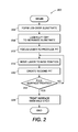
- FIG. 2 shows a flow chart describing the operations used to separate a LED from a substrate and to roughen the surface of the LED.
- FIG. 3 shows a side cross sectional view of the pits created by a roughening laser.
- FIG. 4 shows a top view of example pits created by a roughening laser.
- FIG. 5 shows a top view of example closely spaced pits created by a roughening laser.
- FIG. 6 shows using a system used to create a laser interference pattern such that regions of constructive interference forms lines that roughen a LED surface.
- FIG. 7 shows example intensity patterns in laser spots used for laser lift off and to roughen a LED surface.
- FIG. 1 shows a LED structure 100 formed over a sapphire substrate 104 .
- an intermediate template layer 108 typically made up of a nitride compound separates a n-doped region of the LED from the substrate 104 .
- typical nitride compounds include GaN, AlN, InGaN, AIInGaN, or AlGaN.
- the template layer 108 helps match the lattice structure of the n-doped cladding to the substrate lattice structure.
- substrate 104 is a sapphire substrate.
- the LED shown in FIG. 1 includes a n-doped layer 112 , a multiple quantum well active layer 116 and a p-doped cladding layer 120 all formed over template layer 108 .
- a n electrode 124 and a p electrode 128 provides current that flows into the active layer 116 to generate spontaneous emission of light.
- the active region is a AlGaN active region, the light output is in the UV range at wavelengths between 200 nm and 365 nm.
- FIG. 2 shows a flow chart 200 that describes the process of removing the sapphire substrate using a laser lift off process and roughening the laser lift off surface of the LED to improve light extraction from the LED structure in the direction 132 of FIG. 1 .
- Box 204 of FIG. 2 describes forming a LED structure similar to that shown in FIG. 1 over a sapphire substrate.
- box 208 shows use of a laser lift off process (hereinafter LLO process).
- LLO process a defocused, homogenous Laser lift off laser (LLO laser) such as an excimer laser in the desired frequency range is used.
- LLO laser Laser lift off laser
- the spot size of the laser at the laser lift off surface exceeds 1 mm 2 to enable coverage of the entire area between the substrate and the LED, however smaller spot sizes may be used if they are stitched together properly.
- LLO process a laser lift off process
- the light energy be homogenous, or spread uniformly across the laser spot area, as a non-uniform light intensity will result in decomposition region of non-uniform thickness.
- FIG. 7 illustrates the difference between a laser spot with a non-uniform light intensity and laser spot with a homogenous light intensity distribution.
- a cross-section of the light energy density of a homogenous laser spot 702 , and a non-uniform laser spot 704 are shown, with the y-axis 706 representing light intensity.
- beam uniformity is a characteristic of the laser source, however by inserting a beam homogenizer optic which is typically an array of lenslets, the spot uniformity can be improved.
- a non-uniform beam can typically be achieved by inserting a single lens and using this to focus the beam into a small spot.
- a homogenous beam is one where 80% of the spot area does not vary in intensity by +/ ⁇ 10%.
- Example laser intensity distribution in Laser spot 702 is an example of the uniform light intensity across a laser spot preferred for laser lift off.
- the LLO laser is adjusted such that sufficient power per unit area is delivered to decompose a layer of the semiconductor into nitrogen gas and an alloy of the constitutive metals. This process typically results in the vaporization of the nitrogen in the LLO absorption layer and the brief melting, but not vaporization, of the metallic elements in the LLO absorption layer.
- the LLO absorption layer is defined as the layer that absorbs most of the energy from the LLO laser.
- Typical power densities to achieve the liberation of nitrogen gas and the melting of the constitutive metals are between 600 mJ/cm 2 and 1000 mJ/cm 2 . Although power densities higher than this can be used to decompose the semiconductor, the excess energy may result in structurally damaged films.
- LLO surfaces shall be defined as surfaces that were previously attached but were separated due to a laser lift off process.
- the LLO surface of the LED is the surface of the n-doped layer 112 formerly attached to template layer 108 .
- the LLO surface of the LED will be the bottom surface of template layer 108 .
- LLO laser lift off process
- Box 212 - 220 shows a laser roughening process in which the template layer 108 is exposed to a second laser, a “roughening” laser, to create “pits” in the laser lift off (LLO) surface.
- pit is broadly defined to include any indentation in the material caused by the laser.
- the LLO surface of the LED is defined as the surface of the LED from which the substrate was removed via a laser lift off process; thus the LED laser lift off surface may be either a surface of the n-doped layer 112 or a bottom surface of the template layer 108 depending on where the substrate and the LED structure separates.
- the roughening laser delivers significantly more power per unit area than the LLO laser, usually with a non-uniform light intensity across the spot.
- the roughening laser delivers an energy density (power per unit area) in excess of 2 J/cm 2 .
- the roughening laser is focused to form a small spot size having an area less than 0.01 mm 2 to avoid creating large area pits.
- a non-uniform light intensity is preferred for roughening because a non-uniform light intensity will result in a non-uniform decomposition layer thickness, or surface roughness.
- An example non-uniform laser intensity distribution is shown in example laser spot 704 , although it should be understood that other non-uniform laser intensity distributions may also be used.
- the semiconductor absorption layer absorbs the incident roughening laser light causing a rapid temperature increase that breaks the chemical bonds of the semiconductor and decomposes it into nitrogen gas and a mixture of the liquid metals.
- the non-uniform distribution of light intensity within the spot results in variations in heating and absorption depth in the LED heterostructure. Regions of the absorption layer receiving a higher illumination density will undergo a greater temperature increase. Furthermore in such regions, the light energy will penetrate deeper and decomposition will occur deeper in the LED. These regions will not only undergo nitrogen gas vaporization, but also vaporization of the various constituent metals as well. This process can produce a curved pit shape as illustrated in FIG. 3 .
- the surface roughness produced by the roughening laser defeats losses due total internal reflection within the LED structure.
- the exact requirements necessary to defeat total internal reflection are varied, however feature sizes ranging from 100 nm to 2 microns have been show to overcome internal reflection and enhance light extraction from LEDs.
- the frequency of the laser should be selected such that the energy will be absorbed by the LLO surface of the LED.
- the laser is a frequency quadrupled Nd: YAG laser outputting light at a wavelength near 266 nm.
- Experimental results show that the thin film of Al/Ga metal that typically coats the LLO surface of the LED after a LLO procedure does not appreciably change the laser spot size (or other parameters) of the roughening laser at the LLO surface.
- the 266 nm wavelength has been show to work with a wide range of aluminum contents.
- this process works best when the ratio of Aluminum to Gallium is less than 57 Al to 43 Ga, although we have found it possible to pit the surface of an AlGaN alloy with a ratio of 7:3 Al to Ga with a 266 nm laser. Focused Excimer lasers outputting 248 nm have also been shown to work in pitting AlGaN layers with up to 70% Al content, and a 193 nm excimer laser would pit films with up to 100% Al (AlN).
- the focused laser is pulsed to create a first pit.
- each pulse of the focused pulsed second laser produces a pit or an inverted “volcano” shape in the laser lift off surface. In order to create a “rough” surface, many such pits are needed.
- relative motion between the roughening laser and the substrate moves the laser to a second position over the LLO surface of the LED. Typically the relative motion is accomplished by moving the second laser along a line or other predetermined pattern.
- the roughening laser is pulsed again to create a second pit.
- the position of the second pit is typically in such close proximity to the first pit that there is no smooth or unaffected area between the adjacent pits.
- the process is repeated, typically by moving the roughening laser along a pattern (such as a line and subsequently along an adjacent parallel line), until it is determined in box 224 that the entire LLO surface to be roughened has been sufficiently pitted or otherwise roughened.
- the LLO process along with the roughening process typically leaves behind a highly reflective gallium and aluminum metal residue over the LLO surface.
- the metal residue should be removed to reduce reflectivity and allow light from the LED active region to exit through the LLO surface.
- One method of removing the metallic residue is via a mild etch such as a hydrochloric acid (HCI) etch.
- HCI hydrochloric acid
- Box 228 shows using a HCL etch to remove the metallic residue.
- the HCL etch is typically done with a HCL concentration of 1:1 HCI:H 2 O and for a period of time less than 5 minutes.
- the HCL etch is much milder than the KOH etch traditionally used to roughen a surface, thus the HCL etch does not require protection of all the exposed contact surfaces.
- FIG. 3 shows a side cross section of a resulting pitted laser lift off surface.
- FIG. 4 shows an example top view of such a surface.
- each pit 304 , 308 typically has somewhat gently curved sides 310 that do not coincide with crystal planes.
- An approximately flat bottom 312 , 316 typically forms at the bottom of each pit 304 , 308 .
- Typical separation distances 320 between adjacent pit centers is usually between 10 to 20 microns.
- pit centers correspond to the center of a laser pulse where the light intensity is greatest, thus laser pulse spacing is typically also between 10 to 20 microns.
- Typical pit depths 324 range between 100 and 2000 nm.
- the shape of the pit is related to the non-uniformity of the light intensity within the laser spot. Controlling this non-uniformity allows control of the pit profile.
- FIG. 4 shows an example top view of the pitted LLO surface.
- Each laser pit 304 , 308 typically has a somewhat oval shape although other shapes are also possible, and likely due to variations in laser quality and optics.
- the separation distance 404 between adjacent laser pits along the short axis 412 is approximately 10 microns while the separation distance 408 along the long axis 416 is approximately 20 microns although these dimensions may vary widely depending on the desired surface roughness.
- FIG. 5 is a top view of a series of laser spots that are placed so closely together along a line 504 , that the laser spots substantially overlap.
- Each pit is typically surrounded by a “heat affected zone”, herein defined as a region in which the temperature is elevated, but the nitrogen vaporization and metal melting is incomplete or at least inhomogeneous, preventing a smooth surface from forming.
- the outer edge of the first heat affected zone 508 of AlGa metal from the first laser pit is shown at a first end of a series of such heat affected zones along line 504 .
- a second pit is formed within the outer perimeter of the first pit corresponding to the first laser spot such that the outer edge of the second heat affected zone 512 forms a ring of Al Ga metal that is almost parallel, shifted but not quite in a concentric ring adjacent to the first heat affected zone.
- the laser pulses continue along line 504 until the last laser pulse in the line is formed.
- the last pit centered at point 516 forms the last heat affected zone 520 of AlGa metal.
- Experimental results show that an AlGa surface feature forms near the center of spot 516 .
- the surface feature has a somewhat higher reflectivity than the approximate surrounding ring of AlGa metal 524 .
- FIG. 6 shows a setup to create a line pattern using a laser interference pattern.
- a laser source 604 directs laser light 608 through a beam splitter 610 .
- Mirrors 612 , 616 direct the spit beams 620 , 624 to recombine back at the LLO surface 628 , typically an AlGaN or GaN surface where the recombined beams create a laser interference pattern.
- the interference pattern includes regions of constructive interference where the roughening laser intensity is sufficient to decompose the LLO surface material.
- the interference pattern also includes regions of destructive interference where the roughening laser intensity is weak and does not pit or significantly alter the LLO surface material.
- the substrate or laser system may be rotated to create intersecting lines thereby creating a roughened surface.
- LEDs operating in the UV region of the electromagnetic spectrum may also be useful at longer wavelengths as permitted by the nitride semiconductor material system. This may include wavelengths into the visible spectrum such as violet, blue, and green light, or the wavelength spectrum extending from 365 nm to 550 nm.
- LEDs as this wavelength typically employ Ga and In rich alloys of AlGaN, InGaN, AIInN, and AlInGaN, and may include InN and GaN as well.
- the residual surface metal combinations left after the roughening process on these materials may require different etch chemistries to remove, however, HCl is know to be effective at removing Ga metal.
- substrates of SiC or GaN may be substituted for the sapphire substrate we describe.
Landscapes
- Led Devices (AREA)
- Weting (AREA)
Abstract
Description
Claims (19)
Priority Applications (1)
| Application Number | Priority Date | Filing Date | Title |
|---|---|---|---|
| US12/337,491 US7749782B1 (en) | 2008-12-17 | 2008-12-17 | Laser roughening to improve LED emissions |
Applications Claiming Priority (1)
| Application Number | Priority Date | Filing Date | Title |
|---|---|---|---|
| US12/337,491 US7749782B1 (en) | 2008-12-17 | 2008-12-17 | Laser roughening to improve LED emissions |
Publications (2)
| Publication Number | Publication Date |
|---|---|
| US20100151602A1 US20100151602A1 (en) | 2010-06-17 |
| US7749782B1 true US7749782B1 (en) | 2010-07-06 |
Family
ID=42241018
Family Applications (1)
| Application Number | Title | Priority Date | Filing Date |
|---|---|---|---|
| US12/337,491 Active 2029-01-22 US7749782B1 (en) | 2008-12-17 | 2008-12-17 | Laser roughening to improve LED emissions |
Country Status (1)
| Country | Link |
|---|---|
| US (1) | US7749782B1 (en) |
Cited By (6)
| Publication number | Priority date | Publication date | Assignee | Title |
|---|---|---|---|---|
| US20100148197A1 (en) * | 2008-12-17 | 2010-06-17 | Palo Alto Research Center Incorporated | Selective decomposition of nitride semiconductors to enhance led light extraction |
| US20110169033A1 (en) * | 2008-12-25 | 2011-07-14 | Takahiro Fukunaga | Lead, wiring member, package part, metal part provided with resin and resin-sealed semiconductor device, and methods for producing same |
| WO2013105004A1 (en) | 2012-01-10 | 2013-07-18 | Koninklijke Philips N.V. | Controlled led light output by selective area roughening |
| WO2013105015A1 (en) | 2012-01-12 | 2013-07-18 | Koninklijke Philips N.V. | Sidewall etching of led die to improve light extraction |
| US8823032B2 (en) | 2011-11-23 | 2014-09-02 | Industrial Technology Research Institute | Light-emitting diode element, method for manufacturing light guide structure thereof and equipment for forming the same |
| US11239389B2 (en) * | 2019-04-18 | 2022-02-01 | Innolux Corporation | Method for manufacturing light-emitting element and electronic device applying light-emitting element |
Families Citing this family (10)
| Publication number | Priority date | Publication date | Assignee | Title |
|---|---|---|---|---|
| US7952106B2 (en) * | 2009-04-10 | 2011-05-31 | Everlight Electronics Co., Ltd. | Light emitting diode device having uniform current distribution and method for forming the same |
| US20120241788A1 (en) * | 2010-10-29 | 2012-09-27 | Sionyx, Inc. | Textured Light Emitting Devices and Methods of Making the Same |
| TWI422068B (en) * | 2011-02-18 | 2014-01-01 | Univ Nat Cheng Kung | Roughening method and preparation method of light-emitting diode with roughened surface |
| US9064980B2 (en) * | 2011-08-25 | 2015-06-23 | Palo Alto Research Center Incorporated | Devices having removed aluminum nitride sections |
| US20130234149A1 (en) * | 2012-03-09 | 2013-09-12 | Electro Scientific Industries, Inc. | Sidewall texturing of light emitting diode structures |
| CN103022303A (en) * | 2012-12-28 | 2013-04-03 | 山东大学 | Method for implementing light emitting diode surface pattern preparation by using two-beam interference for assisting wet etching |
| GB2543090B (en) * | 2015-10-09 | 2020-02-19 | Univ Dublin City | An interference fit fastener and method of fabricating same |
| US10862002B2 (en) * | 2018-04-27 | 2020-12-08 | Facebook Technologies, Llc | LED surface modification with ultraviolet laser |
| CN111834386B (en) * | 2019-04-18 | 2025-01-14 | 群创光电股份有限公司 | Method for manufacturing light-emitting element and electronic device using light-emitting element |
| CN112967948B (en) * | 2020-08-05 | 2022-05-20 | 重庆康佳光电技术研究院有限公司 | Gallium metal removing device and gallium metal removing method |
Citations (8)
| Publication number | Priority date | Publication date | Assignee | Title |
|---|---|---|---|---|
| US6071795A (en) | 1998-01-23 | 2000-06-06 | The Regents Of The University Of California | Separation of thin films from transparent substrates by selective optical processing |
| US6562648B1 (en) | 2000-08-23 | 2003-05-13 | Xerox Corporation | Structure and method for separation and transfer of semiconductor thin films onto dissimilar substrate materials |
| US6617261B2 (en) | 2001-12-18 | 2003-09-09 | Xerox Corporation | Structure and method for fabricating GaN substrates from trench patterned GaN layers on sapphire substrates |
| US20080113463A1 (en) | 2006-11-09 | 2008-05-15 | National Central University | Method of fabricating GaN device with laser |
| US20080123711A1 (en) | 2006-09-06 | 2008-05-29 | Palo Alto Research Center Incorporated | Nitride light-emitting device |
| US20090039367A1 (en) * | 2007-07-26 | 2009-02-12 | The Regents Of The University Of California | Light emitting diodes with a p-type surface bonded to a transparent submount to increase light extraction efficiency |
| US20090090932A1 (en) | 2006-09-06 | 2009-04-09 | Palo Alto Research Incorporated | Nitride semiconductor ultraviolet leds with tunnel junctions and reflective contact |
| US7547925B2 (en) | 2005-11-14 | 2009-06-16 | Palo Alto Research Center Incorporated | Superlattice strain relief layer for semiconductor devices |
-
2008
- 2008-12-17 US US12/337,491 patent/US7749782B1/en active Active
Patent Citations (10)
| Publication number | Priority date | Publication date | Assignee | Title |
|---|---|---|---|---|
| US6071795A (en) | 1998-01-23 | 2000-06-06 | The Regents Of The University Of California | Separation of thin films from transparent substrates by selective optical processing |
| US6420242B1 (en) | 1998-01-23 | 2002-07-16 | The Regents Of The University Of California | Separation of thin films from transparent substrates by selective optical processing |
| US6562648B1 (en) | 2000-08-23 | 2003-05-13 | Xerox Corporation | Structure and method for separation and transfer of semiconductor thin films onto dissimilar substrate materials |
| US6617261B2 (en) | 2001-12-18 | 2003-09-09 | Xerox Corporation | Structure and method for fabricating GaN substrates from trench patterned GaN layers on sapphire substrates |
| US7547925B2 (en) | 2005-11-14 | 2009-06-16 | Palo Alto Research Center Incorporated | Superlattice strain relief layer for semiconductor devices |
| US20080123711A1 (en) | 2006-09-06 | 2008-05-29 | Palo Alto Research Center Incorporated | Nitride light-emitting device |
| US20080144688A1 (en) | 2006-09-06 | 2008-06-19 | Palo Alto Research Center Incorporated | Light emitting devices with an electrically active top reflector contact |
| US20090090932A1 (en) | 2006-09-06 | 2009-04-09 | Palo Alto Research Incorporated | Nitride semiconductor ultraviolet leds with tunnel junctions and reflective contact |
| US20080113463A1 (en) | 2006-11-09 | 2008-05-15 | National Central University | Method of fabricating GaN device with laser |
| US20090039367A1 (en) * | 2007-07-26 | 2009-02-12 | The Regents Of The University Of California | Light emitting diodes with a p-type surface bonded to a transparent submount to increase light extraction efficiency |
Non-Patent Citations (4)
| Title |
|---|
| Bour et al: U.S. Appl. No. 12/337,505 entitled "Selective Decomposition Of Nitride Semiconductors To Enhance LED Light Extraction" filed Dec. 17, 2008. |
| Chih-Chiang Kao, H.C. Kuo, K.F. Yeh, J.T. Chen, W.L. Peng, H.W. Huang, T.C. Lu, and S.C. Wang, "Light-Output Enhancement of Nano-Roughness GaN Laser Lift-Off Light-Emitting Diodes Formed by ICP Dry Etching," IEEE Photonics Technology Letters, 19, (11), Jun. 1, 2007, pp. 849. |
| M. K. Kelley, O. Ambacher, B. Dahlheimer, G. Groos, R. Dimitrov, H. Angerer, and M. Stutzmann, "Optical patterning of GaN films," Applied Physics Letters, 69 (12), Sep. 16, 1996, p. 1749. |
| T. Fujii, Y. Gao, R. Sharma, E. L. Hu, S. P. DenBaars, and S. Nakamura, "Increase in the extraction efficiency of GaN-based light-emitting diodes via surface roughening." Applied Physics Letters. 84, (6), Feb. 9, 2004, p. 855. |
Cited By (12)
| Publication number | Priority date | Publication date | Assignee | Title |
|---|---|---|---|---|
| US20100148197A1 (en) * | 2008-12-17 | 2010-06-17 | Palo Alto Research Center Incorporated | Selective decomposition of nitride semiconductors to enhance led light extraction |
| US20110039360A1 (en) * | 2008-12-17 | 2011-02-17 | Palo Alto Research Center Incorporated | Selective Decomposition Of Nitride Semiconductors To Enhance LED Light Extraction |
| US8124993B2 (en) * | 2008-12-17 | 2012-02-28 | Palo Alto Research Center Incorporated | Selective decomposition of nitride semiconductors to enhance LED light extraction |
| US8470619B2 (en) | 2008-12-17 | 2013-06-25 | Palo Alto Research Center Incorporated | Selective decomposition of nitride semiconductors to enhance LED light extraction |
| US20110169033A1 (en) * | 2008-12-25 | 2011-07-14 | Takahiro Fukunaga | Lead, wiring member, package part, metal part provided with resin and resin-sealed semiconductor device, and methods for producing same |
| US8946746B2 (en) * | 2008-12-25 | 2015-02-03 | Panasonic Corporation | Lead, wiring member, package part, metal part provided with resin and resin-sealed semiconductor device, and methods for producing same |
| US9960325B2 (en) | 2008-12-25 | 2018-05-01 | Panasonic Corporation | Lead, wiring member, package part, metal part provided with resin and resin-sealed semiconductor device, and methods for producing same |
| US8823032B2 (en) | 2011-11-23 | 2014-09-02 | Industrial Technology Research Institute | Light-emitting diode element, method for manufacturing light guide structure thereof and equipment for forming the same |
| WO2013105004A1 (en) | 2012-01-10 | 2013-07-18 | Koninklijke Philips N.V. | Controlled led light output by selective area roughening |
| US10074772B2 (en) | 2012-01-10 | 2018-09-11 | Lumileds Llc | Controlled LED light output by selective area roughening |
| WO2013105015A1 (en) | 2012-01-12 | 2013-07-18 | Koninklijke Philips N.V. | Sidewall etching of led die to improve light extraction |
| US11239389B2 (en) * | 2019-04-18 | 2022-02-01 | Innolux Corporation | Method for manufacturing light-emitting element and electronic device applying light-emitting element |
Also Published As
| Publication number | Publication date |
|---|---|
| US20100151602A1 (en) | 2010-06-17 |
Similar Documents
| Publication | Publication Date | Title |
|---|---|---|
| US7749782B1 (en) | Laser roughening to improve LED emissions | |
| US11820119B2 (en) | Laser lift off systems and methods that overlap irradiation zones to provide multiple pulses of laser irradiation per location at an interface between layers to be separated | |
| KR100849779B1 (en) | How to separate the material layer | |
| KR101362633B1 (en) | Laser lift-off method and laser lift-off apparatus | |
| US8163582B2 (en) | Method for fabricating a light emitting diode chip including etching by a laser beam | |
| US7419912B2 (en) | Laser patterning of light emitting devices | |
| JP5073915B2 (en) | Manufacturing method of semiconductor device | |
| US8735772B2 (en) | Method and apparatus for improved laser scribing of opto-electric devices | |
| KR101323585B1 (en) | Solid-state laser lift-off apparatus and lift-off method | |
| CN102986005B (en) | Laser peeling device | |
| JP2003168820A (en) | Peeling method, laser beam irradiation method, and device manufacturing method using these | |
| CN103348463A (en) | Method and apparatus for improved singulation of light emitting device | |
| TWI788472B (en) | Method for producing semiconductor light emitting element | |
| KR20140107121A (en) | Method of manufacturing led device, wafer substrate for manufacturing led device and apparatus for manufacturing led device | |
| JP2012015150A (en) | Laser lift-off method and laser lift-off system | |
| JP2021504933A5 (en) | ||
| US7001824B2 (en) | Gallium nitride vertical light emitting diode structure and method of separating a substrate and a thin film in the structure | |
| JP5240318B2 (en) | Laser lift-off method | |
| US11289620B2 (en) | Method of producing optoelectronic semiconductor chips and optoelectronic semiconductor chip | |
| Delmdahl et al. | Line beam laser lift-off approach for sapphire removal | |
| Wang et al. | Laser micromachining and micro-patterning with a nanosecond UV laser | |
| JP2009010427A (en) | Method for manufacturing light emitting device |
Legal Events
| Date | Code | Title | Description |
|---|---|---|---|
| AS | Assignment |
Owner name: PALO ALTO RESEARCH CENTER INCORPORATED,CALIFORNIA Free format text: ASSIGNMENT OF ASSIGNORS INTEREST;ASSIGNORS:KNOLLENBERG, CLIFFORD F, ,;BOUR, DAVID P, ,;CHUA, CHRISTOPHER L, ,;AND OTHERS;REEL/FRAME:022079/0745 Effective date: 20081216 Owner name: PALO ALTO RESEARCH CENTER INCORPORATED, CALIFORNIA Free format text: ASSIGNMENT OF ASSIGNORS INTEREST;ASSIGNORS:KNOLLENBERG, CLIFFORD F, ,;BOUR, DAVID P, ,;CHUA, CHRISTOPHER L, ,;AND OTHERS;REEL/FRAME:022079/0745 Effective date: 20081216 |
|
| FEPP | Fee payment procedure |
Free format text: PAYOR NUMBER ASSIGNED (ORIGINAL EVENT CODE: ASPN); ENTITY STATUS OF PATENT OWNER: LARGE ENTITY |
|
| STCF | Information on status: patent grant |
Free format text: PATENTED CASE |
|
| FPAY | Fee payment |
Year of fee payment: 4 |
|
| MAFP | Maintenance fee payment |
Free format text: PAYMENT OF MAINTENANCE FEE, 8TH YEAR, LARGE ENTITY (ORIGINAL EVENT CODE: M1552) Year of fee payment: 8 |
|
| MAFP | Maintenance fee payment |
Free format text: PAYMENT OF MAINTENANCE FEE, 12TH YEAR, LARGE ENTITY (ORIGINAL EVENT CODE: M1553); ENTITY STATUS OF PATENT OWNER: LARGE ENTITY Year of fee payment: 12 |
|
| AS | Assignment |
Owner name: XEROX CORPORATION, CONNECTICUT Free format text: ASSIGNMENT OF ASSIGNORS INTEREST;ASSIGNOR:PALO ALTO RESEARCH CENTER INCORPORATED;REEL/FRAME:064038/0001 Effective date: 20230416 |
|
| AS | Assignment |
Owner name: CITIBANK, N.A., AS COLLATERAL AGENT, NEW YORK Free format text: SECURITY INTEREST;ASSIGNOR:XEROX CORPORATION;REEL/FRAME:064760/0389 Effective date: 20230621 |
|
| AS | Assignment |
Owner name: XEROX CORPORATION, CONNECTICUT Free format text: CORRECTIVE ASSIGNMENT TO CORRECT THE REMOVAL OF US PATENTS 9356603, 10026651, 10626048 AND INCLUSION OF US PATENT 7167871 PREVIOUSLY RECORDED ON REEL 064038 FRAME 0001. ASSIGNOR(S) HEREBY CONFIRMS THE ASSIGNMENT;ASSIGNOR:PALO ALTO RESEARCH CENTER INCORPORATED;REEL/FRAME:064161/0001 Effective date: 20230416 |
|
| AS | Assignment |
Owner name: JEFFERIES FINANCE LLC, AS COLLATERAL AGENT, NEW YORK Free format text: SECURITY INTEREST;ASSIGNOR:XEROX CORPORATION;REEL/FRAME:065628/0019 Effective date: 20231117 |
|
| AS | Assignment |
Owner name: XEROX CORPORATION, CONNECTICUT Free format text: TERMINATION AND RELEASE OF SECURITY INTEREST IN PATENTS RECORDED AT RF 064760/0389;ASSIGNOR:CITIBANK, N.A., AS COLLATERAL AGENT;REEL/FRAME:068261/0001 Effective date: 20240206 Owner name: CITIBANK, N.A., AS COLLATERAL AGENT, NEW YORK Free format text: SECURITY INTEREST;ASSIGNOR:XEROX CORPORATION;REEL/FRAME:066741/0001 Effective date: 20240206 |
|
| AS | Assignment |
Owner name: U.S. BANK TRUST COMPANY, NATIONAL ASSOCIATION, AS COLLATERAL AGENT, CONNECTICUT Free format text: FIRST LIEN NOTES PATENT SECURITY AGREEMENT;ASSIGNOR:XEROX CORPORATION;REEL/FRAME:070824/0001 Effective date: 20250411 |
|
| AS | Assignment |
Owner name: U.S. BANK TRUST COMPANY, NATIONAL ASSOCIATION, AS COLLATERAL AGENT, CONNECTICUT Free format text: SECOND LIEN NOTES PATENT SECURITY AGREEMENT;ASSIGNOR:XEROX CORPORATION;REEL/FRAME:071785/0550 Effective date: 20250701 |