US7745302B2 - Method for making transmission electron microscope grid - Google Patents
Method for making transmission electron microscope grid Download PDFInfo
- Publication number
- US7745302B2 US7745302B2 US12/339,337 US33933708A US7745302B2 US 7745302 B2 US7745302 B2 US 7745302B2 US 33933708 A US33933708 A US 33933708A US 7745302 B2 US7745302 B2 US 7745302B2
- Authority
- US
- United States
- Prior art keywords
- carbon nanotube
- substrate
- array
- nanotube films
- making
- Prior art date
- Legal status (The legal status is an assumption and is not a legal conclusion. Google has not performed a legal analysis and makes no representation as to the accuracy of the status listed.)
- Active
Links
Images


Classifications
-
- H—ELECTRICITY
- H01—ELECTRIC ELEMENTS
- H01J—ELECTRIC DISCHARGE TUBES OR DISCHARGE LAMPS
- H01J37/00—Discharge tubes with provision for introducing objects or material to be exposed to the discharge, e.g. for the purpose of examination or processing thereof
- H01J37/02—Details
- H01J37/20—Means for supporting or positioning the object or the material; Means for adjusting diaphragms or lenses associated with the support
-
- H—ELECTRICITY
- H01—ELECTRIC ELEMENTS
- H01J—ELECTRIC DISCHARGE TUBES OR DISCHARGE LAMPS
- H01J2237/00—Discharge tubes exposing object to beam, e.g. for analysis treatment, etching, imaging
- H01J2237/20—Positioning, supporting, modifying or maintaining the physical state of objects being observed or treated
- H01J2237/2007—Holding mechanisms
-
- H—ELECTRICITY
- H01—ELECTRIC ELEMENTS
- H01J—ELECTRIC DISCHARGE TUBES OR DISCHARGE LAMPS
- H01J2237/00—Discharge tubes exposing object to beam, e.g. for analysis treatment, etching, imaging
- H01J2237/26—Electron or ion microscopes
- H01J2237/28—Scanning microscopes
- H01J2237/2802—Transmission microscopes
-
- Y—GENERAL TAGGING OF NEW TECHNOLOGICAL DEVELOPMENTS; GENERAL TAGGING OF CROSS-SECTIONAL TECHNOLOGIES SPANNING OVER SEVERAL SECTIONS OF THE IPC; TECHNICAL SUBJECTS COVERED BY FORMER USPC CROSS-REFERENCE ART COLLECTIONS [XRACs] AND DIGESTS
- Y10—TECHNICAL SUBJECTS COVERED BY FORMER USPC
- Y10S—TECHNICAL SUBJECTS COVERED BY FORMER USPC CROSS-REFERENCE ART COLLECTIONS [XRACs] AND DIGESTS
- Y10S438/00—Semiconductor device manufacturing: process
- Y10S438/96—Porous semiconductor
Definitions
- the disclosure relates to a method for making an electron microscope grid, and particularly to a method for making a transmission electron microscope grid.
- TEM Transmission electron microscopy
- the TEM technique provides high resolution imaging and material analysis of thin specimens in the range of 0.01-0.2 microns ( ⁇ m).
- a metal grid such as a copper or nickel grid covered by a porous organic membrane is provided, then evaporation is used to deposit an amorphous carbon film on the porous organic membrane.
- the amorphous carbon film can negatively impact TEM imaging.
- Carbon nanotubes have a high Young's modulus, high thermal conductivity, and high electrical conductivity, a strong absorbability, among other properties, and are considered as being potentially ideal material for making TEM grids.
- CNTs Carbon nanotubes
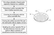
- FIG. 1 is a flow chart of a method for fabricating a TEM grid, in accordance with one embodiment.
- FIGS. 2A-2D illustrate the preparation of the TEM grid of FIG. 1 .
- FIG. 3 is a schematic view of the TEM grid formed by the method of FIG. 1 .
- FIG. 4 shows a Scanning Electron Microscope (SEM) image of the TEM grid of FIG. 3 .
- FIG. 5 shows a Transmission Electron Microscope (TEM) image of a CNT film of the TEM grid.
- TEM Transmission Electron Microscope
- FIG. 6 shows a TEM image of gold nano-particles observed by a TEM adopting the TEM grid.
- FIG. 7 is an enlarged view of FIG. 6 .
- a method for fabricating a TEM grid includes the steps of: (a) providing an array of carbon nanotubes (CNTs).
- CNTs carbon nanotubes
- a super-aligned array of CNTs is used.
- a CNT array be formed by the substeps of: (a1) providing a flat and smooth substrate; (a2) forming a catalyst layer on the substrate; (a3) annealing the substrate with the catalyst at a temperature in the approximate range from 700° C. to 900° C. in air for about 30 to 90 minutes; (a4) heating the substrate with the catalyst at a temperature in the approximate range from 500° C. to 740° C. with a protective gas therein; and (a5) supplying a carbon source gas for about 5 to 30 minutes and growing a super-aligned array of the CNTs from the substrate.
- the substrate can be a P-type silicon wafer, an N-type silicon wafer, or a silicon wafer with a film of silicon dioxide thereon.
- a 4-inch P-type silicon wafer is used as the substrate in the present embodiment.
- the catalyst can be made of iron (Fe), cobalt (Co), nickel (Ni), or an alloy thereof.
- the protective gas can be made up of at least one of nitrogen (N 2 ), ammonia (NH 3 ), and a noble gas.
- the carbon source gas can be a hydrocarbon gas, such as ethylene (C 2 H 4 ), methane (CH 4 ), acetylene (C 2 H 2 ), ethane (C 2 H 6 ), or any combination thereof.
- the array of CNTs can have a height of about 50 ⁇ m to 5 mm and includes a plurality of CNTs paralleled to each other and substantially perpendicular to the substrate.
- the array of CNTs formed under the above conditions is essentially free of impurities, such as carbonaceous or residual catalyst particles.
- the CNTs in the array are packed closely together by van Der Waals force.
- the method for fabricating the TEM grid further includes the steps of: (b) drawing a CNT film 16 from the array of CNTs.
- the first CNT film 16 can be drawn out from the CNT array by the substeps of: (b1) selecting a CNT segment having a predetermined width from the array of CNTs; and (b2) pulling a plurality CNT segments at an even/uniform speed to form the uniform CNT film 16 .
- step (b1) the CNT segments, having a predetermined width, can be selected by using an adhesive tape as a tool to contact the array.
- step (b2) the pulling direction can be substantially perpendicular to the growing direction of the array of CNTs.
- the CNT film 16 produced in such manner can be selectively formed having a predetermined width.
- the CNT film 16 includes a plurality of CNT segments.
- the CNTs in the CNT film 16 are mainly parallel to the pulling direction of the CNT film 16 .
- the width and length of the CNT film 16 depends on the size of the array of CNTs. In one embodiment, when the size of the substrate is 4 inches, the width of the CNT film 16 ranges from about 1 centimeter to about 10 centimeters. The distance between two adjacent CNTs in the CNT film 16 is less than 10 microns.
- the method for fabricating the TEM grid further includes the steps of: (c) providing a substrate 12 and a plurality of metal grids 14 mounted on the substrate 12 .
- the substrate 12 has a flat surface on which the grids 14 are mounted.
- the substrate 12 can be made of ceramic, metal and glass.
- the substrate 12 is made of ceramic.
- Each grid 14 comprises of metal and defines one or a plurality of through holes.
- Each of the through holes has a diameter ranging from about 10 microns ( ⁇ m) to about 2 millimeters (mm). The diameter of each through hole is much larger than the distance between any two adjacent CNTs in the CNT film 16 , or larger than the sizes of pores distributed in the CNT film structure if a plurality of stacked CNT films 16 is used.
- step (d) a plurality of CNT films 16 can be stacked and held together by van De Waals force to form a stable multi-layer CNT film structure. Additionally, the angle between the aligned directions of the stacked multi-layer CNT films 16 is from 0° to about 90°. In the present embodiment, the angle is 90 degrees.
- the CNT film 16 is adhesive. As such, in step (d), the first CNT film 16 can be directly adhered to a frame. The CNT films 16 are fixed on/to the frame at a determined angle to form the multi-layer CNT film structure. The metal girds 14 are covered by the multi-layer CNT film structure.
- the method for fabricating the TEM grid further includes the steps of: (e) treating the CNT film 16 with an organic solvent to increase the contact between the CNT film 16 and the metal grid 14 .
- the organic solvent is volatile and can be selected from the group consisting of ethanol, methanol, acetone, dichloroethane, chloroform, and combinations thereof.
- the CNT film 16 can be treated by applying the organic solvent to the CNT film 16 , such as: dropping the organic solvent from a dropper to soak the entire surface of the CNT film 16 or immersing the CNT film 16 into a container having an organic solvent therein.
- CNT strings After being soaked by the organic solvent, CNT strings will be formed by adjacent and parallel CNTs in the CNT film 16 , which are able to do so, bundling together, due to the surface tension of the organic solvent.
- part of the CNTs in the untreated CNT film 16 that are not adhered on the substrate will come into contact with the substrate after the organic solvent treatment due to the surface tension of the organic solvent. Then the contacting area of the CNT film 16 with the substrate 12 will increase, and thus, the CNT film 16 can be more firmly adhered to the surface of the substrate 12 .
- the mechanical strength and toughness of the CNT film 16 are increased and the coefficient of friction of the CNT films 16 is reduced. Also the size of the CNT film pores will increase. Macroscopically, the CNT film 16 will be approximately uniform.
- the CNT film structure having desired width and length can be formed by partially overlapping a plurality of CNT films 16 .
- the width and length of the CNT film structure are not constrained by the width and the length of the CNT film 16 extracted from the array of CNT.
- the size of pores in the CNT film structure is related to how many layers of CNT films 16 used, the more layers, the smaller the pores. For example, when the number of layers of CNT films 16 is four, the pore size ranges approximately from several nm to 1 ⁇ m.
- the pores can support nano-particles, nano-wires, nano-rods and so on for TEM observation analysis.
- the method for fabricating the TEM grid further includes the step of: (f) removing the CNT film 16 between the plurality of grids 14 to obtain a plurality of TEM grid.
- step (f) the CNT film covering the grids is separated from the remaining CNT film.
- a laser beam 18 is provided to remove the remaining CNT film 16 .
- the laser beam 18 can be generated by an argon ion laser or carbon dioxide laser to irradiate the CNT film 14 .
- the laser beam 18 has a power of approximately 5-30 watts. The power is 18 watts in the present embodiment.
- the CNTs of the CNT film 16 located between the grids 14 are removed by being irradiated with the focused laser beam 18 so that the CNT film 16 will be cut in a predetermined pattern.
- the laser beam 18 is focused by a lens and irradiates the surface of the CNT film 16 .
- the spot formed by the laser beam 18 irradiating the surface of the CNT film 16 has a diameter less than the distance between neighboring metal grids 14 .
- the distance between two neighboring metal grids 14 is in the range from 0.5 mm to 2 mm in the present embodiment.
- the metal grids 14 can be closely and regularly arranged on the surface of the substrate 12 .
- the metal grids 14 are configured as a matrix on the surface of the substrate 12 . It is to be understood that the laser beam 18 can irradiate the surface of the CNT film 16 perpendicularly or from an acute angle. The CNT film 16 absorbs the laser beam energy, to react with the oxygen in the air and then decompose, thus the irradiated CNTs of the CNT film 16 will be removed.
- the CNT film 16 which covers the substrate 12 and the metal grids 14 can be removed by these two methods: (1) moving to laser beam 18 to irradiate the CNT film 16 along the border of each metal grid 14 to form a separated region 144 which covers a corresponding metal grid 14 , whereby the CNT film 16 covering each grid 14 is separated from the CNT film 16 ; (2) moving the laser beam 18 to irradiate the CNT film 16 along straight lines and rows between every two metal grids 14 , to cause the separation of CNT film 16 between every two metal grids 14 .
- the moving and irradiation path of the laser beam 18 can be controlled by a computer program.
- the step of removing the CNT film 16 along the boarder of each grid 14 can be accomplished with other methods such as coating a photoresist layer on the surface of the CNT film 16 , then using physical and chemical etching to remove the CNT film 16 from around the metal grids 14 .
- a TEM grid 10 fabricated using the above-mentioned method includes a metal grid 14 and a CNT film 16 .
- the metal grid 14 having one or a plurality of through holes 142 .
- Each of the through holes 142 has an effective diameter (e.g. the largest round object that may pass through) ranging from about 10 ⁇ m to 2 mm.
- the shape of the holes can vary.
- the metal grid 14 can be made of copper, nickel or any other metal.
- the diameter of each through hole 142 is much larger than the diameters of pores distributed in the CNT film structure which may be formed a plurality of CNT films 16 are stacked.
- the effective pore size of the CNT films 16 is dependant upon the CNT films and the CNT film structure. In the present embodiment, the size of the pores in the CNT film 16 structure range approximately from 1 nm to 10 ⁇ m.
- FIG. 5 a Scanning Electron Microscope (SEM) image of the TEM grid adopting four-layer CNT films is shown.
- the angle between the aligned directions of the four-layer CNT films 16 is 90 degrees.
- Adjacent layers of the CNT films 16 are combined by van de Waals attractive force.
- the CNTs in the CNT film 16 are aligned.
- the treated CNT film includes a plurality of carbon nanotube bundles in a preferred orientation. Bundles in two adjacent layers are crossed with each other to form a microporous structure.
- a diameter of the micropores is in a range from about 1 nm to about 10 ⁇ m.
- the carbon nanotubes in the carbon nanotube array are of high-purity, uniform size, and have less defects, the TEM grid of the present embodiment interference to the morphology and structure of the samples to be observed and the high-resolution image of the nano-particles adsorbed on the carbon nanotubes is minimized.
- the small sizes of the micropores in the microporous structure of the present embodiment can be used to support nano-materials, such as nano-particles, nano-wires, nano-sticks, for the observation thereof via TEM.
- nano-materials such as nano-particles, nano-wires, nano-sticks
- the size of the nano-particles is less than 5 nm, these nano-particles can be mainly absorbed on the walls of the CNTs and can be observed.
- the dark particles are gold nano-particles to be observed according to the present embodiment.
- the gold nano-particles are absorbed on the walls of the CNTs and that is conductive to the observation of high-resolution image of gold nano-particles.
- the TEM grid of the present embodiment interference to the morphology and structure of the samples to be observed and the high-resolution image of the nano-particles absorbed on the CNTs is minimized.
- the TEM grid in the present embodiment can be formed by a CNT film drawn from an array of CNTs covered, directly, on a metal grid and the method is simple, fast and conductive to large-scale production.
- the TEM grid made by the present method has a stable property. Also, the absorption property of the CNTs is conducive to observation of high-resolution TEM image of nano-particles with a size of less than 5 nm.
Landscapes
- Chemical & Material Sciences (AREA)
- Analytical Chemistry (AREA)
- Carbon And Carbon Compounds (AREA)
Abstract
Description
Claims (15)
Applications Claiming Priority (3)
| Application Number | Priority Date | Filing Date | Title |
|---|---|---|---|
| CN200810067934 | 2008-06-20 | ||
| CN2008100679341A CN101609771B (en) | 2008-06-20 | 2008-06-20 | Fabrication method of transmission electron microscope microgrid |
| CN200810067934.1 | 2008-06-20 |
Publications (2)
| Publication Number | Publication Date |
|---|---|
| US20090317926A1 US20090317926A1 (en) | 2009-12-24 |
| US7745302B2 true US7745302B2 (en) | 2010-06-29 |
Family
ID=41431660
Family Applications (1)
| Application Number | Title | Priority Date | Filing Date |
|---|---|---|---|
| US12/339,337 Active US7745302B2 (en) | 2008-06-20 | 2008-12-19 | Method for making transmission electron microscope grid |
Country Status (2)
| Country | Link |
|---|---|
| US (1) | US7745302B2 (en) |
| CN (1) | CN101609771B (en) |
Cited By (7)
| Publication number | Priority date | Publication date | Assignee | Title |
|---|---|---|---|---|
| US20100319833A1 (en) * | 2007-03-30 | 2010-12-23 | Tsinghua University | Method for making transmission electron microscope micro-grid |
| US20110075878A1 (en) * | 2009-09-30 | 2011-03-31 | Tsinghua University | Bobbin and loudspeaker using the same cross-reference to related applications |
| US20110096952A1 (en) * | 2009-10-23 | 2011-04-28 | Tsinghua University | Diaphragm, method making the same and loudspeaker using the same |
| US20110192988A1 (en) * | 2010-02-08 | 2011-08-11 | Beijing Funate Innovation Technology Co., Ltd. | Transmission electron microscope micro-grid and method for manufacturing the same |
| US20110226960A1 (en) * | 2010-03-17 | 2011-09-22 | Tsinghua University | Carbon nanotube film composite structure, transmission electron microscope grid using the same, and method for making the same |
| US20110253300A1 (en) * | 2010-04-14 | 2011-10-20 | Beijing Funate Innovation Technology Co., Ltd. | Method for making transmission electron microscope micro-grid |
| US8436303B2 (en) * | 2007-03-30 | 2013-05-07 | Tsinghua University | Transmission electron microscope micro-grid |
Families Citing this family (28)
| Publication number | Priority date | Publication date | Assignee | Title |
|---|---|---|---|---|
| CN102148115B (en) | 2010-02-08 | 2013-03-20 | 北京富纳特创新科技有限公司 | Manufacturing method for transmission electron microscope micro-gate |
| CN102148124B (en) | 2010-02-08 | 2013-04-24 | 北京富纳特创新科技有限公司 | Micro-grid of transmission electron microscope |
| CN102194623B (en) * | 2010-03-17 | 2013-11-20 | 清华大学 | Preparation method of transmission electron microscope microgrid |
| TWI396219B (en) * | 2010-03-26 | 2013-05-11 | 鴻海精密工業股份有限公司 | Transmission electron microscopy |
| TWI407479B (en) * | 2010-04-07 | 2013-09-01 | Beijing Funate Innovation Tech | Transmission electron microscope grid |
| CN101887829B (en) | 2010-04-14 | 2013-03-13 | 北京富纳特创新科技有限公司 | Preparation method of transmission electron microscope micro-grid |
| CN101866804B (en) | 2010-04-14 | 2012-05-16 | 北京富纳特创新科技有限公司 | TEM micro grid |
| CN101866803B (en) * | 2010-04-14 | 2013-03-13 | 北京富纳特创新科技有限公司 | TEM micro grid |
| CN101866805B (en) * | 2010-04-14 | 2012-03-14 | 北京富纳特创新科技有限公司 | Preparation method of TEM micro grid |
| CN101880035A (en) | 2010-06-29 | 2010-11-10 | 清华大学 | carbon nanotube structure |
| CN102315058B (en) * | 2010-07-07 | 2013-12-11 | 清华大学 | Transmission electron microscope microgrid and preparation method thereof |
| CN102452647B (en) * | 2010-10-27 | 2013-06-19 | 北京富纳特创新科技有限公司 | Carbon nanotube film carrying structure and use method thereof |
| WO2012094634A2 (en) * | 2011-01-07 | 2012-07-12 | Dune Sciences, Inc. | Functionalized carbon membranes |
| CN102794945B (en) * | 2011-05-27 | 2014-08-20 | 清华大学 | Method for preparing graphene carbon nano tube composite membrane structure |
| CN103357960B (en) | 2012-04-03 | 2016-03-09 | 清华大学 | Micro-grid cutter sweep |
| CN103357738B (en) * | 2012-04-03 | 2015-07-01 | 清华大学 | Micro grid cutting method |
| CN103663406B (en) * | 2012-09-11 | 2015-09-02 | 北京富纳特创新科技有限公司 | The preparation method of carbon nano-tube compound film |
| WO2014107704A1 (en) * | 2013-01-07 | 2014-07-10 | William Marsh Rice University | Combined electrochemical and chemical etching processes for generation of porous silicon particulates |
| CN103257066B (en) * | 2013-05-07 | 2015-05-20 | 上海华力微电子有限公司 | Preparation method of TEM (Transmission Electron Microscope) sample |
| CN103645083B (en) * | 2013-11-22 | 2016-04-27 | 上海华力微电子有限公司 | The method that TEM sample is prepared again |
| CN104730291B (en) * | 2013-12-19 | 2017-12-29 | 中芯国际集成电路制造(上海)有限公司 | TEM sample contained network supports film and preparation method thereof, TEM sample analysis method |
| CN105185679B (en) * | 2014-06-17 | 2017-04-12 | 清华大学 | TEM (transmission electron microscope) micro-grid |
| CN104616953B (en) * | 2015-02-02 | 2017-03-08 | 武汉新芯集成电路制造有限公司 | A kind of bogey and preparation method thereof |
| EP3082148A1 (en) * | 2015-04-15 | 2016-10-19 | FEI Company | Method of manipulating a sample in an evacuated chamber of a charged particle apparatus |
| CN109142615A (en) * | 2018-08-16 | 2019-01-04 | 中国科学院金属研究所 | The device and method studied for heterogeneous catalyst same position Microstructure evolution in liquid-phase catalysis system |
| CN113192816B (en) * | 2021-04-26 | 2023-11-17 | 中国科学院物理研究所 | An electron microscope grid, its preparation method and microscope products |
| CN114689414B (en) * | 2022-04-13 | 2022-11-18 | 浙江大学 | Transmission electron microscope carrier net with special structure and preparation method thereof |
| CN115440650B (en) * | 2022-09-20 | 2025-08-01 | 中国科学院光电技术研究所 | Pin type substrate holder and preparation method thereof |
Citations (4)
| Publication number | Priority date | Publication date | Assignee | Title |
|---|---|---|---|---|
| US6930313B2 (en) * | 2002-08-12 | 2005-08-16 | Hitachi, Ltd. | Emission source having carbon nanotube, electron microscope using this emission source, and electron beam drawing device |
| US7085361B2 (en) * | 2003-12-18 | 2006-08-01 | Bellsouth Intellectual Property Corporation | Methods and systems for communication from an exterior of a location |
| US20060274889A1 (en) * | 2000-10-06 | 2006-12-07 | University Of North Carolina At Chapel Hill | Method and apparatus for controlling electron beam current |
| US20080237464A1 (en) * | 2007-03-30 | 2008-10-02 | Tsinghua University | Transmission electron microscope micro-grid and method for making the same |
Family Cites Families (1)
| Publication number | Priority date | Publication date | Assignee | Title |
|---|---|---|---|---|
| CN1206697C (en) * | 2003-02-26 | 2005-06-15 | 李巧玲 | Micro grating for transmissive electron microscope and its making process |
-
2008
- 2008-06-20 CN CN2008100679341A patent/CN101609771B/en active Active
- 2008-12-19 US US12/339,337 patent/US7745302B2/en active Active
Patent Citations (4)
| Publication number | Priority date | Publication date | Assignee | Title |
|---|---|---|---|---|
| US20060274889A1 (en) * | 2000-10-06 | 2006-12-07 | University Of North Carolina At Chapel Hill | Method and apparatus for controlling electron beam current |
| US6930313B2 (en) * | 2002-08-12 | 2005-08-16 | Hitachi, Ltd. | Emission source having carbon nanotube, electron microscope using this emission source, and electron beam drawing device |
| US7085361B2 (en) * | 2003-12-18 | 2006-08-01 | Bellsouth Intellectual Property Corporation | Methods and systems for communication from an exterior of a location |
| US20080237464A1 (en) * | 2007-03-30 | 2008-10-02 | Tsinghua University | Transmission electron microscope micro-grid and method for making the same |
Cited By (16)
| Publication number | Priority date | Publication date | Assignee | Title |
|---|---|---|---|---|
| US8436303B2 (en) * | 2007-03-30 | 2013-05-07 | Tsinghua University | Transmission electron microscope micro-grid |
| US20100319833A1 (en) * | 2007-03-30 | 2010-12-23 | Tsinghua University | Method for making transmission electron microscope micro-grid |
| US20130301868A1 (en) * | 2009-09-30 | 2013-11-14 | Hon Hai Precision Industry Co., Ltd. | Bobbin and loudspeaker using the same |
| US20110075878A1 (en) * | 2009-09-30 | 2011-03-31 | Tsinghua University | Bobbin and loudspeaker using the same cross-reference to related applications |
| US8831269B2 (en) * | 2009-09-30 | 2014-09-09 | Tsinghua University | Bobbin and loudspeaker using the same |
| US8515117B2 (en) * | 2009-09-30 | 2013-08-20 | Tsinghua University | Bobbin and loudspeaker using the same |
| US9578434B2 (en) * | 2009-10-23 | 2017-02-21 | Tsinghua University | Method for making diaphragm |
| US20130309400A1 (en) * | 2009-10-23 | 2013-11-21 | Hon Hai Precision Industry Co., Ltd. | Method for making diaphragm |
| US20110096952A1 (en) * | 2009-10-23 | 2011-04-28 | Tsinghua University | Diaphragm, method making the same and loudspeaker using the same |
| US8548188B2 (en) * | 2009-10-23 | 2013-10-01 | Tsinghua University | Diaphragm, method making the same and loudspeaker using the same |
| US8207431B2 (en) * | 2010-02-08 | 2012-06-26 | Beijing Funate Innovation Technology Co., Ltd. | Transmission electron microscope micro-grid and method for manufacturing the same |
| US20110192988A1 (en) * | 2010-02-08 | 2011-08-11 | Beijing Funate Innovation Technology Co., Ltd. | Transmission electron microscope micro-grid and method for manufacturing the same |
| US8455842B2 (en) * | 2010-03-17 | 2013-06-04 | Tsinghua University | Carbon nanotube film composite structure, transmission electron microscope grid using the same, and method for making the same |
| US20110226960A1 (en) * | 2010-03-17 | 2011-09-22 | Tsinghua University | Carbon nanotube film composite structure, transmission electron microscope grid using the same, and method for making the same |
| US8141767B2 (en) * | 2010-04-14 | 2012-03-27 | Beijing Funate Innovation Technology Co., Ltd. | Method for making transmission electron microscope micro-grid |
| US20110253300A1 (en) * | 2010-04-14 | 2011-10-20 | Beijing Funate Innovation Technology Co., Ltd. | Method for making transmission electron microscope micro-grid |
Also Published As
| Publication number | Publication date |
|---|---|
| US20090317926A1 (en) | 2009-12-24 |
| CN101609771A (en) | 2009-12-23 |
| CN101609771B (en) | 2010-12-08 |
Similar Documents
| Publication | Publication Date | Title |
|---|---|---|
| US7745302B2 (en) | Method for making transmission electron microscope grid | |
| US8288723B2 (en) | Transmission electron microscope micro-grid and method for making the same | |
| US8404070B2 (en) | Carbon nanotube film composite structure, transmission electron microscope grid using the same, and method for making the same | |
| US20110226960A1 (en) | Carbon nanotube film composite structure, transmission electron microscope grid using the same, and method for making the same | |
| US20110020563A1 (en) | Carbon nanotube film composite structure, transmission electron microscope grid using the same, and method for making the same | |
| CN101964292B (en) | Graphene sheet-carbon nanotube film composite structure and preparation method thereof | |
| US8889217B2 (en) | Method of making transparent conductive film | |
| US8207431B2 (en) | Transmission electron microscope micro-grid and method for manufacturing the same | |
| US7973295B2 (en) | Method for making transparent carbon nanotube film | |
| CN102315058B (en) | Transmission electron microscope microgrid and preparation method thereof | |
| US9398733B2 (en) | Electromagnetic shielding composite | |
| JP5622632B2 (en) | Method for manufacturing transmission electron microscope grid | |
| JP2011228284A (en) | Transmission electron microscopy grid | |
| US8148685B2 (en) | Transmission electron microscope micro-grid | |
| CN101894720B (en) | Preparation method for micro-grids of transmission electron microscope (TEM) | |
| KR20180036989A (en) | Perforated sheet of graphene material | |
| US8551392B2 (en) | Method for manufacturing transmission electron microscope micro-grid | |
| TW201103862A (en) | Transmission electron microscope grid and method for making same | |
| TWI413150B (en) | Transmission electron microscope grid and method for making same | |
| TWI411005B (en) | Method for preparing TEM micro-gate | |
| TWI407479B (en) | Transmission electron microscope grid | |
| TWI396219B (en) | Transmission electron microscopy | |
| TWI416587B (en) | Method for preparing TEM micro-gate | |
| Somers | Graphitic Surface Attachment by Single-Stranded DNA and Metal Nanoparticles | |
| TW201137929A (en) | Method for making transmission electron microscope grid |
Legal Events
| Date | Code | Title | Description |
|---|---|---|---|
| AS | Assignment |
Owner name: TSINGHUA UNIVERSITY, CHINA Free format text: ASSIGNMENT OF ASSIGNORS INTEREST;ASSIGNORS:ZHANG, LI-NA;CHEN, ZHUO;FENG, CHEN;AND OTHERS;REEL/FRAME:022007/0791 Effective date: 20081202 Owner name: HON HAI PRECISION INDUSTRY CO., LTD., TAIWAN Free format text: ASSIGNMENT OF ASSIGNORS INTEREST;ASSIGNORS:ZHANG, LI-NA;CHEN, ZHUO;FENG, CHEN;AND OTHERS;REEL/FRAME:022007/0791 Effective date: 20081202 Owner name: TSINGHUA UNIVERSITY,CHINA Free format text: ASSIGNMENT OF ASSIGNORS INTEREST;ASSIGNORS:ZHANG, LI-NA;CHEN, ZHUO;FENG, CHEN;AND OTHERS;REEL/FRAME:022007/0791 Effective date: 20081202 Owner name: HON HAI PRECISION INDUSTRY CO., LTD.,TAIWAN Free format text: ASSIGNMENT OF ASSIGNORS INTEREST;ASSIGNORS:ZHANG, LI-NA;CHEN, ZHUO;FENG, CHEN;AND OTHERS;REEL/FRAME:022007/0791 Effective date: 20081202 |
|
| STCF | Information on status: patent grant |
Free format text: PATENTED CASE |
|
| FPAY | Fee payment |
Year of fee payment: 4 |
|
| MAFP | Maintenance fee payment |
Free format text: PAYMENT OF MAINTENANCE FEE, 8TH YEAR, LARGE ENTITY (ORIGINAL EVENT CODE: M1552) Year of fee payment: 8 |
|
| MAFP | Maintenance fee payment |
Free format text: PAYMENT OF MAINTENANCE FEE, 12TH YEAR, LARGE ENTITY (ORIGINAL EVENT CODE: M1553); ENTITY STATUS OF PATENT OWNER: LARGE ENTITY Year of fee payment: 12 |