US7741902B2 - Circuit and method for generating a PWM control signal for a class-D amplifier - Google Patents
Circuit and method for generating a PWM control signal for a class-D amplifier Download PDFInfo
- Publication number
- US7741902B2 US7741902B2 US12/285,710 US28571008A US7741902B2 US 7741902 B2 US7741902 B2 US 7741902B2 US 28571008 A US28571008 A US 28571008A US 7741902 B2 US7741902 B2 US 7741902B2
- Authority
- US
- United States
- Prior art keywords
- signal
- polarity
- pwm
- pulse
- input signal
- Prior art date
- Legal status (The legal status is an assumption and is not a legal conclusion. Google has not performed a legal analysis and makes no representation as to the accuracy of the status listed.)
- Expired - Fee Related, expires
Links
Images


Classifications
-
- H—ELECTRICITY
- H03—ELECTRONIC CIRCUITRY
- H03F—AMPLIFIERS
- H03F3/00—Amplifiers with only discharge tubes or only semiconductor devices as amplifying elements
- H03F3/20—Power amplifiers, e.g. Class B amplifiers, Class C amplifiers
- H03F3/21—Power amplifiers, e.g. Class B amplifiers, Class C amplifiers with semiconductor devices only
- H03F3/217—Class D power amplifiers; Switching amplifiers
Definitions
- the present invention is related generally to a class-D amplifier and, more particularly, to a single-end input class-D amplifier.
- class-D amplifiers are two to five times more efficient than class-AB amplifiers and have benefits because of the efficiency, for example, requiring smaller power supplies, eliminating heat sinks and thereby significantly reducing overall system cost, size and weight.
- the class-D amplifiers work by converting an analog or digital input signal into a two-level output signal using a high-frequency modulation process.
- This two-level signal is then fed to a power stage to switch power switches in a full or half H-bridge, which in turn feeds a passive output filter connected to a speaker.
- These power switches have very low switching loss, so that the amplifier has better efficiency.
- Most class-D amplifier systems employ a pulse width modulation (PWM) scheme, where the value of the input signal at a moment in time is represented by a fixed-voltage variable-width output pulse.
- PWM pulse width modulation
- a typical audio PWM amplifier works at a switching frequency of between 100 KHz and 500 KHz. Higher switching frequencies can reduce distortion but also result in lower efficiency due to the extra transitions in the output waveform.
- the class-D amplifiers have electromagnetic interference (EMI) problem, as do the majority of switching power management devices, since they are derived from switching power supply configuration.
- EMI electromagnetic interference
- a conventional class-D amplifier in bridge-tied-load (BTL) configuration always generates two PWM signals Out+ and Out ⁇ with 180 degrees out of phase at a pair of differential outputs, and produces the differential output (Out+) ⁇ (Out ⁇ ) which has an amplitude (2Vdd) twice as large as that of the PWM signal Out+ or Out ⁇ .
- This large amplitude results in large ripple of the load current and therefore, there is always need for an external filter to remove the high frequency switching carrier.
- This filter typically includes at least two high current inductors and three capacitors which are expensive and consume undesirable amounts of space.
- the LC filter can also ease the EMI problem since the 180 degrees out of phases PWM signals Out+ and Out ⁇ generate large EMI interference. For this reason, filterless class-D amplifiers are proposed, for example by U.S. Pat. Nos. 6,614,297, 6,847,257 and 6,970,123, which eliminate the output filter while reducing the EMI interference.
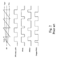
- FIG. 2 is a timing diagram to illustrate the operation of a general differential input class-D amplifier, in which two differential input signals Vin+ and Vin ⁇ are compared with a sawtooth carrier Vref, respectively, to generate two PWM signals PWM+ and PWM ⁇ whose subtraction is the output PWM signal to drive the power stage of the class-D amplifier.
- This output PWM signal has the same amplitude as those of the PWM signals PWM+ and PWM ⁇ , and thus the load current will have smaller ripple.
- the input information and the output power are designed in the difference of the signals PWM+ and PWM ⁇ . It is obvious that the pulse difference by the signals PWM+ or PWM ⁇ compared to 50% duty cycle is half of the output PWM signal, as shown in FIG. 2 . In other words, the output PWM is symmetric to the 50% duty cycle.
- the output power of a single-end input class-D amplifier would be a quarter times less than that of which uses fully differential signals as inputs under a same gain. Conventionally, the single-end input signal is always processed by a gain stage which turns the single-end input signal into a fully differential input signal.
- the subsequent ternary or quaternary PWM control signals would need to be generated by using the fully differential input signal, or under a similar idea, using two mutually 180 degrees out of phase reference waveforms of sawtooth or triangle to generate the ternary or quaternary PWM control signals.
- a new modulation scheme for class-D amplifiers is proposed under the concept illustrated in FIG. 2 , which can keep the output power as large as that by using differential input signals in prior arts although the input signal is single-end and the entire signal processing path is kept single-ended.
- an object of the present invention is to provide a circuit and method for generating a PWM control signal for a class-D amplifier.
- the input signal of a class-D amplifier is compared with a carrier signal to generate a basic PWM signal, the basic PWM signal is then sent to a pulse processing unit, and by comparing with a basic periodic signal, half-width of the output PWM signal is extracted. Then the half-width PWM pulse signal is used to generate a complete pulse whose width equals to the output PWM signal in the pulse processing unit.
- a hysteresis comparator is used to generate the basic PWM signal.
- the class-D amplifier can provide an output power as large as that by using differential input signals.
- FIG. 1 is a timing diagram to show the PWM signals of conventional class-D amplifiers
- FIG. 2 is a timing diagram to show the operation of general differential input class-D amplifiers
- FIG. 3 is a block diagram of a first embodiment according to the present invention.
- FIG. 4 is an embodiment for the pulse processing unit shown in FIG. 3 ;
- FIG. 5 is a timing diagram to show the operation of the circuit of FIG. 3 ;
- FIG. 6 is a block diagram of a second embodiment according to the present invention.
- FIG. 7 is an embodiment for the pulse processing unit shown in FIG. 6 ;
- FIG. 8 is a timing diagram to show the operation of the circuit of FIG. 6 .
- FIG. 3 is a block diagram of a first embodiment according to the present invention.
- This single-end input class-D amplifier has an input Vin to receive an input signal.
- a single-end input signal Vin When a single-end input signal Vin is detected, its polarity is to be identified first. This is done by a polarity identifying circuit 10 in a pre-processing unit.
- the polarity identifying circuit 10 may include a comparator to compare the single-end input signal Vin with a direct current (DC) voltage, for example 0 volt.
- the pre-processing unit further includes an inverter 12 and a bypass circuit 14 , both coupled to the polarity identifying circuit 10 .
- the input signal Vin would be inverted by the inverter 12 if it is positive and if it is negative, it would be bypassed to combine with the output of the inverter 12 . Therefore, the single-end input signal Vin is pre-processed by the pre-processing unit into a negative single-end input signal for a hysteresis comparator 16 to compare with a carrier signal Vref to generate a basic PWM signal.
- the carrier signal Vref may have a sawtooth or ramp waveform.
- a pulse processing unit 18 extracts half-width of the output PWM signal by comparing the basic PWM signal with a basic periodic signal, for example 50% duty cycle, and generates a complete pulse whose width equals to the output PWM signal.
- PWM control signals Ctrl_ 1 and Ctrl_ 2 are produced for a gate driver and H-bridge output power stage 20 .
- the PWM control signals Ctrl_ 1 and Ctrl_ 2 have the same pulse width and the same phase as those of the output PWM signal shown in FIG. 2 .
- FIG. 4 is an embodiment for the pulse processing unit 18 , which is now described with reference to the timing diagram shown in FIG. 5 .
- the basic periodic signal for example a clock, has a 50% duty cycle, and is subtracted from the basic PWM signal by a subtractor 182 to generate a half-width PWM signal as the waveform PWM ⁇ (50% duty cycle) shown in FIG. 5 .
- a pulse copy unit 184 copies the pulse of the half-width PWM signal to produce a complete pulse as shown by the waveform Copy of FIG. 5 .
- switches 186 and 188 are switched according to the polarity of the single-end input signal Vin to determine the output of the pulse processing unit 18 .
- the switch 186 is closed and the switch 188 is open, so that the PWM control signal Ctrl_ 1 is equal to the output PWM signal Copy and the PWM control signal Ctrl_ 2 is 0.
- the switch 186 is open and the switch 188 is closed, so that the PWM control signal Ctrl_ 1 is 0 and the PWM control signal Ctrl_ 2 is equal to the output PWM signal Copy.
- the voltage applied to the load is the difference between the PWM control signals Ctrl_ 1 and Ctrl_ 2 .
- FIG. 6 is a second embodiment according to the present invention, which has a hysteresis comparator 30 to compare the single-end input signal Vin with a carrier signal Vref, for example a sawtooth wave, so as to generate a basic PWM signal, and a pulse processing unit 32 to subtract a 50% duty cycle from the basic PWM signal to extract half width of the output PWM signal and to produce a complete pulse from the half width PWM signal. Subsequently, two PWM control signals Ctrl_ 1 and Ctrl_ 2 are produced for a gate driver and H-bridge output power stage 34 .
- FIG. 7 is an embodiment for the pulse processing unit 32 of FIG. 6
- FIG. 8 is a timing diagram to show the operation of this circuit.
- the single-end input signal Vin is not pre-processed.
- the resultant half width PWM signal is the same as that shown in the embodiment of FIG. 3 , and the waveform after being copied has the same pulse width and the same phase as those of the output PWM shown in FIG. 2 .
- the resultant half width driving signal after being copied has a different phase than that of the output PWM shown in FIG. 2 .
- a delay circuit 326 delays the after-copied half width driving signal by N clocks, so that the final output signal to the gate driver and H-bridge output power stage 34 has the correct phase. The number of delay cycles N is determined according to the designer's requirement, provided the output signal is correct in timing.
Landscapes
- Engineering & Computer Science (AREA)
- Power Engineering (AREA)
- Amplifiers (AREA)
Abstract
Description
Claims (13)
Applications Claiming Priority (3)
| Application Number | Priority Date | Filing Date | Title |
|---|---|---|---|
| TW097100382 | 2008-01-04 | ||
| TW97100382A | 2008-01-04 | ||
| TW097100382A TWI350051B (en) | 2008-01-04 | 2008-01-04 | Circuit and method for generating a pwm control signal for a class-d amplifier |
Publications (2)
| Publication Number | Publication Date |
|---|---|
| US20090174478A1 US20090174478A1 (en) | 2009-07-09 |
| US7741902B2 true US7741902B2 (en) | 2010-06-22 |
Family
ID=40844099
Family Applications (1)
| Application Number | Title | Priority Date | Filing Date |
|---|---|---|---|
| US12/285,710 Expired - Fee Related US7741902B2 (en) | 2008-01-04 | 2008-10-14 | Circuit and method for generating a PWM control signal for a class-D amplifier |
Country Status (2)
| Country | Link |
|---|---|
| US (1) | US7741902B2 (en) |
| TW (1) | TWI350051B (en) |
Cited By (2)
| Publication number | Priority date | Publication date | Assignee | Title |
|---|---|---|---|---|
| US20100253427A1 (en) * | 2009-04-03 | 2010-10-07 | Amazing Microelectronic Corp. | Class-d amplifier |
| US20120218801A1 (en) * | 2011-02-28 | 2012-08-30 | Kabushiki Kaisha Yaskawa Denki | Current-source power converting apparatus |
Families Citing this family (1)
| Publication number | Priority date | Publication date | Assignee | Title |
|---|---|---|---|---|
| TWI584579B (en) * | 2015-04-24 | 2017-05-21 | 晶豪科技股份有限公司 | Modulation selecting circuit of audio amplifier and method thereof |
Citations (4)
| Publication number | Priority date | Publication date | Assignee | Title |
|---|---|---|---|---|
| US6763114B1 (en) * | 1997-07-23 | 2004-07-13 | Microsemi Corporation | Multiple channel class D audio amplifier |
| US7183840B2 (en) * | 2003-10-17 | 2007-02-27 | Yamaha Corporation | Class-D amplifier |
| US7385444B2 (en) * | 2004-05-06 | 2008-06-10 | Nec Electronics Corporation | Class D amplifier |
| US20080284508A1 (en) * | 2007-05-15 | 2008-11-20 | Walker Brett C | Output circuits with class d amplifier |
-
2008
- 2008-01-04 TW TW097100382A patent/TWI350051B/en not_active IP Right Cessation
- 2008-10-14 US US12/285,710 patent/US7741902B2/en not_active Expired - Fee Related
Patent Citations (4)
| Publication number | Priority date | Publication date | Assignee | Title |
|---|---|---|---|---|
| US6763114B1 (en) * | 1997-07-23 | 2004-07-13 | Microsemi Corporation | Multiple channel class D audio amplifier |
| US7183840B2 (en) * | 2003-10-17 | 2007-02-27 | Yamaha Corporation | Class-D amplifier |
| US7385444B2 (en) * | 2004-05-06 | 2008-06-10 | Nec Electronics Corporation | Class D amplifier |
| US20080284508A1 (en) * | 2007-05-15 | 2008-11-20 | Walker Brett C | Output circuits with class d amplifier |
Cited By (4)
| Publication number | Priority date | Publication date | Assignee | Title |
|---|---|---|---|---|
| US20100253427A1 (en) * | 2009-04-03 | 2010-10-07 | Amazing Microelectronic Corp. | Class-d amplifier |
| US7855597B2 (en) * | 2009-04-03 | 2010-12-21 | Amazing Microelectronic Corp. | Class-D amplifier |
| US20120218801A1 (en) * | 2011-02-28 | 2012-08-30 | Kabushiki Kaisha Yaskawa Denki | Current-source power converting apparatus |
| US8947897B2 (en) * | 2011-02-28 | 2015-02-03 | Kabushiki Kaisha Yaskawa Denki | Current-source power converting apparatus |
Also Published As
| Publication number | Publication date |
|---|---|
| TWI350051B (en) | 2011-10-01 |
| US20090174478A1 (en) | 2009-07-09 |
| TW200931794A (en) | 2009-07-16 |
Similar Documents
| Publication | Publication Date | Title |
|---|---|---|
| US6614297B2 (en) | Modulation scheme for filterless switching amplifiers with reduced EMI | |
| US7468631B1 (en) | Class D amplifier | |
| US6812785B2 (en) | Digital power amplifier and digital/analog converter | |
| US7298209B1 (en) | Class D amplifier | |
| US20070146069A1 (en) | Filterless class D power amplifier | |
| US20090302943A1 (en) | Class d amplifier | |
| US20150063593A1 (en) | Noise and Cross-Talk Attenuation in an Audio System by Offsetting Outputs in Phase | |
| EP1201026A1 (en) | Break-before-make distortion compensation for a digital amplifier | |
| US20120049930A1 (en) | Apparatus and Method for Switching Audio Amplification | |
| US20170250654A1 (en) | Dynamic dead time management | |
| US7741902B2 (en) | Circuit and method for generating a PWM control signal for a class-D amplifier | |
| US9866187B2 (en) | High efficiency class D amplifier with reduced generation of EMI | |
| US8816763B2 (en) | Integrator input error correction circuit and circuit method | |
| CN106100305B (en) | DC maladjustment removing method in COT ripple compensation circuits | |
| US9847706B2 (en) | Systems and methods for reducing voltage ringing in a power converter | |
| US7173483B2 (en) | Low-distortion tri-state switching amplifier | |
| Lin et al. | Enhanced design of filterless class-D audio amplifier | |
| US11837999B2 (en) | Audio amplifier having idle mode | |
| CN101527548A (en) | Circuit and method for generating PWM control signal by D-class amplifier | |
| US7388431B2 (en) | Switching amplifier and control method thereof | |
| CN202535324U (en) | Switch circuit | |
| US7573328B2 (en) | Power amplifier | |
| KR20020034677A (en) | High-Efficiency Switching Amplifier | |
| EP3091659B1 (en) | High efficiency class d amplifier with reduced generation of emi | |
| US20070216478A1 (en) | Systems and Methods for Maintaining Minimum Pulse Width During Shutdown |
Legal Events
| Date | Code | Title | Description |
|---|---|---|---|
| AS | Assignment |
Owner name: RICHTEK TECHNOLOGY CORP., TAIWAN Free format text: ASSIGNMENT OF ASSIGNORS INTEREST;ASSIGNORS:GUO, JWIN-YEN;SUN, SHAO-MING;REEL/FRAME:021739/0552 Effective date: 20080925 Owner name: RICHTEK TECHNOLOGY CORP.,TAIWAN Free format text: ASSIGNMENT OF ASSIGNORS INTEREST;ASSIGNORS:GUO, JWIN-YEN;SUN, SHAO-MING;REEL/FRAME:021739/0552 Effective date: 20080925 |
|
| FEPP | Fee payment procedure |
Free format text: PAYOR NUMBER ASSIGNED (ORIGINAL EVENT CODE: ASPN); ENTITY STATUS OF PATENT OWNER: LARGE ENTITY Free format text: PAT HOLDER NO LONGER CLAIMS SMALL ENTITY STATUS, ENTITY STATUS SET TO UNDISCOUNTED (ORIGINAL EVENT CODE: STOL); ENTITY STATUS OF PATENT OWNER: LARGE ENTITY |
|
| FPAY | Fee payment |
Year of fee payment: 4 |
|
| FEPP | Fee payment procedure |
Free format text: MAINTENANCE FEE REMINDER MAILED (ORIGINAL EVENT CODE: REM.) |
|
| LAPS | Lapse for failure to pay maintenance fees |
Free format text: PATENT EXPIRED FOR FAILURE TO PAY MAINTENANCE FEES (ORIGINAL EVENT CODE: EXP.) |
|
| STCH | Information on status: patent discontinuation |
Free format text: PATENT EXPIRED DUE TO NONPAYMENT OF MAINTENANCE FEES UNDER 37 CFR 1.362 |
|
| FP | Lapsed due to failure to pay maintenance fee |
Effective date: 20180622 |