US7725783B2 - Method and apparatus for repeatable drive strength assessments of high speed memory DIMMs - Google Patents
Method and apparatus for repeatable drive strength assessments of high speed memory DIMMs Download PDFInfo
- Publication number
- US7725783B2 US7725783B2 US11/780,505 US78050507A US7725783B2 US 7725783 B2 US7725783 B2 US 7725783B2 US 78050507 A US78050507 A US 78050507A US 7725783 B2 US7725783 B2 US 7725783B2
- Authority
- US
- United States
- Prior art keywords
- data
- memory
- radiated
- memory device
- dimm
- Prior art date
- Legal status (The legal status is an assumption and is not a legal conclusion. Google has not performed a legal analysis and makes no representation as to the accuracy of the status listed.)
- Active, expires
Links
- 238000000034 method Methods 0.000 title claims description 20
- 239000000872 buffer Substances 0.000 claims description 14
- 238000012360 testing method Methods 0.000 claims description 13
- 230000009977 dual effect Effects 0.000 claims description 3
- 238000001228 spectrum Methods 0.000 claims description 3
- 230000005855 radiation Effects 0.000 claims description 2
- 238000013102 re-test Methods 0.000 claims 2
- 208000032767 Device breakage Diseases 0.000 claims 1
- 230000006870 function Effects 0.000 abstract description 3
- 239000000523 sample Substances 0.000 description 4
- 238000005259 measurement Methods 0.000 description 2
- 238000012986 modification Methods 0.000 description 2
- 230000004048 modification Effects 0.000 description 2
- 238000013459 approach Methods 0.000 description 1
- 230000002238 attenuated effect Effects 0.000 description 1
- 230000002457 bidirectional effect Effects 0.000 description 1
- 230000005540 biological transmission Effects 0.000 description 1
- 125000004122 cyclic group Chemical group 0.000 description 1
- 230000000694 effects Effects 0.000 description 1
- 238000012423 maintenance Methods 0.000 description 1
- 238000004806 packaging method and process Methods 0.000 description 1
- 230000003252 repetitive effect Effects 0.000 description 1
- 230000003595 spectral effect Effects 0.000 description 1
Images


Classifications
-
- G—PHYSICS
- G01—MEASURING; TESTING
- G01R—MEASURING ELECTRIC VARIABLES; MEASURING MAGNETIC VARIABLES
- G01R31/00—Arrangements for testing electric properties; Arrangements for locating electric faults; Arrangements for electrical testing characterised by what is being tested not provided for elsewhere
- G01R31/28—Testing of electronic circuits, e.g. by signal tracer
- G01R31/2801—Testing of printed circuits, backplanes, motherboards, hybrid circuits or carriers for multichip packages [MCP]
- G01R31/281—Specific types of tests or tests for a specific type of fault, e.g. thermal mapping, shorts testing
- G01R31/2815—Functional tests, e.g. boundary scans, using the normal I/O contacts
-
- G—PHYSICS
- G11—INFORMATION STORAGE
- G11C—STATIC STORES
- G11C29/00—Checking stores for correct operation ; Subsequent repair; Testing stores during standby or offline operation
- G11C29/02—Detection or location of defective auxiliary circuits, e.g. defective refresh counters
-
- G—PHYSICS
- G11—INFORMATION STORAGE
- G11C—STATIC STORES
- G11C29/00—Checking stores for correct operation ; Subsequent repair; Testing stores during standby or offline operation
- G11C29/02—Detection or location of defective auxiliary circuits, e.g. defective refresh counters
- G11C29/022—Detection or location of defective auxiliary circuits, e.g. defective refresh counters in I/O circuitry
-
- G—PHYSICS
- G11—INFORMATION STORAGE
- G11C—STATIC STORES
- G11C29/00—Checking stores for correct operation ; Subsequent repair; Testing stores during standby or offline operation
- G11C29/56—External testing equipment for static stores, e.g. automatic test equipment [ATE]; Interfaces therefor
-
- G—PHYSICS
- G01—MEASURING; TESTING
- G01R—MEASURING ELECTRIC VARIABLES; MEASURING MAGNETIC VARIABLES
- G01R31/00—Arrangements for testing electric properties; Arrangements for locating electric faults; Arrangements for electrical testing characterised by what is being tested not provided for elsewhere
- G01R31/28—Testing of electronic circuits, e.g. by signal tracer
- G01R31/302—Contactless testing
- G01R31/304—Contactless testing of printed or hybrid circuits
-
- G—PHYSICS
- G11—INFORMATION STORAGE
- G11C—STATIC STORES
- G11C29/00—Checking stores for correct operation ; Subsequent repair; Testing stores during standby or offline operation
- G11C29/56—External testing equipment for static stores, e.g. automatic test equipment [ATE]; Interfaces therefor
- G11C2029/5602—Interface to device under test
Definitions
- the present invention relates generally to high speed DIMMs and, more specifically, to an apparatus for repeatable drive strength assessments of high speed memory devices, such as DIMMs.
- a DIMM or a Dual In-line Memory Module
- the DIMM is a rectangular low-profile circuit board that has electrical contact points arranged on both sides along one long edge. The contact points form electrical connections to the main board's memory bus when the DIMM is inserted into a DIMM memory socket.
- a memory controller is a chip on a computer's motherboard or CPU die which manages the flow of data going to and from the memory.
- the disadvantage in using this kind of approach is that the trace itself produces unwanted stub loading into the probe and signal under test.
- Stub loading on the main bus can be caused by excessively long stubs and/or stubs terminated in low impedances and can load down the main bus and result in transmission line reflections, and therefore waveform distortions.
- This can have the effect of increasing the bit error rate for terminals receiving data on the bus, or in extreme circumstances, cause terminals to stop receiving completely.
- Another disadvantage is the uncertainty in being able to repeat the measurement consistently.
- a ball grid array (BGA) is a type of surface-mount packaging used for integrated circuits.)
- BGA ball grid array
- Use of sophisticated probe stations is one way to over come this limitation, but probe stations that provide this kind of measurement capability are expensive and cost 100s of thousands of dollars.
- test jig is an adapter for connecting electronic devices to a service and maintenance system for testing, debugging and firmware update purposes.
- the present invention is an apparatus for repeatable drive strength assessments of high speed memory DIMMs.
- the present invention assesses memory (DIMM) strength by calculating frequency content of a radiated field which is collected by an apparatus, such as a dipole antenna. Radiated field is created by accelerated charge, which is a function of the slew rate or DIMM strength. Radiated power is directly proportional to the frequency at which bits are driven.
- DIMM strength content is isolated from other functional DIMM issues, such as tRCD latency, refresh cycles, addressing mode, etc.
- tRCD latency RAS to CAS Delay
- tRCD latency is the number of clock cycles needed between a row address strobe (RAS) and a column address strobe (CAS).
- the illustrative aspects of the present invention are designed to solve one or more of the problems herein described and/or one or more other problems not discussed.
- FIG. 1 depicts the system of the present invention.
- FIG. 2 represents the method of the present invention.
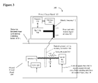
- FIG. 3 represents the system of the present invention having a dampening resistor.
- the present invention provides an apparatus for repeatable drive strength assessments of high speed memory units, such as DIMMs.
- FIG. 1 depicts the Memory System Configuration 100 of the present invention.
- a DIMM 122 (a DIMM, or dual in-line memory module, comprises a series of random access memory integrated circuits. These modules are mounted on a printed circuit board and designed for use in personal computers) communicates via Data Bus 113 with MCH 112 .
- MCH or memory controller hub, is traditionally one of the two chips in the core logic chipset on a PC motherboard, the other being the southbridge.
- the basis of the present invention is to assess DIMM strength by calculating frequency content of a radiated field. Radiated field is created by accelerated charge, which is a function of the slew rate or DIMM strength. Radiated power is directly proportional to the frequency at which bits are driven. By separating the radiated field from the near field or stored field, the DIMM strength content is isolated from other functional DIMM issues, such as TRCD latency, refresh cycles, addressing mode, etc.
- the apparatus of the preferred embodiment has two printed circuit boards, Printed Circuit Board 102 and Printed Circuit Board 104 .
- One board (Printed Circuit Board 102 ) is configured to radiate utilizing Riser with Dipole Antenna 117 from operational amplifier (Op-Amp 106 ) for amplifying the data received from Printed Circuit Board 104 .
- An Op-Amp is a DC-coupled high-gain electronic voltage amplifier with differential inputs and, usually, a single output. In its ordinary usage, the output of the op-amp is controlled by negative feedback which, because of the amplifier's high gain, almost completely determines the output voltage for any given input.
- a dipole antenna is an antenna with a center-fed driven element for transmitting or receiving radio frequency energy.
- the Dipole Antenna 117 receives data from the other (Printed Circuit Board 104 ) which transmits data from Radiating Board 108 based on the concept of reciprocity and the Op-Amp 106 amplifies the data that has been transmitted by Radiating Board 108 and the data is decoded by Decoder 110 . The data is then passed to Analyzer 114 which analyzes the data received by the Di-Pole Antenna 117 to determine the strength of the tested DIMMs (such as DIMM 122 ). On the Radiating Board 108 , is a memory controller. The memory controller exercises the DIMM during testing.
- the memory controller exercises the DIMM (such as DIMM 122 ) in read mode, so only the DIMM is driving, and in burst mode, so that an alternating current is created.
- the test results are radiated by Radiating Board 108 and received by Di-Pole Antenna 117 , amplified by Op-Amp 106 and decoded by Decoder 110 .
- Only the memory data lines are radiated in that the control signals are routed around Radiating Board 108 on Control Signal Bus 116 .
- the memory data traces (Data Bus 113 ) can be routed across open slots in the shield layer that are half a wavelength (lambda ⁇ ) long.
- Each memory controller output buffer is over damped with a series resistor which can be seen in FIG. 3 .
- the objective of the present invention is to not confuse the switching strength of the memory DIMM's output buffer with memory controller's output buffer.
- the two output buffers share the same data bus trace 113 .
- One bidirectional buffer is inside the memory controller (Memory Controller Hub 112 .
- the other is inside the memory DIMM 122 .
- the memory controller's output buffer switching strength is attenuated with an external series resistor that is located in close proximity to the memory controller. This is shown in FIG. 3 as series resistor 310 .
- the combined memory controller's output buffer and series resistor 310 act as one slow degraded driver.
- the memory device output buffer is not influenced by the series resistor and operates full strength and at maximum slew rate.
- the present invention allows the system to generate a continuous flow of data out of the memory device and onto the memory data traces (Data Bus 113 ).
- the memory controller stores, in the memory DIMM, the data pattern with the highest repetitive pattern and sets up the read operation.
- the test begins with the memory controller requesting memory data with read commands.
- the read commands are transferred from the memory controller to the memory device.
- the read commands configure the memory device to output memory data patterns that are stored in memory.
- the memory control stops transmitting and converts to receive mode.
- the memory DIMM ( 122 ) takes over the data bus, responds with its output driver switching at maximum frequency and exports the requested data pattern as a continuous stream of bits in burst mode.
- Memory DIMMs output buffer produces alternating cyclic patterns on the data trace 113 . Thus, spectral frequency associated with the radiation pattern detected is predominately produced by the memory DIMM's output buffer.
- the board is configured so the DIMM's data outs are fast switching buffers.
- a like card 102 has an electric antenna whose half wavelength (lambda ⁇ ) matches the DIMM burst mode frequency.
- the card is positioned like a riser card next to and into the radiating card.
- the signal radiated is received and amplified with the Op-Amp 106 .
- the received signal is translated into a frequency spectrum display. From the frequency spectrum display, the fundamental frequency magnitude is compared to a reference magnitude. By inspecting the fundamental frequency magnitude against the reference magnitude, the drive strength of the high speed memory device, such as DIMM 122 , may be assessed.
- FIG. 2 depicts the Method 200 of the present invention. It starts at Step 202 and continues to Step 204 where data is passed from the memory (DIMM 122 in the preferred embodiment) to a memory control hub (MCH 112 in the preferred embodiment) through a radiating board (Radiating Board 108 ).
- the data is radiated from Radiating Board 108 and is received by Di-Pole Antenna 117 .
- the Radiating Board 108 further has a Memory Controller which exercises the memory (DIMM 122 ) in read mode, so only the DIMM is driving, and in burst mode, so that an alternating current is created. This allows Analyzer 114 to analyze the data received to determine memory (DIMM in this case) strength.
- the received signals are amplified by Op-Amp 106 .
- the received signals are generally of low power level so that they need to be amplified.
- the received signals are decoded by the Decoder 110 and, at Step 212 , the decoded signals are analyzed by Analyzer 114 .
- the Analyzer 212 determines whether the DIMM strength meets the threshold and, if so, the data is recorded at Step 216 and process ends at Step 218 .
- Step 215 it is determined how many times the test has been repeated (tests may need to be repeated in the case there was a mis-measure or other misfires) and if the test repeat has not met the threshold, the test is repeated and goes to Step 204 . If the test repeat number has been reached, the process ends at 218 .
- FIG. 3 depicts the System 300 of the present invention illustrating the dampening resistor 310 .
Landscapes
- Engineering & Computer Science (AREA)
- Computer Hardware Design (AREA)
- Microelectronics & Electronic Packaging (AREA)
- General Engineering & Computer Science (AREA)
- Physics & Mathematics (AREA)
- General Physics & Mathematics (AREA)
- Tests Of Electronic Circuits (AREA)
Abstract
Description
Claims (22)
Priority Applications (1)
| Application Number | Priority Date | Filing Date | Title |
|---|---|---|---|
| US11/780,505 US7725783B2 (en) | 2007-07-20 | 2007-07-20 | Method and apparatus for repeatable drive strength assessments of high speed memory DIMMs |
Applications Claiming Priority (1)
| Application Number | Priority Date | Filing Date | Title |
|---|---|---|---|
| US11/780,505 US7725783B2 (en) | 2007-07-20 | 2007-07-20 | Method and apparatus for repeatable drive strength assessments of high speed memory DIMMs |
Publications (2)
| Publication Number | Publication Date |
|---|---|
| US20090021264A1 US20090021264A1 (en) | 2009-01-22 |
| US7725783B2 true US7725783B2 (en) | 2010-05-25 |
Family
ID=40264339
Family Applications (1)
| Application Number | Title | Priority Date | Filing Date |
|---|---|---|---|
| US11/780,505 Active 2028-06-23 US7725783B2 (en) | 2007-07-20 | 2007-07-20 | Method and apparatus for repeatable drive strength assessments of high speed memory DIMMs |
Country Status (1)
| Country | Link |
|---|---|
| US (1) | US7725783B2 (en) |
Cited By (1)
| Publication number | Priority date | Publication date | Assignee | Title |
|---|---|---|---|---|
| US9666263B2 (en) * | 2015-10-07 | 2017-05-30 | Samsung Electronics Co., Ltd. | DIMM SSD SoC DRAM byte lane skewing |
Families Citing this family (1)
| Publication number | Priority date | Publication date | Assignee | Title |
|---|---|---|---|---|
| US10540040B2 (en) * | 2016-06-30 | 2020-01-21 | Stmicroelectronics Asia Pacific Pte Ltd | Architecture and driving methods for minimizing power losses in touch panel |
Citations (17)
| Publication number | Priority date | Publication date | Assignee | Title |
|---|---|---|---|---|
| US3889053A (en) * | 1973-10-30 | 1975-06-10 | Westinghouse Electric Corp | Contactless test system |
| US4053833A (en) * | 1974-02-12 | 1977-10-11 | Westinghouse Electric Corporation | Contactless test method for integrated circuits |
| US4605893A (en) * | 1984-09-06 | 1986-08-12 | International Business Machines Corporation | Contactless measurement of electrical properties of wafer shaped materials |
| US4704576A (en) * | 1984-02-29 | 1987-11-03 | Hahn-Meitner-Institut Fur Kernforschung Berlin Gmbh | Microwave measuring and apparatus for contactless non-destructive testing of photosensitive materials |
| US4996659A (en) * | 1986-08-20 | 1991-02-26 | Hitachi, Ltd. | Method of diagnosing integrated logic circuit |
| US5417494A (en) * | 1992-05-01 | 1995-05-23 | Exid, Inc. | Contactless testing of electronic materials and devices using microwaves |
| US5852617A (en) | 1995-12-08 | 1998-12-22 | Samsung Electronics Co., Ltd. | Jtag testing of buses using plug-in cards with Jtag logic mounted thereon |
| US6178526B1 (en) | 1998-04-08 | 2001-01-23 | Kingston Technology Company | Testing memory modules with a PC motherboard attached to a memory-module handler by a solder-side adaptor board |
| US20020032537A1 (en) | 1998-08-26 | 2002-03-14 | Hunter Paul R. | Method and system for testing RAMBUS memory modules |
| US20020073370A1 (en) * | 1998-01-21 | 2002-06-13 | Salman Akram | Testing system for evaluating integrated circuits, a testing system, and a method for testing an integrated circuit |
| US20020183955A1 (en) | 2001-05-31 | 2002-12-05 | Frank Adler | Test device for dynamic memory modules |
| US20040145935A1 (en) | 2002-12-20 | 2004-07-29 | Andreas Jakobs | Memory module with a test device |
| US6882161B2 (en) | 2002-12-17 | 2005-04-19 | Samsung Electro-Mechanics Co., Ltd. | Method of measuring dielectric constant of PCB for RIMM |
| US20050168234A1 (en) * | 2004-01-30 | 2005-08-04 | Kwark Young H. | Contactless circuit testing for adaptive wafer processing |
| US20060049823A1 (en) * | 2004-07-09 | 2006-03-09 | Takashi Suzuki | Probe card and method for testing magnetic sensor |
| US20060239055A1 (en) | 2005-04-07 | 2006-10-26 | Yuji Sonoda | DRAM stacked package, DIMM, and semiconductor manufacturing method |
| US20070091814A1 (en) * | 2005-10-21 | 2007-04-26 | Leung Hung F | Testing system and method for testing functions of wireless devices |
-
2007
- 2007-07-20 US US11/780,505 patent/US7725783B2/en active Active
Patent Citations (17)
| Publication number | Priority date | Publication date | Assignee | Title |
|---|---|---|---|---|
| US3889053A (en) * | 1973-10-30 | 1975-06-10 | Westinghouse Electric Corp | Contactless test system |
| US4053833A (en) * | 1974-02-12 | 1977-10-11 | Westinghouse Electric Corporation | Contactless test method for integrated circuits |
| US4704576A (en) * | 1984-02-29 | 1987-11-03 | Hahn-Meitner-Institut Fur Kernforschung Berlin Gmbh | Microwave measuring and apparatus for contactless non-destructive testing of photosensitive materials |
| US4605893A (en) * | 1984-09-06 | 1986-08-12 | International Business Machines Corporation | Contactless measurement of electrical properties of wafer shaped materials |
| US4996659A (en) * | 1986-08-20 | 1991-02-26 | Hitachi, Ltd. | Method of diagnosing integrated logic circuit |
| US5417494A (en) * | 1992-05-01 | 1995-05-23 | Exid, Inc. | Contactless testing of electronic materials and devices using microwaves |
| US5852617A (en) | 1995-12-08 | 1998-12-22 | Samsung Electronics Co., Ltd. | Jtag testing of buses using plug-in cards with Jtag logic mounted thereon |
| US20020073370A1 (en) * | 1998-01-21 | 2002-06-13 | Salman Akram | Testing system for evaluating integrated circuits, a testing system, and a method for testing an integrated circuit |
| US6178526B1 (en) | 1998-04-08 | 2001-01-23 | Kingston Technology Company | Testing memory modules with a PC motherboard attached to a memory-module handler by a solder-side adaptor board |
| US20020032537A1 (en) | 1998-08-26 | 2002-03-14 | Hunter Paul R. | Method and system for testing RAMBUS memory modules |
| US20020183955A1 (en) | 2001-05-31 | 2002-12-05 | Frank Adler | Test device for dynamic memory modules |
| US6882161B2 (en) | 2002-12-17 | 2005-04-19 | Samsung Electro-Mechanics Co., Ltd. | Method of measuring dielectric constant of PCB for RIMM |
| US20040145935A1 (en) | 2002-12-20 | 2004-07-29 | Andreas Jakobs | Memory module with a test device |
| US20050168234A1 (en) * | 2004-01-30 | 2005-08-04 | Kwark Young H. | Contactless circuit testing for adaptive wafer processing |
| US20060049823A1 (en) * | 2004-07-09 | 2006-03-09 | Takashi Suzuki | Probe card and method for testing magnetic sensor |
| US20060239055A1 (en) | 2005-04-07 | 2006-10-26 | Yuji Sonoda | DRAM stacked package, DIMM, and semiconductor manufacturing method |
| US20070091814A1 (en) * | 2005-10-21 | 2007-04-26 | Leung Hung F | Testing system and method for testing functions of wireless devices |
Cited By (1)
| Publication number | Priority date | Publication date | Assignee | Title |
|---|---|---|---|---|
| US9666263B2 (en) * | 2015-10-07 | 2017-05-30 | Samsung Electronics Co., Ltd. | DIMM SSD SoC DRAM byte lane skewing |
Also Published As
| Publication number | Publication date |
|---|---|
| US20090021264A1 (en) | 2009-01-22 |
Similar Documents
| Publication | Publication Date | Title |
|---|---|---|
| US9159451B2 (en) | Testing system and testing method thereof | |
| US20140361798A1 (en) | Calibration device | |
| US8081004B2 (en) | Testing card for peripheral component interconnect interfaces | |
| US6701270B1 (en) | Method for reliability testing leakage characteristics in an electronic circuit and a testing device for accomplishing the source | |
| US8125236B2 (en) | Main board and system for memory mounting test | |
| TWI628448B (en) | Circuit test method | |
| US20170256324A1 (en) | Device inspection method, probe card, interposer, and inspection apparatus | |
| US12222389B2 (en) | Test board for testing memory signal | |
| TWI537575B (en) | Method and apparatus for testing integrated circuits | |
| CN102339250A (en) | Mainboard signal testing device | |
| US20080125998A1 (en) | Calibration device | |
| US7725783B2 (en) | Method and apparatus for repeatable drive strength assessments of high speed memory DIMMs | |
| US8564322B2 (en) | Receiver signal probing using a shared probe point | |
| TW200500618A (en) | Ancillary equipment for testing semiconductor integrated circuit | |
| US8832638B2 (en) | Package test devices having a printed circuit board | |
| US7023366B1 (en) | Using a parametric measurement unit for converter testing | |
| CN106251907B (en) | Built-in self-test system and method | |
| US20080238454A1 (en) | Tester and structure of probe thereof | |
| KR101018683B1 (en) | Reference DTV Board and Semiconductor Tester | |
| KR100683041B1 (en) | Semiconductor device test device for simultaneously testing a plurality of semiconductor devices to be tested | |
| CN102692526A (en) | An assistant testing device | |
| CN101826047B (en) | Motherboard measurement device for simulating CPU | |
| CN113496758A (en) | Memory operation capability prediction method | |
| CN102403045A (en) | Memory card read-write signal testing device | |
| US8774734B1 (en) | Module that can be used as a plug-in module and as a solder-down module |
Legal Events
| Date | Code | Title | Description |
|---|---|---|---|
| AS | Assignment |
Owner name: INTERNATIONAL BUSINESS MACHINES CORPORATION, NEW Y Free format text: ASSIGNMENT OF ASSIGNORS INTEREST;ASSIGNORS:CASES, MOISES;DE ARAUJO, DANIEL N.;HERRMAN, BRADLEY D.;AND OTHERS;REEL/FRAME:019664/0979;SIGNING DATES FROM 20070716 TO 20070717 Owner name: INTERNATIONAL BUSINESS MACHINES CORPORATION,NEW YO Free format text: ASSIGNMENT OF ASSIGNORS INTEREST;ASSIGNORS:CASES, MOISES;DE ARAUJO, DANIEL N.;HERRMAN, BRADLEY D.;AND OTHERS;SIGNING DATES FROM 20070716 TO 20070717;REEL/FRAME:019664/0979 |
|
| FEPP | Fee payment procedure |
Free format text: PAYOR NUMBER ASSIGNED (ORIGINAL EVENT CODE: ASPN); ENTITY STATUS OF PATENT OWNER: LARGE ENTITY |
|
| STCF | Information on status: patent grant |
Free format text: PATENTED CASE |
|
| FPAY | Fee payment |
Year of fee payment: 4 |
|
| AS | Assignment |
Owner name: LENOVO INTERNATIONAL LIMITED, HONG KONG Free format text: ASSIGNMENT OF ASSIGNORS INTEREST;ASSIGNOR:INTERNATIONAL BUSINESS MACHINES CORPORATION;REEL/FRAME:034194/0291 Effective date: 20140926 |
|
| MAFP | Maintenance fee payment |
Free format text: PAYMENT OF MAINTENANCE FEE, 8TH YEAR, LARGE ENTITY (ORIGINAL EVENT CODE: M1552) Year of fee payment: 8 |
|
| MAFP | Maintenance fee payment |
Free format text: PAYMENT OF MAINTENANCE FEE, 12TH YEAR, LARGE ENTITY (ORIGINAL EVENT CODE: M1553); ENTITY STATUS OF PATENT OWNER: LARGE ENTITY Year of fee payment: 12 |