US7724192B2 - Portable communication device with slot-coupled antenna module - Google Patents
Portable communication device with slot-coupled antenna module Download PDFInfo
- Publication number
- US7724192B2 US7724192B2 US11/802,027 US80202707A US7724192B2 US 7724192 B2 US7724192 B2 US 7724192B2 US 80202707 A US80202707 A US 80202707A US 7724192 B2 US7724192 B2 US 7724192B2
- Authority
- US
- United States
- Prior art keywords
- coupled
- slot
- dielectric substrate
- shaped
- feed line
- Prior art date
- Legal status (The legal status is an assumption and is not a legal conclusion. Google has not performed a legal analysis and makes no representation as to the accuracy of the status listed.)
- Expired - Fee Related, expires
Links
- 238000004891 communication Methods 0.000 title claims abstract description 32
- 239000000758 substrate Substances 0.000 claims abstract description 40
- 239000002184 metal Substances 0.000 claims description 8
- 238000012545 processing Methods 0.000 claims description 3
- 230000005684 electric field Effects 0.000 description 10
- 230000005855 radiation Effects 0.000 description 5
- 238000000034 method Methods 0.000 description 3
- 238000012986 modification Methods 0.000 description 3
- 230000004048 modification Effects 0.000 description 3
- 230000005540 biological transmission Effects 0.000 description 2
- 239000004020 conductor Substances 0.000 description 2
- 238000005516 engineering process Methods 0.000 description 2
- 239000011888 foil Substances 0.000 description 2
- 238000011161 development Methods 0.000 description 1
- 230000001737 promoting effect Effects 0.000 description 1
- 238000013024 troubleshooting Methods 0.000 description 1
Images


Classifications
-
- H—ELECTRICITY
- H01—ELECTRIC ELEMENTS
- H01Q—ANTENNAS, i.e. RADIO AERIALS
- H01Q9/00—Electrically-short antennas having dimensions not more than twice the operating wavelength and consisting of conductive active radiating elements
- H01Q9/04—Resonant antennas
- H01Q9/0407—Substantially flat resonant element parallel to ground plane, e.g. patch antenna
- H01Q9/045—Substantially flat resonant element parallel to ground plane, e.g. patch antenna with particular feeding means
- H01Q9/0457—Substantially flat resonant element parallel to ground plane, e.g. patch antenna with particular feeding means electromagnetically coupled to the feed line
-
- H—ELECTRICITY
- H01—ELECTRIC ELEMENTS
- H01Q—ANTENNAS, i.e. RADIO AERIALS
- H01Q1/00—Details of, or arrangements associated with, antennas
- H01Q1/12—Supports; Mounting means
- H01Q1/22—Supports; Mounting means by structural association with other equipment or articles
- H01Q1/24—Supports; Mounting means by structural association with other equipment or articles with receiving set
- H01Q1/241—Supports; Mounting means by structural association with other equipment or articles with receiving set used in mobile communications, e.g. GSM
- H01Q1/242—Supports; Mounting means by structural association with other equipment or articles with receiving set used in mobile communications, e.g. GSM specially adapted for hand-held use
- H01Q1/243—Supports; Mounting means by structural association with other equipment or articles with receiving set used in mobile communications, e.g. GSM specially adapted for hand-held use with built-in antennas
Definitions
- the present invention is related to a hand-held communication device, particularly to a hand-held communication device with slot-coupled antenna module.
- WiFi provided by Wireless Ethernet Compatibility Alliance (WECA), also the alternative name of IEEE 802.11, is a short range communication technique, which could support the network receiving frequency signals within several hundreds feet. Such type of technique might be realized easily in high speed network.
- IEEE 802.11a,b,g and n With the prompt progress in communication technology as well as the coming of standards IEEE 802.11a,b,g and n, a great amount of wireless radio frequency techniques have been proposed and utilized. However, the standardization is accelerated since the users of the wireless network are quickly raised. In view of the application, all of the ordinary hand-held communication devices are required to be compatible with the 802.11 devices.
- the wireless RF and antenna modules are usually included in the hand-held communication devices that are capable of providing 802.11 communication functions, such as PDA, mobile phone, portable media player, game console and other communication devices supporting WiFi protocol.
- the antenna module includes a conductive patch radiator for promoting radio efficiency.
- the conductive patch radiator is conventionally: (1) attached or printed inside or outside the dielectric housing; (2) built in the dielectric housing; or (3) sandwiched or stacked up to be the inner layer of the two outer layers of the dielectric housing.
- the feed line or short conductor connecting the radiator and the radio module on the PCB is absent in above antenna module.
- the radio module is usually constituted with the discrete or integrated circuits.
- the present invention therefore provides a portable communication device with slot-coupled antenna module and such portable communication device is particularly compatible with WiFi standard and protocol.
- the advantage of the present invention is that the portable communication device has the antenna with slot-coupled structure. Since the inner space is more flexible than that of prior art, the antenna could fix stably within the portable communication device.
- Another advantage of the present invention is that the slot-coupled antenna provides better radiation efficiency so that the radiation gain could be remarkably improved.
- Still another advantage of the present invention is that the bandwidth and return loss of the X-shaped or 8-shaped slot-coupled antenna is much wider and greater than that of conventional I-shaped slot-coupled antenna. Besides, the radiation efficiency of the antenna in the present invention could compete with that of popular H-shaped slot-shaped antenna.
- the main purpose of the present invention is providing a portable communication device with a slot-coupled antenna module and the device comprises: a radio module on a dielectric substrate, which could be a PCB, within the portable communication device for processing wireless signals; an X-shaped or 8-shaped slot-coupled antenna on the dielectric substrate, wherein a feed line and a stub substantially pass through an intersection point of the X-shaped or 8-shaped slot-coupled antenna, and an included angle of the X-shaped or 8-shaped slot-coupled antenna is substantially 60 degrees; a patch radiator, which could be a metal plate, substantially deposited on the position of the X-shaped or 8-shaped slot-coupled antenna and parallel with the X-shaped or 8-shaped slot-coupled antenna, wherein an air stratum is formed therebetween as a resonant cavity; and a ground plane on the dielectric substrate.
- the slot-coupled antenna model might be deposited in a dielectric housing, and the patch radiator is coupled to an inner surface of the dielectric housing.
- Another purpose of the present invention is providing a slot-coupled antenna module which comprises: a ground plane coupled to a dielectric substrate; an 8-shaped or X-shaped coupled slot, wherein a feed line and a stub substantially pass through an intersection point of the 8-shaped or X-shaped coupled slot; and a patch radiator, substantially deposited on the position of the 8-shaped or X-shaped coupled slot.
- FIG. 1 presents three views of the hand-held communication device according to the preferred embodiment of the present invention.
- FIG. 2 presents three views of the coupled slot structure according to the second embodiment of the present invention.
- FIG. 3 is the azimuth field pattern of the electric field distribution of the first embodiment.
- FIG. 4 is the elevation field pattern of the electrical field distribution while ⁇ equals 0 of the first embodiment.
- FIG. 5 is the elevation field pattern of the electrical field distribution while ⁇ equals 90 degrees of the first embodiment.
- FIG. 6 is the return loss graph of the first embodiment.
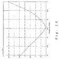
- FIG. 7 is the Smith chart of the first embodiment.
- FIG. 8 is the VSWR graph of the first embodiment.
- FIG. 9 is the azimuth field pattern of the electric field distribution of the second embodiment.
- FIG. 10 is the elevation field pattern of the electrical field distribution while ⁇ equals 0 of the second embodiment.
- FIG. 11 is the elevation field pattern of the electrical field distribution while ⁇ equals 90 degrees of the second embodiment.
- FIG. 12 is the return loss graph of the second embodiment.
- FIG. 13 is the Smith chart of the second embodiment.
- FIG. 14 is the VSWR graph of the second embodiment.
- FIG. 1 presents three views of the portable communication device of the preferred embodiment of the present invention.
- Such portable communication device comprises a dielectric substrate 1 , a radio module 2 , a ground plane 3 , a feed line 4 , a patch radiator 5 and an x-shaped coupled slot 6 .
- the antenna is deposited within a dielectric housing 7 , and the dielectric substrate 1 generally is a PCB with various electronic components and control circuits, which would be detailed in following description.
- the radio module is coupled on the surface of dielectric substrate.
- the feed line 4 is coupled to the dielectric substrate 1 on the same side with the radio module 2 .
- One terminal of the feed line 4 coupled to the radio module 2 , and the feed line 4 extends substantially toward the long axis of the dielectric substrate.
- the feed line 4 includes the stub, and the feed line feeds signals into the radio module 2 .
- the ground plane 3 is coupled to the dielectric substrate on the side other than that with radio module 2 .
- the ground plane 3 has the size substantially equal to that of the dielectric substrate, and generally constituted with conducting material, such as metal plate, for ground.
- the X-shaped coupled slot is formed on the ground plane 3 , and the feed line 4 passes through the intersection point of this X-shaped coupled slot.
- the feed line 4 is a transmission line for transferring radio-frequency signals.
- the patch radiator 5 is coupled to the inner surface of the dielectric housing 7 , and has the area slightly greater than that of the X-shaped coupled slot 6 . Beside, the patch radiator 5 is deposited substantially on the position of the X-shaped coupled slot 6 .
- the patch radiator 5 is constituted with a conducting plate, such as a metal plate, for transmitting signals. It has to be noted, an air gap 8 is thereby formed between the X-shaped coupled slot 6 and the patch radiator 5 and it is employed as the resonant cavity for radiating the radio-frequency signals.
- the area of the patch radiator 5 is about 12.4 ⁇ 22 mm 2
- the height of the dielectric housing 7 is about 0.747 ⁇ 0.0375 mm
- the thickness of the air gap 8 is about 6 ⁇ 0.3 mm.
- the area of the feed line is preferably about 20 ⁇ 1 mm 2
- the area of the stub of the feed line 4 is preferably about 7.4 ⁇ 1 mm 2 .
- the dimension of the dielectric substrate 1 is about 50 ⁇ 25 ⁇ 0.747 mm 3 and the dielectric constant of the dielectric substrate 1 is about 4.2.
- the area occupied by the ground plane 3 is about 50 ⁇ 25 mm 2
- the area of the coupled slot 6 is 1 ⁇ 10 mm 2
- the included angle of the coupled slot is substantially around 60 degrees.
- the dimension of the metallic shield of the radio module 2 is about 10 ⁇ 10 ⁇ 1.5 mm 3 .
- the thickness of the patch radiator 5 is about 1.4 mils per ounce metallic foil, and the thickness of the feed line 4 , the stub and the ground plane 3 is about 0.7 mils per 0.7 ounce metallic foil.
- the dielectric constant of the substrate 1 is about 4.2, typically, the dielectric constant of the air is about 1.0 and of the dielectric housing 7 is about 3-6.
- FIG. 3 is the Azimuth pattern of the electric field of the present embodiment.
- FIG. 4 and FIG. 5 is the elevation pattern of the electric field of the present embodiment, wherein ⁇ equals 0 or 90 degrees, respectively.
- the peak gain thereof would be about 4.05287 dB.
- the peak gain thereof would be about 3.28312 dB.
- the average gain is about 1.94938 dB as ⁇ of E-theta equals 0, and the average gain is about ⁇ 0.3202146 dB as ⁇ of E-theta equals 90 degrees.
- the return loss is about 40.14 dB as the frequency of the antenna is around 5.545 GHz.
- FIG. 7 shows the Smith chart and FIG. 8 is the VSWR graph of the first embodiment.
- the frequency coverage in 10 dB is about 1,276 MHz or 4.874-6.150 GHz
- the frequency coverage of the cover low and middle UNII bands is 5.15-5.35 GHz
- the frequency coverage of WRC band is 5.47-5.725 GHz
- the frequency coverage of ISM band is 5.725-5.85 GHz.
- FIG. 2 presents three views of the slot-coupled antenna according to one embodiment of the present invention. This embodiment is similar to the above one, so the redundant description would be omitted.
- the antenna is constituted with dielectric substrate 1 , ground plane 3 , patch radiator 5 , and 8-shaped coupled slot.
- the 8-shaped coupled slot 9 is configured on the ground plane 3 .
- the feed line 4 substantially passes through the intersection point of the 8-shaped coupled slot 9 , as shown in the front view in FIG. 2 .
- the feed line 4 is a signal line applied for transferring signals.
- the patch radiator 5 is coupled to the inner side of the dielectric housing 7 and has the area slightly greater than that of 8-shaped coupled slot 9 .
- the patch radiator 5 is deposited on the position of 8-shaped coupled slot 9 and usually formed by a conductive plate, such as metal plate.
- the air stratum 8 between the 8-shaped coupled slot 9 and patch radiator 5 is used as a resonant cavity for communication signals. Since the parameters of the antenna in this embodiment are quite similar to those of the former embodiment, related illustration is omitted.
- FIG. 9 presents the azimuth field pattern of the electric field distribution of the present embodiment.
- the field pattern would be symmetrical.
- the peak gain of antenna is 3.35003 dB and the average gain is 0.574541 dB as ⁇ of E-theta equals 0.
- FIG. 10 and FIG. 11 present the elevation field pattern of the electrical field distribution while ⁇ equals 0 and 90 degrees.
- the peak gain thereof would be about 4.1536 dB when ⁇ of E-theta equals 0, and the peak gain thereof would be about 3.35003 dB when ⁇ of E-theta equals 90 degrees.
- the average gain is about 1.94978 dB as ⁇ of E-theta equals 0, and the average gain is about ⁇ 0.243249 dB as ⁇ of E-theta equals 90 degrees.
- FIG. 13 is the Smith chart and FIG. 14 illustrates the VSWR graph of the present embodiment.
- the frequency coverage in 10 dB is about 1,322 MHz or 4.902-6.224 GHz
- the frequency coverage of the cover low and Middle UNII bands is about 5.15-5.35 GHz
- the frequency coverage of WRC band is 5.47-5.725 GHz
- the frequency coverage of ISM band is 5.725-5.85 GHz.
- the slot-coupled antenna module is mainly applied in the hand-held or portable communication device, particularly that compatible with WiFi standard and protocols. Since the ground plane of the antenna is provided with a slot-coupled configuration, the disposition flexibility as well as the assembly firmness would be much better than those of prior art. Besides, the slot-coupled antenna of the present invention possesses greater radiation performance as compared with prior art. The X-shaped and 8-shaped slot-coupled configuration could provide wider bandwidth as well as greater return loss than traditional I-shaped slot-coupled configuration. Additionally, the radiation efficiency of the antenna of the present invention is comparable with that of popular H-shaped slot-coupled antenna configuration.
Landscapes
- Engineering & Computer Science (AREA)
- Computer Networks & Wireless Communication (AREA)
- Physics & Mathematics (AREA)
- Electromagnetism (AREA)
- Waveguide Aerials (AREA)
- Details Of Aerials (AREA)
Abstract
Description
-
- (1) Common antenna is directly fixed or connected on the PCB. Therefore, the performance of the antenna will be influenced or interference by other components on the PCB, such as the battery, the keyboard, the LCD panel, the connector, the speaker, the lens, the microphone, the push bottom switch, the wire harness and the LED.
- (2) The antenna is usually directly disposed on the housing, and connected to the PCB by the cable or adapter. Consequently, there would be shortcomings, such as cable loss of transmission, non-reliability of cable connection, and difficult assembling and trouble-shooting.
- (3) Since the antenna is disposed outside the housing, the cable or adapter through the housing is utilized to connect the antenna to the PCB. Accordingly, the signals would lose or the surface of housing would be rugged and rough.
- (4) Since the antenna is disposed in a standalone and outside the housing, the cable or adapter through the housing is utilized to connect the antenna to the PCB. Accordingly, the signals would lose and better mounting knowledge is required.
Claims (18)
Applications Claiming Priority (3)
| Application Number | Priority Date | Filing Date | Title |
|---|---|---|---|
| TW095124188 | 2006-07-03 | ||
| TW095124188A TWI349395B (en) | 2006-07-03 | 2006-07-03 | A portable communication device with slot-coupled antenna module |
| TW95124188A | 2006-07-03 |
Publications (2)
| Publication Number | Publication Date |
|---|---|
| US20080001837A1 US20080001837A1 (en) | 2008-01-03 |
| US7724192B2 true US7724192B2 (en) | 2010-05-25 |
Family
ID=38876039
Family Applications (1)
| Application Number | Title | Priority Date | Filing Date |
|---|---|---|---|
| US11/802,027 Expired - Fee Related US7724192B2 (en) | 2006-07-03 | 2007-05-18 | Portable communication device with slot-coupled antenna module |
Country Status (2)
| Country | Link |
|---|---|
| US (1) | US7724192B2 (en) |
| TW (1) | TWI349395B (en) |
Cited By (3)
| Publication number | Priority date | Publication date | Assignee | Title |
|---|---|---|---|---|
| US20090256765A1 (en) * | 2008-04-09 | 2009-10-15 | National Taiwan University | Antenna |
| US20110193754A1 (en) * | 2007-01-04 | 2011-08-11 | Schlub Robert W | Handheld electronic devices with isolated antennas |
| US8872708B2 (en) | 2007-01-04 | 2014-10-28 | Apple Inc. | Antennas for handheld electronic devices |
Families Citing this family (11)
| Publication number | Priority date | Publication date | Assignee | Title |
|---|---|---|---|---|
| FI20055637A0 (en) * | 2005-12-02 | 2005-12-02 | Nokia Corp | Kaksipolarisaatio-microstrip patch antenna structure |
| KR100873441B1 (en) * | 2007-07-30 | 2008-12-11 | 삼성전자주식회사 | Slot antenna |
| US8111204B2 (en) * | 2008-01-31 | 2012-02-07 | Silicon Laboratories Inc. | Slot antenna for a circuit board ground plane |
| US8489162B1 (en) * | 2010-08-17 | 2013-07-16 | Amazon Technologies, Inc. | Slot antenna within existing device component |
| KR20130066705A (en) | 2010-10-12 | 2013-06-20 | 몰렉스 인코포레이티드 | Low impedance slot fed antenna |
| CN103259078B (en) | 2012-02-21 | 2016-06-29 | 华硕电脑股份有限公司 | wireless communication device |
| CN104752839A (en) * | 2015-04-28 | 2015-07-01 | 四川省韬光通信有限公司 | High-gain broadband coupling slat type micro-strip antenna |
| CN111490333A (en) | 2018-11-06 | 2020-08-04 | 华为终端有限公司 | Coupling antenna device and electronic equipment |
| US10770781B1 (en) * | 2019-02-26 | 2020-09-08 | Microsoft Technology Licensing, Llc | Resonant cavity and plate hybrid antenna |
| TW202221978A (en) | 2020-11-24 | 2022-06-01 | 和碩聯合科技股份有限公司 | Electronic device |
| CN115411501B (en) * | 2021-05-26 | 2024-12-31 | Oppo广东移动通信有限公司 | Antenna assembly and electronic equipment |
Citations (9)
| Publication number | Priority date | Publication date | Assignee | Title |
|---|---|---|---|---|
| US5706015A (en) * | 1995-03-20 | 1998-01-06 | Fuba Automotive Gmbh | Flat-top antenna apparatus including at least one mobile radio antenna and a GPS antenna |
| US6188369B1 (en) * | 1997-05-30 | 2001-02-13 | Hitachi, Ltd. | Tunable slot antenna with capacitively coupled slot island conductor for precise impedance adjustment |
| US6239750B1 (en) * | 1998-08-28 | 2001-05-29 | Telefonaltiebolaget Lm Ericsson (Publ) | Antenna arrangement |
| US6989793B2 (en) * | 2001-09-24 | 2006-01-24 | Thales Nederland B.V. | Patch fed printed antenna |
| US20070296634A1 (en) * | 2005-03-09 | 2007-12-27 | Fraunhofer-Gesellschaft Zur Foerderung Der Angewandten Forschung E.V. | Aperture-coupled antenna |
| US7358920B2 (en) * | 2003-04-03 | 2008-04-15 | Bae Systems Information And Electronic Systems Integration Inc. | Cavity embedded antenna |
| US7389129B2 (en) * | 2002-11-06 | 2008-06-17 | Sony Ericsson Mobile Communications Japan, Inc. | Wireless communication apparatus |
| US7391381B2 (en) * | 2004-01-07 | 2008-06-24 | Motia | Vehicle mounted satellite antenna system with in-motion tracking using beam forming |
| US7471248B2 (en) * | 2005-03-09 | 2008-12-30 | Fraunhofer-Gesellschaft Zur Foerderung Der Angewandten Forschung E.V. | Planar multiband antenna |
-
2006
- 2006-07-03 TW TW095124188A patent/TWI349395B/en not_active IP Right Cessation
-
2007
- 2007-05-18 US US11/802,027 patent/US7724192B2/en not_active Expired - Fee Related
Patent Citations (9)
| Publication number | Priority date | Publication date | Assignee | Title |
|---|---|---|---|---|
| US5706015A (en) * | 1995-03-20 | 1998-01-06 | Fuba Automotive Gmbh | Flat-top antenna apparatus including at least one mobile radio antenna and a GPS antenna |
| US6188369B1 (en) * | 1997-05-30 | 2001-02-13 | Hitachi, Ltd. | Tunable slot antenna with capacitively coupled slot island conductor for precise impedance adjustment |
| US6239750B1 (en) * | 1998-08-28 | 2001-05-29 | Telefonaltiebolaget Lm Ericsson (Publ) | Antenna arrangement |
| US6989793B2 (en) * | 2001-09-24 | 2006-01-24 | Thales Nederland B.V. | Patch fed printed antenna |
| US7389129B2 (en) * | 2002-11-06 | 2008-06-17 | Sony Ericsson Mobile Communications Japan, Inc. | Wireless communication apparatus |
| US7358920B2 (en) * | 2003-04-03 | 2008-04-15 | Bae Systems Information And Electronic Systems Integration Inc. | Cavity embedded antenna |
| US7391381B2 (en) * | 2004-01-07 | 2008-06-24 | Motia | Vehicle mounted satellite antenna system with in-motion tracking using beam forming |
| US20070296634A1 (en) * | 2005-03-09 | 2007-12-27 | Fraunhofer-Gesellschaft Zur Foerderung Der Angewandten Forschung E.V. | Aperture-coupled antenna |
| US7471248B2 (en) * | 2005-03-09 | 2008-12-30 | Fraunhofer-Gesellschaft Zur Foerderung Der Angewandten Forschung E.V. | Planar multiband antenna |
Cited By (5)
| Publication number | Priority date | Publication date | Assignee | Title |
|---|---|---|---|---|
| US20110193754A1 (en) * | 2007-01-04 | 2011-08-11 | Schlub Robert W | Handheld electronic devices with isolated antennas |
| US8872708B2 (en) | 2007-01-04 | 2014-10-28 | Apple Inc. | Antennas for handheld electronic devices |
| US8907850B2 (en) * | 2007-01-04 | 2014-12-09 | Apple Inc. | Handheld electronic devices with isolated antennas |
| US20090256765A1 (en) * | 2008-04-09 | 2009-10-15 | National Taiwan University | Antenna |
| US8207903B2 (en) * | 2008-04-09 | 2012-06-26 | National Taiwan University | Antenna |
Also Published As
| Publication number | Publication date |
|---|---|
| TWI349395B (en) | 2011-09-21 |
| US20080001837A1 (en) | 2008-01-03 |
| TW200805784A (en) | 2008-01-16 |
Similar Documents
| Publication | Publication Date | Title |
|---|---|---|
| US7724192B2 (en) | Portable communication device with slot-coupled antenna module | |
| CN112151962B (en) | Electronic device with multi-frequency ultra-wideband antenna | |
| US7764236B2 (en) | Broadband antenna for handheld devices | |
| AU2008205147B2 (en) | Antennas for handheld electronic devices | |
| CN203589190U (en) | An electronic device with an antenna | |
| US6424300B1 (en) | Notch antennas and wireless communicators incorporating same | |
| EP2083472A1 (en) | Antenna isolation for portable electronic devices | |
| EP4027453B1 (en) | Antenna structure and electronic device | |
| CN113594687B (en) | Antenna module and electronic equipment | |
| US7372411B2 (en) | Antenna arrangement and method for making the same | |
| US7199756B2 (en) | Planar antenna for wireless communication device and portable computer using the same | |
| US7940218B2 (en) | Multilayer PCB antenna | |
| KR20010003035A (en) | Printing-Type Inverted F Antenna | |
| US20060139214A1 (en) | Antenna | |
| CN100399625C (en) | Concealed antenna | |
| US6999031B2 (en) | Antenna device and its use in a communication device | |
| US7193580B2 (en) | Antenna device | |
| US20040222928A1 (en) | Multi-frequency antenna module for a portable electronic apparatus | |
| US11011855B2 (en) | Antenna system | |
| CN101154768B (en) | Handheld communication device with coupled slot antenna module | |
| CN215989221U (en) | Antenna device and electronic apparatus | |
| US7064715B2 (en) | Antenna module for an electronic apparatus | |
| US8044860B2 (en) | Internal antenna for mobile device | |
| CN120749400A (en) | Low-profile miniaturized reader antenna | |
| CN119422287A (en) | Antenna assembly with directional antenna for communication device |
Legal Events
| Date | Code | Title | Description |
|---|---|---|---|
| AS | Assignment |
Owner name: ACCTON TECHNOLOGY CORPORATION, TAIWAN Free format text: ASSIGNMENT OF ASSIGNORS INTEREST;ASSIGNOR:LIU, I-RU;REEL/FRAME:019392/0930 Effective date: 20070423 Owner name: ACCTON TECHNOLOGY CORPORATION,TAIWAN Free format text: ASSIGNMENT OF ASSIGNORS INTEREST;ASSIGNOR:LIU, I-RU;REEL/FRAME:019392/0930 Effective date: 20070423 |
|
| STCF | Information on status: patent grant |
Free format text: PATENTED CASE |
|
| FPAY | Fee payment |
Year of fee payment: 4 |
|
| MAFP | Maintenance fee payment |
Free format text: PAYMENT OF MAINTENANCE FEE, 8TH YEAR, LARGE ENTITY (ORIGINAL EVENT CODE: M1552) Year of fee payment: 8 |
|
| FEPP | Fee payment procedure |
Free format text: MAINTENANCE FEE REMINDER MAILED (ORIGINAL EVENT CODE: REM.); ENTITY STATUS OF PATENT OWNER: LARGE ENTITY |
|
| LAPS | Lapse for failure to pay maintenance fees |
Free format text: PATENT EXPIRED FOR FAILURE TO PAY MAINTENANCE FEES (ORIGINAL EVENT CODE: EXP.); ENTITY STATUS OF PATENT OWNER: LARGE ENTITY |
|
| STCH | Information on status: patent discontinuation |
Free format text: PATENT EXPIRED DUE TO NONPAYMENT OF MAINTENANCE FEES UNDER 37 CFR 1.362 |
|
| FP | Lapsed due to failure to pay maintenance fee |
Effective date: 20220525 |