US7715457B2 - High power semiconductor laser diode - Google Patents
High power semiconductor laser diode Download PDFInfo
- Publication number
- US7715457B2 US7715457B2 US12/094,316 US9431606A US7715457B2 US 7715457 B2 US7715457 B2 US 7715457B2 US 9431606 A US9431606 A US 9431606A US 7715457 B2 US7715457 B2 US 7715457B2
- Authority
- US
- United States
- Prior art keywords
- ridge
- section
- laser diode
- separate
- diode according
- Prior art date
- Legal status (The legal status is an assumption and is not a legal conclusion. Google has not performed a legal analysis and makes no representation as to the accuracy of the status listed.)
- Active, expires
Links
- 239000004065 semiconductor Substances 0.000 title claims abstract description 28
- 239000000969 carrier Substances 0.000 claims abstract description 8
- 229910000980 Aluminium gallium arsenide Inorganic materials 0.000 claims abstract description 6
- 238000000926 separation method Methods 0.000 claims abstract description 5
- 238000002955 isolation Methods 0.000 claims description 16
- 238000004519 manufacturing process Methods 0.000 claims description 15
- 238000000034 method Methods 0.000 claims description 11
- 238000002347 injection Methods 0.000 claims description 7
- 239000007924 injection Substances 0.000 claims description 7
- 238000001465 metallisation Methods 0.000 claims description 7
- 229910001218 Gallium arsenide Inorganic materials 0.000 claims description 2
- 229910000530 Gallium indium arsenide Inorganic materials 0.000 claims 1
- 238000003486 chemical etching Methods 0.000 claims 1
- 238000000151 deposition Methods 0.000 claims 1
- 238000009792 diffusion process Methods 0.000 claims 1
- 229910052814 silicon oxide Inorganic materials 0.000 claims 1
- 230000003287 optical effect Effects 0.000 abstract description 27
- 238000013461 design Methods 0.000 abstract description 22
- 230000015556 catabolic process Effects 0.000 abstract description 8
- 238000006731 degradation reaction Methods 0.000 abstract description 8
- 239000000835 fiber Substances 0.000 abstract description 5
- 230000006872 improvement Effects 0.000 abstract description 5
- 238000004891 communication Methods 0.000 abstract description 4
- 230000007774 longterm Effects 0.000 abstract description 2
- 230000005693 optoelectronics Effects 0.000 abstract description 2
- 241000217377 Amblema plicata Species 0.000 abstract 1
- 239000000463 material Substances 0.000 description 9
- 230000008569 process Effects 0.000 description 9
- 238000012545 processing Methods 0.000 description 8
- 238000001914 filtration Methods 0.000 description 6
- 238000013459 approach Methods 0.000 description 5
- 238000009826 distribution Methods 0.000 description 5
- 230000008901 benefit Effects 0.000 description 4
- 238000005253 cladding Methods 0.000 description 4
- 230000007480 spreading Effects 0.000 description 4
- 238000003892 spreading Methods 0.000 description 4
- 230000000694 effects Effects 0.000 description 3
- 238000005530 etching Methods 0.000 description 3
- 238000010521 absorption reaction Methods 0.000 description 2
- 238000006243 chemical reaction Methods 0.000 description 2
- 239000013078 crystal Substances 0.000 description 2
- 239000006185 dispersion Substances 0.000 description 2
- 238000005516 engineering process Methods 0.000 description 2
- 238000010438 heat treatment Methods 0.000 description 2
- 230000004048 modification Effects 0.000 description 2
- 238000012986 modification Methods 0.000 description 2
- 238000000059 patterning Methods 0.000 description 2
- 238000005215 recombination Methods 0.000 description 2
- 230000006798 recombination Effects 0.000 description 2
- 239000011343 solid material Substances 0.000 description 2
- 239000000243 solution Substances 0.000 description 2
- 230000004083 survival effect Effects 0.000 description 2
- 229910052691 Erbium Inorganic materials 0.000 description 1
- 229910002601 GaN Inorganic materials 0.000 description 1
- 229910005542 GaSb Inorganic materials 0.000 description 1
- 208000012868 Overgrowth Diseases 0.000 description 1
- 230000006978 adaptation Effects 0.000 description 1
- 230000003321 amplification Effects 0.000 description 1
- 230000000903 blocking effect Effects 0.000 description 1
- 230000008859 change Effects 0.000 description 1
- 238000000576 coating method Methods 0.000 description 1
- 238000005520 cutting process Methods 0.000 description 1
- 238000001312 dry etching Methods 0.000 description 1
- UYAHIZSMUZPPFV-UHFFFAOYSA-N erbium Chemical compound [Er] UYAHIZSMUZPPFV-UHFFFAOYSA-N 0.000 description 1
- 238000005297 material degradation process Methods 0.000 description 1
- 238000005259 measurement Methods 0.000 description 1
- 229910052751 metal Inorganic materials 0.000 description 1
- 239000002184 metal Substances 0.000 description 1
- 238000003199 nucleic acid amplification method Methods 0.000 description 1
- 239000013307 optical fiber Substances 0.000 description 1
- 238000004806 packaging method and process Methods 0.000 description 1
- 238000002161 passivation Methods 0.000 description 1
- 238000005086 pumping Methods 0.000 description 1
- 230000005855 radiation Effects 0.000 description 1
- 230000009467 reduction Effects 0.000 description 1
- 239000000758 substrate Substances 0.000 description 1
- 238000012360 testing method Methods 0.000 description 1
- 238000001039 wet etching Methods 0.000 description 1
Images


Classifications
-
- H—ELECTRICITY
- H01—ELECTRIC ELEMENTS
- H01S—DEVICES USING THE PROCESS OF LIGHT AMPLIFICATION BY STIMULATED EMISSION OF RADIATION [LASER] TO AMPLIFY OR GENERATE LIGHT; DEVICES USING STIMULATED EMISSION OF ELECTROMAGNETIC RADIATION IN WAVE RANGES OTHER THAN OPTICAL
- H01S5/00—Semiconductor lasers
- H01S5/20—Structure or shape of the semiconductor body to guide the optical wave ; Confining structures perpendicular to the optical axis, e.g. index or gain guiding, stripe geometry, broad area lasers, gain tailoring, transverse or lateral reflectors, special cladding structures, MQW barrier reflection layers
- H01S5/22—Structure or shape of the semiconductor body to guide the optical wave ; Confining structures perpendicular to the optical axis, e.g. index or gain guiding, stripe geometry, broad area lasers, gain tailoring, transverse or lateral reflectors, special cladding structures, MQW barrier reflection layers having a ridge or stripe structure
-
- H—ELECTRICITY
- H01—ELECTRIC ELEMENTS
- H01S—DEVICES USING THE PROCESS OF LIGHT AMPLIFICATION BY STIMULATED EMISSION OF RADIATION [LASER] TO AMPLIFY OR GENERATE LIGHT; DEVICES USING STIMULATED EMISSION OF ELECTROMAGNETIC RADIATION IN WAVE RANGES OTHER THAN OPTICAL
- H01S5/00—Semiconductor lasers
- H01S5/10—Construction or shape of the optical resonator, e.g. extended or external cavity, coupled cavities, bent-guide, varying width, thickness or composition of the active region
- H01S5/16—Window-type lasers, i.e. with a region of non-absorbing material between the active region and the reflecting surface
-
- H—ELECTRICITY
- H01—ELECTRIC ELEMENTS
- H01S—DEVICES USING THE PROCESS OF LIGHT AMPLIFICATION BY STIMULATED EMISSION OF RADIATION [LASER] TO AMPLIFY OR GENERATE LIGHT; DEVICES USING STIMULATED EMISSION OF ELECTROMAGNETIC RADIATION IN WAVE RANGES OTHER THAN OPTICAL
- H01S5/00—Semiconductor lasers
- H01S5/06—Arrangements for controlling the laser output parameters, e.g. by operating on the active medium
- H01S5/065—Mode locking; Mode suppression; Mode selection ; Self pulsating
- H01S5/0651—Mode control
- H01S5/0653—Mode suppression, e.g. specific multimode
- H01S5/0655—Single transverse or lateral mode emission
-
- H—ELECTRICITY
- H01—ELECTRIC ELEMENTS
- H01S—DEVICES USING THE PROCESS OF LIGHT AMPLIFICATION BY STIMULATED EMISSION OF RADIATION [LASER] TO AMPLIFY OR GENERATE LIGHT; DEVICES USING STIMULATED EMISSION OF ELECTROMAGNETIC RADIATION IN WAVE RANGES OTHER THAN OPTICAL
- H01S5/00—Semiconductor lasers
- H01S5/10—Construction or shape of the optical resonator, e.g. extended or external cavity, coupled cavities, bent-guide, varying width, thickness or composition of the active region
- H01S5/1003—Waveguide having a modified shape along the axis, e.g. branched, curved, tapered, voids
- H01S5/1014—Tapered waveguide, e.g. spotsize converter
-
- H—ELECTRICITY
- H01—ELECTRIC ELEMENTS
- H01S—DEVICES USING THE PROCESS OF LIGHT AMPLIFICATION BY STIMULATED EMISSION OF RADIATION [LASER] TO AMPLIFY OR GENERATE LIGHT; DEVICES USING STIMULATED EMISSION OF ELECTROMAGNETIC RADIATION IN WAVE RANGES OTHER THAN OPTICAL
- H01S5/00—Semiconductor lasers
- H01S5/10—Construction or shape of the optical resonator, e.g. extended or external cavity, coupled cavities, bent-guide, varying width, thickness or composition of the active region
- H01S5/1003—Waveguide having a modified shape along the axis, e.g. branched, curved, tapered, voids
- H01S5/1017—Waveguide having a void for insertion of materials to change optical properties
-
- H—ELECTRICITY
- H01—ELECTRIC ELEMENTS
- H01S—DEVICES USING THE PROCESS OF LIGHT AMPLIFICATION BY STIMULATED EMISSION OF RADIATION [LASER] TO AMPLIFY OR GENERATE LIGHT; DEVICES USING STIMULATED EMISSION OF ELECTROMAGNETIC RADIATION IN WAVE RANGES OTHER THAN OPTICAL
- H01S5/00—Semiconductor lasers
- H01S5/10—Construction or shape of the optical resonator, e.g. extended or external cavity, coupled cavities, bent-guide, varying width, thickness or composition of the active region
- H01S5/1082—Construction or shape of the optical resonator, e.g. extended or external cavity, coupled cavities, bent-guide, varying width, thickness or composition of the active region with a special facet structure, e.g. structured, non planar, oblique
-
- H—ELECTRICITY
- H01—ELECTRIC ELEMENTS
- H01S—DEVICES USING THE PROCESS OF LIGHT AMPLIFICATION BY STIMULATED EMISSION OF RADIATION [LASER] TO AMPLIFY OR GENERATE LIGHT; DEVICES USING STIMULATED EMISSION OF ELECTROMAGNETIC RADIATION IN WAVE RANGES OTHER THAN OPTICAL
- H01S5/00—Semiconductor lasers
- H01S5/30—Structure or shape of the active region; Materials used for the active region
- H01S5/32—Structure or shape of the active region; Materials used for the active region comprising PN junctions, e.g. hetero- or double- heterostructures
- H01S5/323—Structure or shape of the active region; Materials used for the active region comprising PN junctions, e.g. hetero- or double- heterostructures in AIIIBV compounds, e.g. AlGaAs-laser, InP-based laser
Definitions
- the present invention relates to semiconductor laser diodes, particularly to AlGaAs-based laser diodes of high light output power.
- Such laser diodes are commonly used in opto-electronics, often as so-called pump lasers for fiber amplifiers in the field of optical communications systems, e.g. for Erbium-doped fiber amplifiers.
- ridge waveguide laser diodes are suited to provide the desired narrow-bandwidth optical radiation with a stable light output power in a given frequency band. Output power and stability of such laser diodes are of crucial interest and any degradation during normal use must be avoided.
- the present invention concerns an improved design of such laser diodes, the improvement in particular significantly minimizing or avoiding, compared to prior art designs, front facet degradation of such laser diodes at high light output powers.
- the present invention further concerns an improved design of such laser diodes in which substantially separate electrical control can be applied to a section of such a laser, preferably adjacent to a facet.
- Semiconductor laser diodes of the type mentioned above have, for example, become important components in the technology of optical communication, particularly because such laser diodes can be used for amplifying optical signals immediately by optical means, thereby avoiding any complicated conversion of transmitted signals along the route between the transmitter and receiver, and thus improving speed and reliability within such systems.
- laser diodes are used for pumping Erbium-doped fiber amplifiers, so-called EDFAs, which have been described in various patents and publications known to the person skilled in the art.
- EDFAs Erbium-doped fiber amplifiers
- ridge-waveguide laser diodes with a power output of 150 mW or more, whose wavelengths match the erbium absorption lines and provide low-noise amplification.
- Several laser diodes have been found to serve this purpose well and are used today in significant numbers.
- One of the major problems of semiconductor laser diodes of the types mentioned above is degradation of the waveguide adjacent to a facet, in particular at the front facet of the laser. This degradation is believed to be caused by temperature increase at the mirror facet regions, especially at high power outputs, which temperature increase in turn is probably caused by unwanted carrier recombination in these regions and heating due to free carrier injection.
- Such approaches typically comprise providing current blocking regions above the ridge of a ridge waveguide laser, adjacent to the facet.
- Schmidt et al. U.S. Pat. No. 6,782,024, assigned to the assignee of the present invention and incorporated herein by reference, is an example of a solution to the above-identified problem. It discloses a semiconductor ridge-waveguide laser diode with means for limiting the injection of carriers at one or both of the diode's end sections, thus providing at least one “unpumped” end section.
- This injection limiting means comprises an isolation layer which extends at least partially over the end sections and inhibits the injection of carriers from the usual metallization into the active region of the laser diode.
- Other examples of such approaches are given by Yu et al. in U.S. Pat. No. 6,373,875 and Sagawa et al. in U.S. Pat. No. 5,844,931.
- a semiconductor ridge waveguide laser diode including a semiconductor body, a ridge on a surface of the semiconductor body defining a waveguide between first and second facets, a first electrode on the ridge for injecting carriers into the laser diode, a second electrode located on a surface of the semiconductor body opposite to the surface having the ridge, characterized in that the ridge comprises a plurality of regions, including a main ridge section and a separate ridge section, separated by a physical separator, such as a trench, passing through at least a part of the height of the ridge.
- the present invention provides a ridge waveguide laser diode with a passive section of the ridge waveguide by providing a trench or gap between at least the active main section of the laser diode ridge (i.e. the main ridge section) and a separate smaller part of the ridge adjacent to a facet of the laser diode (i.e. the separate ridge section).
- the drive electrode on the main ridge section does not extend to cover the separate ridge section, which consequently forms a passive separate ridge section, i.e. a section into which substantially no current spreads.
- Two trenches, one towards the front facet and one towards the rear facet, may be provided if it is desired to provide two passive separate ridge sections.
- the invention also concerns an appropriate manufacturing process for making such a trench by etching it into the ridge waveguide of a high power laser diode.
- the result is a very high power laser diode with a reduced susceptibility to failure, in particular by substantially eliminating any current density in the separate section of the ridge waveguide adjacent to the end facet, due to current injection through the electrode on the main ridge section, thus displaying increased reliability compared with prior art devices.
- the increased device reliability is due to the novel “separate ridge section” design, which differs significantly from the known unpumped end section design.
- the physical separator is preferably a trench empty of solid material, the entire ridge, including the trench, may be overgrown by solid material in the case where the device is a buried ridge device. Alternatively passivation material may be grown in the trench.
- the physical separator provides a refractive index contrast, and, although the greatest contrast would be provided by a semiconductor-air boundary, the use in the physical separator of a dissimilar overgrowth material may still provide a sufficient though reduced contrast.
- a trench or gap is etched across the width of the laser's ridge, either as part of the ridge etch process, or as a separate etch step, resulting in a passive ridge waveguide end section, i.e. an end section into which substantially no current can diffuse.
- the current may simply be reduced to a low level.
- the trench cuts through the top contact layer of highly doped semiconductor material, that is typically present, and into the less conductive, less highly doped region of upper cladding beneath. This cutting through of the contact layer has a disproportionate effect on reducing the current flow into the separate ridge section.
- the separate ridge section may act as a spatial mode filter, i.e. a filter generating higher absorption losses for higher order optical modes. This is due to both the trench and the passive separate ridge section, in the case that the ridge of the end section is narrower than that of the main body of the ridge, and thus reduces the negative impact of non-Gaussian or non-centered light reflected back from the output facet or coupled back into the ridge waveguide, e.g. from a fiber Bragg grating.
- the separate section of the ridge waveguide may be shaped in different ways, which, since no current is injected from the electrode on the main ridge section, removes a significant design limitation for this section of the ridge waveguide.
- the novel technology can be applied to narrow stripe laser diodes as well as to broad area semiconductor laser diodes. Possible design variations are shown in the appended drawings and described in the following sections of this specification.
- a ridge waveguide laser diode structured according to the present invention provides a substantially separate ridge section, which exhibits a significant improvement over prior art laser diodes with partially unpumped end sections, especially with regard to its long-term stability and reliability.
- a laser diode according to the invention may also provide an increased power output compared to a prior art design. Further, it may be possible to reduce the size of such a novel laser diode and still provide the same or even an increased output.
- This significant improvement may be effected by just a minor increase in manufacturing complexity so that conventional manufacturing equipment may be used and usual manufacturing processes may be applied. Also, the laser diode itself may have approximately the same dimensions as before, thus avoiding any packaging changes or problems.
- the design idea of one or two separate ridge section(s) adjacent to the end facets of a ridge waveguide laser diode serves to reduce carrier concentration close to the facets.
- the regions adjacent to the mirror are usually the weak points in terms of reliability.
- the invention provides a solution by establishing one, two or more separate, passive ridge section(s), thus significantly reducing the failure rate at very high optical output powers, particularly in the front facet region.
- control electrode provided on the separate ridge section of the ridge waveguide laser diode.
- the advantage of providing such an electrode is that separate electrical control may be applied to the separate ridge section of the laser, since the trench substantially prevents current through said section from spreading into the main body of the device.
- the invention is not limited to high power laser diodes, but is applicable to any ridge waveguide laser diode, e.g. to narrow stripe or broad area laser diodes with a ridge waveguide structure.
- ridge waveguide laser diode e.g. to narrow stripe or broad area laser diodes with a ridge waveguide structure.
- the person skilled in the art will know how to modify the details given below to adapt the present invention to such other laser diodes.
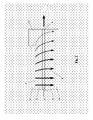
- FIG. 1 a schematic, perspective, “exploded” view of the structure of a prior art ridge waveguide laser diode
- FIG. 2 the current distribution in a schematic cross section of a prior art ridge waveguide laser diode, adjacent to the front facet;
- FIG. 3 the current distribution in a schematic cross section of a ridge waveguide laser diode according to the present invention, adjacent to the front facet;
- FIGS. 4 a - 4 h schematic, perspective views of several laser diodes according to the present invention.
- FIGS. 5 a , 5 b a schematic plan view of the use of the invention in a specific design of a cleaved laser
- FIG. 6 a graph showing simulated losses for the zero order mode and the first order mode of a laser diode according to the invention.
- FIG. 7 a graph comparing failures of a prior art laser diode with failures of a laser diode according to the invention.
- the invention aims to reduce the local current density within the laser's end sections to reduce the degradation caused and accelerated by local heating of the laser.
- the local current in the end section of a prior art laser is—as is the current in other parts of the laser diode—substantially generated by the injection current driving the laser diode.
- the current injected into these end sections must be reduced.
- Various processes have been tested, including contact lift-off, removing the contact by etching, or otherwise interrupting the contact around these regions.
- many of the processes tested and realized failed due to material, processing, or reliability problems or were just too complicated to be commercially viable.
- FIG. 1 depicting an AlGaAs ridge waveguide laser diode in a perspective and partially exploded view.
- This 980 nm pump laser diode consists of a SQW (strained quantum well) active region 7 sandwiched by two AlGaAs cladding layers 2 and 3 .
- the top electrode 6 covers the semiconductor ridge 4 together with the embedding material 5 .
- At the bottom of the body 1 is an n-metallization 14 .
- the additional isolation layers 11 , 13 here made of SiN, are located between the top metallization 6 and the AlGaAs active region layer 2 , and extend across the ridge 4 adjacent to the end facets.
- the unpumped end section is established by careful alignment of the additional isolation layers 11 and 13 , respectively, on top and around the ridge 4 .
- the isolation layers 11 and 13 may extend laterally over the whole width of the semiconductor body 1 . They are formed in a separate process, wherein an applied isolation layer is patterned using a lithographic mask process and an etching step, after definition of the further, lateral isolation layers 5 as self-aligned layers around the ridge waveguide on top of the semiconductor body 1 .
- any of the isolation layers 11 and 13 may be of different thickness and/or material as compared to the further isolation layers 5 .
- the electrode 6 covers the whole device and provides the driving current for the laser diode.
- FIG. 1 The person skilled in the art knows that some parts of a functioning laser diode are not shown in FIG. 1 , e.g. the front and rear mirror coatings, the leads providing the current to the electrodes, i.e. the electrodes 6 and 14 , etc. But these parts are rather standard and are not shown here for the sake of clarity.
- FIG. 2 shows schematically the current distribution along a vertical cross section along the length of a prior art ridge waveguide laser diode according to FIG. 1 , i.e. with an unpumped end section.
- An isolation layer 11 is provided between the top metallization 6 and the ridge 4 adjacent to the end facet 8 , and thus produces a current distribution approximately as indicated by the arrows 9 .
- the laser light exits the front facet 8 of the laser, and is depicted by an arrow. The remaining parts are equivalent to those shown in FIG. 1 .
- FIG. 3 shows, again schematically and in the same scale as FIG. 2 , the basic concept of the invention.
- a trench (or gap) 10 separates the active, main ridge section 4 , which comprises the main body of the ridge and is covered by the top metallization 6 , from a passive, separate ridge section 12 .
- the physical separation between the two ridge sections results in a significantly changed current pattern, as indicated by the arrows 9 , in which there is substantially no current flowing through the region of the laser diode adjacent to the facet.
- this trench 10 may be arranged at the laser's front facet, or at the laser's rear facet, or at both ends of the laser. Further, the gap may be modified in its depth, its width, its form, or all of them to suit the desired effect. Even further, modification of the separate ridge section 12 regarding its length, its width, or its shape may be advisable, as will be shown and explained, below.
- FIG. 4 a shows a perspective view of a ridge waveguide laser diode according to a first embodiment of the present invention (which corresponds with the cross section shown in FIG. 3 ) in which a passive, separate ridge section 12 is separated from an active ridge section 4 by trench 10 .
- Electrodes 6 and 14 are provided on the active main ridge section 4 and the substrate surface opposite to the ridge respectively for supplying a drive current to the laser diode. Light is created due to optical gain and shown by optical mode 15 .
- Passive, separate ridge section 12 has the same width and form as the active main ridge section 4 .
- the trench 10 is etched to a depth equal to the height of the ridge above the adjoining surface, and may advantageously be etched in the same etch step as the ridge.
- the trench 10 is etched in a different etch step to the ridge, and may be etched more or less deeply, as is illustrated in FIGS. 4 b and 4 c respectively, from which the electrodes 6 , 14 have been omitted for clarity (similarly from FIGS. 4 c , 4 d and 4 e ).
- FIG. 4 d shows a laser diode that is similar to that of FIG. 4 a , except that the passive ridge end section 112 is narrower than the active main ridge section 4 .
- Such a design may advantageously provide spatial filtering, which has particular application in the case of a single mode laser diode by suppressing higher order optical modes preferentially, relative to the fundamental optical mode.
- An exemplary width of the active main ridge section 4 for a typical single-mode, narrow-stripe laser diode is around 5 ⁇ m.
- the narrowed passive end section 112 may have a reduced width of about 3-4 ⁇ m.
- the active ridge is usually wider, e.g. up to 200 ⁇ m.
- the passive end section may be higher or lower than the active main ridge section (not illustrated).
- the preferred design is a narrower separate ridge section, which provides spatial filtering of higher order modes, in the preferred case of a single mode laser.
- Higher order modes have a wider lateral extent, and so lateral features that introduce loss provide a larger effect on higher order modes than on the fundamental mode.
- the reduction in ridge width of the separate section 112 of FIG. 4 d will preferentially laterally ‘clip’ the tops (for a weakly guiding waveguide) of any unwanted higher order modes. Even quite modest increases in optical loss can be adequate to help differentiate between modes and ensure that the laser lases on the fundamental mode.
- Ridge sections with different widths can be easily incorporated into a design, simply by changing the width of the features that define the ridge width on the corresponding lithographic mask.
- dissimilar ridge widths can be introduced without introducing extra processing steps (although the addition of the trench etch typically introduces extra processing steps, unless it is also incorporated into the mask that defines the ridge widths, which produce a trench of the same depth as the ridge height).
- each of the ridge sections described above is of constant width and height along its length, it is also within the scope of the invention for the width and height of the section to vary along along its length, for example by being evenly tapered in height or width along its length. In this case the mean width and height of the ridge sections may be compared.
- Spreading or constriction by tapering is ideally adiabatic, but in practice will typically introduce a small amount of unwanted mode conversion. Since light in a laser cavity moves in both directions along the waveguide, it experiences both spreading and constriction.
- the separate ridge section 12 may be wider than the ridge of the active main ridge section 4 . If, e.g., an improved cleaving quality is desired and/or the dispersion of the beam is less important for a specific application of the laser diode, the width of the passive end section may even be a multiple of the width of the active main ridge section 4 , both for single-mode or multi-mode laser diodes, respectively. Such a design is shown in FIG. 4 e.
- the laser diode may have separate sections 12 , 212 adjacent to each end facet and separated from the active main ridge section 4 by respective trenches 10 , 110 , as is shown in FIG. 4 f.
- FIG. 4 g shows an embodiment of the present invention in which a trench 10 separates the active main ridge section 4 from an end section 312 , on which there is provided a control electrode 20 to supply current to the separate ridge section 312 .
- the trench 10 enables substantially independent control of the currents in the active main ridge section 4 and end section 312 .
- the control electrode 20 may be electrically connected to electrode 14 or reverse biased with respect to the bias applied to the active main ridge section 4 by electrodes 6 and 14 , e.g. to further reduce any low level current that may be flowing through the active layer 7 within the section of the waveguide beneath separate ridge section 312 , resulting in potential further benefits to reliability and waveguide stability.
- control electrode 20 may be forward biased at a lower level than electrode 6 , with respect to electrode 14 , such as to produce optical gain in the separate section 312 .
- end section electrode 20 may be biased such that the laser diode operates in a manner that is self-pulsing.
- a plurality of separate ridge sections are provided between the main active ridge section 4 and an end facet 8 , of which one section is narrower to provide spatial filtering.
- FIG. 4 h shows such an embodiment, in which an active separate ridge section 412 and a passive separate ridge section 512 are separated from the active main ridge section 4 and each other by two trenches 10 , 210 , the spatial filtering being provided by the separate ridge section 512 adjacent to the facet.
- the neighbouring separate ridge section 412 could be narrower to provide spatial filtering. Any or none of the separate ridge sections may be provided with a control electrode.
- the separate ridge sections shown in FIGS. 4 a - h have the same length, but this need not to be the case.
- the length of a separate ridge section may be up to 500 ⁇ m.
- the desired balance between the optical loss in the passive separate ridge section versus the desired output of the laser diode determines the length of the passive ridge section, either alone or in combination with any of the measures described above.
- An exemplary trench length (i.e. the distance between the active main ridge section 4 and a separate ridge section, e.g. 12) is between 2 and 100 ⁇ m, and preferably between 5 and 20 ⁇ m. Trench lengths down to 5 ⁇ m can be easily manufactured by wet etching. Shorter trenches, e.g. down to 2 ⁇ m, may be manufactured by dry etching.
- the trenches (e.g. 10 , 110 ) are shown in FIGS. 4 a to 4 h as having the same length.
- the dispersion of the optical beam exiting the laser diode is affected.
- a greater gap length reduces the percentage of the zero order optical mode coupled into the separate ridge section(s).
- the upper limit however is determined by the desired efficiency and stability of the laser diode, since optical losses increase with increasing trench length.
- the invention is applicable to all high power semiconductor laser diodes and is independent of the base material used, e.g. InP, GaAs, GaN, GaSb, etc.
- the only requirement is that the internal losses of the base material are approximately 1-2 cm ⁇ 1 , or less.
- FIGS. 5 a and 5 b show an example of a single-mode semiconductor laser diode design which, as will be shown, is particularly suitable for implementation of the present invention.
- a laser diode according to Schmidt et al. U.S. Pat. No. 6,798,815 is usually manufactured by placing and processing several hundred laser diodes on a semiconductor waver. All laser diodes are identical and oriented in the same direction end-to-end all over the wafer.
- FIG. 5 a shows a single laser diode, which is representative of the repeating design on a whole wafer.
- FIG. 5 b shows two laser diodes and the line 16 along which these two laser diodes are divided by cleaving.
- a separate ridge section may be used that is tapered, and is narrower in such a way that it provides spatial filtering, and yet has the same width at the output facet as the main ridge section. This has the advantage of ease of manufacturing, so that devices may be cleaved from a bar comprising nose-to-tail devices.
- FIG. 6 is a graph comparing simulated losses for the zero order optical mode, solid lines, and the first order optical mode, dotted line, for two laser diodes according to the invention with passive waveguide sections of different lengths.
- the lower set of curves is for a laser diode whose passive separate ridge section is 10 ⁇ m long, whereas the upper set of curves describes the behavior of a laser diode whose passive separate ridge section is 50 ⁇ m long.
- the losses of the longer passive ridge section are greater, as would have been expected.
- the filter function of the structure though present in both cases, is more pronounced with the longer passive separate ridge section.
- a longer passive separate ridge section may be preferable. This allows the precise tuning of the passive separate ridge section and its adaptation to the environment, especially with regard to separate ridge section length and trench length.
- Surv the survival function (or survival fraction) commonly describing the fraction of the population expected to survive until time t
- This process is realized in the preferred embodiment by performing the trench etch in the same processing step as the ridge etch.
- the trench etch may be masked and etched separately from the ridge etch.
- the manufacturing process then continues with the standard p-metallization processing and the subsequent steps known to a person skilled in the art.
- the optical mode is guided (approximately centred) on the active layer.
- the laser is a weakly guiding ridge waveguide laser, with the active region below the ridge.
- strongly guiding ridge waveguides have the active layer within the ridge.
- the former are typically used for high power pump lasers, since they provide better thermal dissipation, and higher reliability. Under high power operation strongly guiding waveguides suffer from material weaknesses that occur at the edge of the active layer if it is etched through (related to in-built stress in the active layer), and then subject to a high current.
- the depth of the trench affects the extent to which it overlaps with the optical mode that is centred on the active layer (with a bell-like intensity distribution that extends out into the cladding layers above and below).
- the laser is a Fabry-Perot laser (i.e. no grating), so that the lasing wavelength and modes are governed by means of a cavity length that is typically defined between the two facets of the laser diode chip.
- a deep trench would create significant reflection and interfere with the cavity modes.
- the drawings show only weakly guiding waveguides, in which the active layer is beneath the ridge, so that only a small proportion of the optical mode overlaps with the ridge.
- this invention is also applicable to a strongly guided mode, in which the active layer is within the ridge.
- the trench is less deep than the thickness of the upper cladding layer, such that it does not reach the active layer. More preferably it is less than 75% of the ridge height.
- the depth of the trench is no deeper than the height of the ridge, and may be the same as the height of the ridge ( FIG. 4 a ), so that the bottom of the trench is level with the bottom of the ridge, or most preferably the trench is less deep than the height of the ridge ( FIG. 4 c ), so that the bottom of the trench is above the surrounding plateau, as opposed to below it ( FIG. 4 b ).
- the separate ridge sections may or may not be provided with an electrode and driven.
- the laser chip may be mounted onto an electrical carrier in a ridge side down orientation (i.e. the top of the ridge is adjacent to the electrical carrier). Where the separate ridge section has an electrode, this may be soldered or otherwise bonded onto the carrier, providing enhanced thermal dissipation from that section of the laser chip.
Abstract
Description
Claims (19)
Applications Claiming Priority (3)
| Application Number | Priority Date | Filing Date | Title |
|---|---|---|---|
| GB0523625.2 | 2005-11-21 | ||
| GB0523625A GB2432456A (en) | 2005-11-21 | 2005-11-21 | High power semiconductor laser diode |
| PCT/GB2006/050399 WO2007057715A1 (en) | 2005-11-21 | 2006-11-20 | High power semiconductor laser diode |
Publications (2)
| Publication Number | Publication Date |
|---|---|
| US20080273563A1 US20080273563A1 (en) | 2008-11-06 |
| US7715457B2 true US7715457B2 (en) | 2010-05-11 |
Family
ID=35580379
Family Applications (1)
| Application Number | Title | Priority Date | Filing Date |
|---|---|---|---|
| US12/094,316 Active 2027-05-16 US7715457B2 (en) | 2005-11-21 | 2006-11-20 | High power semiconductor laser diode |
Country Status (3)
| Country | Link |
|---|---|
| US (1) | US7715457B2 (en) |
| GB (1) | GB2432456A (en) |
| WO (1) | WO2007057715A1 (en) |
Cited By (8)
| Publication number | Priority date | Publication date | Assignee | Title |
|---|---|---|---|---|
| US9166369B2 (en) | 2013-04-09 | 2015-10-20 | Nlight Photonics Corporation | Flared laser oscillator waveguide |
| US9214786B2 (en) | 2013-04-09 | 2015-12-15 | Nlight Photonics Corporation | Diode laser packages with flared laser oscillator waveguides |
| US20170357067A1 (en) * | 2015-02-12 | 2017-12-14 | Furukawa Electric Co., Ltd. | Semiconductor laser device and laser light irradiation apparatus |
| US10084282B1 (en) | 2017-08-14 | 2018-09-25 | The United States Of America As Represented By The Secretary Of The Air Force | Fundamental mode operation in broad area quantum cascade lasers |
| US10186836B2 (en) | 2014-10-10 | 2019-01-22 | Nlight, Inc. | Multiple flared laser oscillator waveguide |
| US10270224B2 (en) | 2015-06-04 | 2019-04-23 | Nlight, Inc. | Angled DBR-grating laser/amplifier with one or more mode-hopping regions |
| US11031753B1 (en) | 2017-11-13 | 2021-06-08 | The Government Of The United States Of America As Represented By The Secretary Of The Air Force | Extracting the fundamental mode in broad area quantum cascade lasers |
| RU2807419C1 (en) * | 2023-09-08 | 2023-11-14 | Российская Федерация, от имени которой выступает Государственная корпорация по атомной энергии "Росатом" | Laser diode |
Families Citing this family (13)
| Publication number | Priority date | Publication date | Assignee | Title |
|---|---|---|---|---|
| WO2010060998A2 (en) * | 2008-11-28 | 2010-06-03 | Pbc Lasers Gmbh | Method for improvement of beam quality and wavelength stabilized operation of a semiconductor diode laser with an extended waveguide |
| DE102009035639B4 (en) * | 2009-07-31 | 2019-10-24 | Osram Opto Semiconductors Gmbh | Broad strip laser with an epitaxial layer stack and method for its production |
| US8649639B2 (en) * | 2010-03-04 | 2014-02-11 | Luxtera, Inc. | Method and system for waveguide mode filters |
| US8948222B1 (en) | 2013-09-30 | 2015-02-03 | Jds Uniphase Corporation | Laser diode light source |
| JP2017050318A (en) * | 2015-08-31 | 2017-03-09 | ルネサスエレクトロニクス株式会社 | Semiconductor device |
| JP6700019B2 (en) * | 2015-10-20 | 2020-05-27 | スタンレー電気株式会社 | Semiconductor light emitting element |
| EP3545591A1 (en) | 2016-11-28 | 2019-10-02 | King Abdullah University Of Science And Technology | Integrated semiconductor optical amplifier and laser diode at visible wavelength |
| DE102017113389B4 (en) * | 2017-06-19 | 2021-07-29 | OSRAM Opto Semiconductors Gesellschaft mit beschränkter Haftung | Semiconductor laser diode |
| US10771155B2 (en) | 2017-09-28 | 2020-09-08 | Soraa Laser Diode, Inc. | Intelligent visible light with a gallium and nitrogen containing laser source |
| DE102018125496A1 (en) * | 2018-10-15 | 2020-04-16 | Osram Opto Semiconductors Gmbh | Semiconductor laser and manufacturing process for semiconductor laser |
| WO2020249219A1 (en) * | 2019-06-13 | 2020-12-17 | Huawei Technologies Co., Ltd. | Optical device with passive window |
| US11757250B2 (en) | 2019-12-23 | 2023-09-12 | Kyocera Sld Laser, Inc. | Specialized mobile light device configured with a gallium and nitrogen containing laser source |
| CN116316054B (en) * | 2023-04-27 | 2023-08-01 | 深圳市星汉激光科技股份有限公司 | Laser chip with current non-injection layer and preparation method thereof |
Citations (15)
| Publication number | Priority date | Publication date | Assignee | Title |
|---|---|---|---|---|
| JPS61212082A (en) | 1985-03-16 | 1986-09-20 | Nec Corp | Integrated semiconductor laser |
| US5032879A (en) * | 1989-07-27 | 1991-07-16 | International Business Machines Corporation | Integrated semiconductor diode laser and photodiode structure |
| US5032219A (en) | 1989-06-16 | 1991-07-16 | International Business Machines Corporation | Method for improving the planarity of etched mirror facets |
| US5355424A (en) | 1991-09-10 | 1994-10-11 | Alcatel, N.V. | Method of operating a semiconductor device as an optical filter and semiconductor device for implementing the method |
| EP0663710A2 (en) | 1994-01-18 | 1995-07-19 | Canon Kabushiki Kaisha | Optical semiconductor device and method for producing the same |
| US5844931A (en) | 1994-03-25 | 1998-12-01 | Hitachi, Ltd. | Semiconductor laser devices |
| US6373875B1 (en) | 1999-07-19 | 2002-04-16 | Industrial Technology Research Institute | Semiconductor laser structure with an increased catastrophic optical damage level |
| US6526083B1 (en) | 2001-10-09 | 2003-02-25 | Xerox Corporation | Two section blue laser diode with reduced output power droop |
| US20040008746A1 (en) | 2002-04-24 | 2004-01-15 | Berthold Schmidt | High power semiconductor laser diode and method for making such a diode |
| US20040028105A1 (en) | 2002-08-12 | 2004-02-12 | Peters Frank H. | Electrical isolation of optical components in photonic integrated circuits (PICs) |
| US6782024B2 (en) | 2001-05-10 | 2004-08-24 | Bookham Technology Plc | High power semiconductor laser diode |
| WO2005006507A1 (en) | 2003-07-11 | 2005-01-20 | Eblana Photonics Limited | Semiconductor laser and method of manufacture |
| US20050128557A1 (en) | 2003-12-16 | 2005-06-16 | In Kim | Electro-absorptive optical modulator module having monolithic integrated photo detector |
| US20050226283A1 (en) | 2004-04-05 | 2005-10-13 | Lightip Technologies Inc. | Single-mode semiconductor laser with integrated optical waveguide filter |
| US20080192781A1 (en) * | 2004-09-03 | 2008-08-14 | Eblana Photonics Limited | Semiconductor Light Emitting Device |
-
2005
- 2005-11-21 GB GB0523625A patent/GB2432456A/en not_active Withdrawn
-
2006
- 2006-11-20 US US12/094,316 patent/US7715457B2/en active Active
- 2006-11-20 WO PCT/GB2006/050399 patent/WO2007057715A1/en active Application Filing
Patent Citations (17)
| Publication number | Priority date | Publication date | Assignee | Title |
|---|---|---|---|---|
| JPS61212082A (en) | 1985-03-16 | 1986-09-20 | Nec Corp | Integrated semiconductor laser |
| US5032219A (en) | 1989-06-16 | 1991-07-16 | International Business Machines Corporation | Method for improving the planarity of etched mirror facets |
| US5032879A (en) * | 1989-07-27 | 1991-07-16 | International Business Machines Corporation | Integrated semiconductor diode laser and photodiode structure |
| US5355424A (en) | 1991-09-10 | 1994-10-11 | Alcatel, N.V. | Method of operating a semiconductor device as an optical filter and semiconductor device for implementing the method |
| EP0663710A2 (en) | 1994-01-18 | 1995-07-19 | Canon Kabushiki Kaisha | Optical semiconductor device and method for producing the same |
| US5844931A (en) | 1994-03-25 | 1998-12-01 | Hitachi, Ltd. | Semiconductor laser devices |
| US6373875B1 (en) | 1999-07-19 | 2002-04-16 | Industrial Technology Research Institute | Semiconductor laser structure with an increased catastrophic optical damage level |
| US6782024B2 (en) | 2001-05-10 | 2004-08-24 | Bookham Technology Plc | High power semiconductor laser diode |
| US20050030998A1 (en) | 2001-05-10 | 2005-02-10 | Berthold Schmidt | High power semiconductor laser diode |
| US6526083B1 (en) | 2001-10-09 | 2003-02-25 | Xerox Corporation | Two section blue laser diode with reduced output power droop |
| US20040008746A1 (en) | 2002-04-24 | 2004-01-15 | Berthold Schmidt | High power semiconductor laser diode and method for making such a diode |
| US6798815B2 (en) | 2002-04-24 | 2004-09-28 | Bookham Technology Plc | High power semiconductor laser diode and method for making such a diode |
| US20040028105A1 (en) | 2002-08-12 | 2004-02-12 | Peters Frank H. | Electrical isolation of optical components in photonic integrated circuits (PICs) |
| WO2005006507A1 (en) | 2003-07-11 | 2005-01-20 | Eblana Photonics Limited | Semiconductor laser and method of manufacture |
| US20050128557A1 (en) | 2003-12-16 | 2005-06-16 | In Kim | Electro-absorptive optical modulator module having monolithic integrated photo detector |
| US20050226283A1 (en) | 2004-04-05 | 2005-10-13 | Lightip Technologies Inc. | Single-mode semiconductor laser with integrated optical waveguide filter |
| US20080192781A1 (en) * | 2004-09-03 | 2008-08-14 | Eblana Photonics Limited | Semiconductor Light Emitting Device |
Non-Patent Citations (3)
| Title |
|---|
| Chen et al.; "A1GaAs/GaAs Visible Ridge Waveguide Laser with Multicavity Structure"; IEEE Journal of Quantum Electronics; vol. QE-23, No. 8; Aug. 1987; pp. 1283-1286. |
| Great Britain Search Report for corresponding Application No. 0523625.2 dated Mar. 23, 2006. |
| International Search Report for corresponding Application No. PCT/GB2006/050399 dated Feb. 6, 2007. |
Cited By (13)
| Publication number | Priority date | Publication date | Assignee | Title |
|---|---|---|---|---|
| US10063030B2 (en) | 2013-04-09 | 2018-08-28 | Nlight, Inc. | Diode laser packages with flared laser oscillator waveguides |
| US9214786B2 (en) | 2013-04-09 | 2015-12-15 | Nlight Photonics Corporation | Diode laser packages with flared laser oscillator waveguides |
| US9553424B2 (en) | 2013-04-09 | 2017-01-24 | Nlight, Inc. | Flared laser oscillator waveguide |
| US9627852B2 (en) | 2013-04-09 | 2017-04-18 | Nlight, Inc. | Diode laser packages with flared laser oscillator waveguides |
| US10014664B2 (en) | 2013-04-09 | 2018-07-03 | Nlight, Inc. | Flared laser oscillator waveguide |
| US9166369B2 (en) | 2013-04-09 | 2015-10-20 | Nlight Photonics Corporation | Flared laser oscillator waveguide |
| US10186836B2 (en) | 2014-10-10 | 2019-01-22 | Nlight, Inc. | Multiple flared laser oscillator waveguide |
| US20170357067A1 (en) * | 2015-02-12 | 2017-12-14 | Furukawa Electric Co., Ltd. | Semiconductor laser device and laser light irradiation apparatus |
| US10439361B2 (en) * | 2015-02-12 | 2019-10-08 | Furukawa Electric Co., Ltd. | Semiconductor laser device and laser light irradiation apparatus |
| US10270224B2 (en) | 2015-06-04 | 2019-04-23 | Nlight, Inc. | Angled DBR-grating laser/amplifier with one or more mode-hopping regions |
| US10084282B1 (en) | 2017-08-14 | 2018-09-25 | The United States Of America As Represented By The Secretary Of The Air Force | Fundamental mode operation in broad area quantum cascade lasers |
| US11031753B1 (en) | 2017-11-13 | 2021-06-08 | The Government Of The United States Of America As Represented By The Secretary Of The Air Force | Extracting the fundamental mode in broad area quantum cascade lasers |
| RU2807419C1 (en) * | 2023-09-08 | 2023-11-14 | Российская Федерация, от имени которой выступает Государственная корпорация по атомной энергии "Росатом" | Laser diode |
Also Published As
| Publication number | Publication date |
|---|---|
| GB2432456A (en) | 2007-05-23 |
| WO2007057715A1 (en) | 2007-05-24 |
| US20080273563A1 (en) | 2008-11-06 |
| GB0523625D0 (en) | 2005-12-28 |
Similar Documents
| Publication | Publication Date | Title |
|---|---|---|
| US7715457B2 (en) | High power semiconductor laser diode | |
| US6256330B1 (en) | Gain and index tailored single mode semiconductor laser | |
| JP3104789B2 (en) | Semiconductor optical device and method of manufacturing the same | |
| US6014396A (en) | Flared semiconductor optoelectronic device | |
| US5835261A (en) | Semiconductor optical amplifier device capable of deflecting output laser beam | |
| JP5344915B2 (en) | High power semiconductor optoelectronic optical device | |
| US20030057427A1 (en) | Edge emitting semiconductor laser and semiconductor laser module | |
| KR100243417B1 (en) | High power semiconductor laser with ridge waveguide structure | |
| US6798815B2 (en) | High power semiconductor laser diode and method for making such a diode | |
| US4803691A (en) | Lateral superradiance suppressing diode laser bar | |
| US7218659B2 (en) | High power semiconductor laser diode | |
| Salet et al. | 1.1-W continuous-wave 1480-nm semiconductor lasers with distributed electrodes for mode shaping | |
| US6973113B2 (en) | Optically pumped semiconductor laser device | |
| US5953358A (en) | Semiconductor laser device | |
| US6137625A (en) | Semiconductor optical amplifier and integrated laser source information | |
| US4377865A (en) | Semiconductor laser | |
| US20220173573A1 (en) | Semiconductor optical element | |
| JPH1197793A (en) | Semiconductor laser | |
| US6707835B2 (en) | Process for producing semiconductor laser element including S-ARROW structure formed by etching through mask having pair of parallel openings | |
| EP2688161A1 (en) | Semiconductor laser | |
| JPH08236853A (en) | Semiconductor laser | |
| Oh et al. | High-Performance 1.55-$\mu $ m Superluminescent Diode With Butt-Coupled Spot-Size Converter | |
| KR100731687B1 (en) | Laser diode and manufacturing method thereof | |
| WO2023227189A1 (en) | Tilted semiconductor laser | |
| KR100248431B1 (en) | High power semiconductor laser |
Legal Events
| Date | Code | Title | Description |
|---|---|---|---|
| AS | Assignment |
Owner name: BOOKHAM TECHNOLOGY PLC, UNITED KINGDOM Free format text: ASSIGNMENT OF ASSIGNORS INTEREST;ASSIGNORS:SCHMIDT, BERTHOLD;PAWLIK, SUSANNE;REEL/FRAME:020979/0779 Effective date: 20080513 Owner name: BOOKHAM TECHNOLOGY PLC,UNITED KINGDOM Free format text: ASSIGNMENT OF ASSIGNORS INTEREST;ASSIGNORS:SCHMIDT, BERTHOLD;PAWLIK, SUSANNE;REEL/FRAME:020979/0779 Effective date: 20080513 |
|
| AS | Assignment |
Owner name: WELLS FARGO FOOTHILL, INC., CALIFORNIA Free format text: AMENDMENT TO PATENT SECURITY AGREEMENT;ASSIGNOR:OCLARO TECHNOLOGY PLC;REEL/FRAME:023260/0955 Effective date: 20090810 Owner name: WELLS FARGO FOOTHILL, INC.,CALIFORNIA Free format text: AMENDMENT TO PATENT SECURITY AGREEMENT;ASSIGNOR:OCLARO TECHNOLOGY PLC;REEL/FRAME:023260/0955 Effective date: 20090810 |
|
| AS | Assignment |
Owner name: OCLARO TECHNOLOGY PLC, UNITED KINGDOM Free format text: CHANGE OF NAME;ASSIGNOR:BOOKHAM TECHNOLOGY PLC;REEL/FRAME:023846/0778 Effective date: 20090725 Owner name: OCLARO TECHNOLOGY PLC,UNITED KINGDOM Free format text: CHANGE OF NAME;ASSIGNOR:BOOKHAM TECHNOLOGY PLC;REEL/FRAME:023846/0778 Effective date: 20090725 |
|
| STCF | Information on status: patent grant |
Free format text: PATENTED CASE |
|
| FPAY | Fee payment |
Year of fee payment: 4 |
|
| AS | Assignment |
Owner name: OCLARO TECHNOLOGY LIMITED, UNITED KINGDOM Free format text: CHANGE OF NAME;ASSIGNOR:OCLARO TECHNOLOGY PLC;REEL/FRAME:032136/0526 Effective date: 20100630 |
|
| AS | Assignment |
Owner name: OCLARO SWITZERLAND GMBH, SWITZERLAND Free format text: ASSIGNMENT OF ASSIGNORS INTEREST;ASSIGNORS:OCLARO, INC.;OCLARO TECHNOLOGY LIMITED;OCLARO TECHNOLOGY, INC.;AND OTHERS;REEL/FRAME:032250/0324 Effective date: 20130912 |
|
| AS | Assignment |
Owner name: II-VI LASER ENTERPRISE GMBH, SWITZERLAND Free format text: CHANGE OF NAME;ASSIGNOR:OCLARO SWITZERLAND GMBH;REEL/FRAME:032251/0069 Effective date: 20131008 |
|
| AS | Assignment |
Owner name: OCLARO, INC., CALIFORNIA Free format text: RELEASE OF SECURITY INTEREST;ASSIGNOR:WELLS FARGO CAPITAL FINANCE, LLC;REEL/FRAME:033100/0451 Effective date: 20130912 Owner name: OCLARO TECHNOLOTY LIMITED, CALIFORNIA Free format text: RELEASE OF SECURITY INTEREST;ASSIGNOR:WELLS FARGO CAPITAL FINANCE, LLC;REEL/FRAME:033100/0451 Effective date: 20130912 |
|
| MAFP | Maintenance fee payment |
Free format text: PAYMENT OF MAINTENANCE FEE, 8TH YEAR, LARGE ENTITY (ORIGINAL EVENT CODE: M1552) Year of fee payment: 8 |
|
| MAFP | Maintenance fee payment |
Free format text: PAYMENT OF MAINTENANCE FEE, 12TH YEAR, LARGE ENTITY (ORIGINAL EVENT CODE: M1553); ENTITY STATUS OF PATENT OWNER: LARGE ENTITY Year of fee payment: 12 |
|
| AS | Assignment |
Owner name: II-VI DELAWARE, INC., DELAWARE Free format text: ASSIGNMENT OF ASSIGNORS INTEREST;ASSIGNOR:II-VI LASER ENTERPRISE GMBH;REEL/FRAME:060349/0216 Effective date: 20220629 |
|
| AS | Assignment |
Owner name: JPMORGAN CHASE BANK, N.A., AS COLLATERAL AGENT, NEW YORK Free format text: SECURITY INTEREST;ASSIGNORS:II-VI INCORPORATED;II-VI DELAWARE, INC.;M CUBED TECHNOLOGIES, INC.;AND OTHERS;REEL/FRAME:060562/0254 Effective date: 20220701 |