US7715420B1 - Method and apparatus for refreshing receiver circuits using extra communication bits - Google Patents
Method and apparatus for refreshing receiver circuits using extra communication bits Download PDFInfo
- Publication number
- US7715420B1 US7715420B1 US11/651,222 US65122207A US7715420B1 US 7715420 B1 US7715420 B1 US 7715420B1 US 65122207 A US65122207 A US 65122207A US 7715420 B1 US7715420 B1 US 7715420B1
- Authority
- US
- United States
- Prior art keywords
- communication channels
- integrated communication
- receivers
- drivers
- integrated
- Prior art date
- Legal status (The legal status is an assumption and is not a legal conclusion. Google has not performed a legal analysis and makes no representation as to the accuracy of the status listed.)
- Active, expires
Links
Images


Classifications
-
- G—PHYSICS
- G06—COMPUTING; CALCULATING OR COUNTING
- G06F—ELECTRIC DIGITAL DATA PROCESSING
- G06F13/00—Interconnection of, or transfer of information or other signals between, memories, input/output devices or central processing units
- G06F13/38—Information transfer, e.g. on bus
- G06F13/42—Bus transfer protocol, e.g. handshake; Synchronisation
- G06F13/4204—Bus transfer protocol, e.g. handshake; Synchronisation on a parallel bus
- G06F13/4221—Bus transfer protocol, e.g. handshake; Synchronisation on a parallel bus being an input/output bus, e.g. ISA bus, EISA bus, PCI bus, SCSI bus
- G06F13/423—Bus transfer protocol, e.g. handshake; Synchronisation on a parallel bus being an input/output bus, e.g. ISA bus, EISA bus, PCI bus, SCSI bus with synchronous protocol
-
- Y—GENERAL TAGGING OF NEW TECHNOLOGICAL DEVELOPMENTS; GENERAL TAGGING OF CROSS-SECTIONAL TECHNOLOGIES SPANNING OVER SEVERAL SECTIONS OF THE IPC; TECHNICAL SUBJECTS COVERED BY FORMER USPC CROSS-REFERENCE ART COLLECTIONS [XRACs] AND DIGESTS
- Y02—TECHNOLOGIES OR APPLICATIONS FOR MITIGATION OR ADAPTATION AGAINST CLIMATE CHANGE
- Y02D—CLIMATE CHANGE MITIGATION TECHNOLOGIES IN INFORMATION AND COMMUNICATION TECHNOLOGIES [ICT], I.E. INFORMATION AND COMMUNICATION TECHNOLOGIES AIMING AT THE REDUCTION OF THEIR OWN ENERGY USE
- Y02D10/00—Energy efficient computing, e.g. low power processors, power management or thermal management
Definitions
- the present invention relates to integrated circuits. More specifically, the present invention relates to a method and an apparatus for using extra communication bits to refresh receiver circuits without exposing the refresh mechanism to the architecture and without suffering a bandwidth penalty.
- Typical communication systems can be decomposed into three parts: a driver, a channel, and a receiver. Each part has at least one and often many bits running in parallel.
- an on-chip bus from a memory to an arithmetic unit can be a 64-bit system, with 64 drivers, a 64-bit wire bus as the channel, and 64 receivers.
- an optical system between switch line cards can be a 4-bit system, with 4 lasers, a single optical fiber channel with four wavelengths, and 4 optical receiver diodes.
- the receiver's inputs need to be set up (or biased) to a preferred mode of operation. This may be performed, for example, to set the receiver threshold between the digital values of “0” and “1”, to increase its signal sensitivity, to decrease its delay, or to reduce its power consumption.
- This biasing, or refreshing can be performed periodically. During this refreshing, the inputs get pre-charged to the right bias before each data item is received, or post-charged to the right bias after each data item is received.
- pre/post-charge circuits tend to be power-inefficient because they typically operate on every single data item.
- they typically limit data rates because the receiver has only half the bit period to actually receive the data; the other half of the bit period is spent refreshing.
- refreshing every cycle is often unnecessary, as the bias may degrade only as a result of secondary effects such as leakage.
- bias schemes that operate more infrequently can be desirable.
- Biasing a receiver infrequently is most simply accomplished by building an “every-cycle” bias circuit and squelching the bias circuit most of the time.
- higher-level control structures need to be aware of when and how long the channel refreshes.
- a system designed to refresh after 100 data items requires the next bits to pause while the system refreshes all of its receivers.
- some refreshing may require transmitting a special mid-level signal during the refresh, making it difficult to refresh in a single bit period or less.
- One embodiment of the present invention provides a system that facilitates biasing receiver circuits within an integrated circuit.
- the system provides n receiver circuits within the integrated circuit to be biased.
- the system provides n+m communication channels between n drivers and n receivers, wherein m is a number of additional communication channels, and wherein m>0.
- the system couples the n+m communication channels to the n drivers, wherein each driver is selectively coupled to m+1 communication channels.
- the system also couples the n+m communication channels to the n receivers, wherein each receiver is selectively coupled to m+1 communication channels. In this way, at any given time n of the communication channels are active and m of the communication channels are inactive.
- the system refreshes inactive m communication channels' biases while the m inactive communication channels are not communicating signals.
- the system couples the n+m communication channels to the n drivers through a switch between each of the n drivers and the n+m communication channels.
- the system also couples the n+m communication channels to the n receivers through a switch between each of the n+m communication channels and the n receivers.
- the system periodically reconfigures the switches to facilitate refreshing alternate communication channels, so that each of the n+m communication channels will eventually be refreshed.
- reconfiguring the switches involves reconfiguring the switches in a single clock cycle between sample instance times so that timing and voltage margins are maintained for bits being sampled at receivers on the communication channels that are active after the switching.
- the system makes a communication channel that is being refreshed (C R ) operational in parallel with an operating communication channel (C O ) for one or more clock cycles, wherein C R eventually replaces C O as the operating communication channel. Note that operating C R and C O in parallel prior to switching C R to the active communication channel minimizes switching effects.
- refreshing the m inactive communication channels' biases involves sending a refresh signal on the m inactive communication channels from the transmit side.
- the system includes n+m drivers which are located after the switches so that each of the n+m communication channels has its own driver.
- the system includes n+m receivers which are located before the switches so that each of the n+m communication channels has its own receiver.
- FIG. 1 illustrates a 4-bit communication system with five communication channels in accordance with an embodiment of the present invention.
- FIG. 2 illustrates a 4-bit communication system with five communication channels, wherein the input switches are located prior to the drivers in accordance with an embodiment of the present invention.
- FIG. 3 illustrates a 4-bit communication system with five communication channels, wherein the receivers are located prior to the output switches in accordance with an embodiment of the present invention.
- FIG. 4 illustrates a 4-bit communication system with five communication channels, wherein the input switches are located prior to the drivers, and wherein the receivers are located prior to the output switches in accordance with an embodiment of the present invention.
- FIG. 5 illustrates a 4-bit communication system with six communication channels in accordance with an embodiment of the present invention.
- FIG. 6 presents a flowchart illustrating the process of biasing receiver circuits within an integrated circuit in accordance with an embodiment of the present invention.
- FIG. 7 presents a flowchart illustrating the process of refreshing a communication channel's bias within a single clock cycle in accordance with an embodiment of the present invention.
- FIG. 8 presents a flowchart illustrating the process of refreshing a communication channel's bias over multiple clock cycles in accordance with an embodiment of the present invention.
- FIG. 9 presents a flowchart illustrating the process of sending a refresh signal in accordance with an embodiment of the present invention.
- a computer-readable storage medium which may be any device or medium that can store code and/or data for use by a computer system.
- One embodiment of the present invention provides a system that facilitates biasing receiver circuits within an integrated circuit.
- biasing receiver circuits the phrases “biasing receiver circuits,” “refreshing receiver circuits,” “refreshing the communication channels,” and “refreshing the communication channel's biases” are all used interchangeably throughout this specification, and all refer to the same serious of events.
- embodiments of the present invention are implemented within proximity communication systems as described in U.S. Pat. No. 6,500,696, entitled “Face-to-Face Chips,” and U.S. patent application Ser. No. 10/953,008, entitled “Method and Apparatus for Driving On-Chip Wires through Capacitive Coupling”.
- one embodiment of the present invention can be implemented on a system with capacitively-coupled inputs, while another embodiment of the present invention can be implemented on a system with inductively-coupled inputs.
- the system identifies n receiver circuits within the integrated circuit to be biased.
- the system provides n+m communication channels between n drivers and n receivers, wherein m is a number of additional communication channels, and wherein m>0.
- the system couples the n+m communication channels to the n drivers, wherein each driver in the n drivers is selectively coupled to m+1 communication channels.
- the system also couples the n+m communication channels to the n receivers, wherein each receiver in the n receivers is selectively coupled to m+1 communication channels. In this way, at any given time n of the communication channels are active and m of the communication channels are inactive.
- the system refreshes m inactive communication channels' biases while the m inactive communication channels are not communicating signals. Note that the system can rotate the m inactive communication channels between the n+m communication channels to refresh each communication channel as needed.
- One embodiment of the present invention allows the receivers to be refreshed periodically without exposing the refresh mechanism to the architecture. As far as any surrounding circuits are concerned, the bits are never taken off-line to be refreshed, and so the existence of a “pause” mechanism is not necessary. In addition, this embodiment eliminates the bandwidth penalty for performing a refresh, because the system always has n channels for full-bandwidth communication. Furthermore, this embodiment allows for a slow refresh that can take multiple clock cycles, allowing for small refresh circuits that consume very little power.
- FIG. 1 illustrates a 4-bit communication system 100 with five communication channels in accordance with an embodiment of the present invention.
- Communication system 100 includes drivers 111 - 114 , input switches 121 , output switches 131 , and receivers 141 - 144 .
- input switches 121 selectively couple drivers 111 - 114 to communication channels 0 - 4
- output switches 131 selectively couple communication channels 0 - 4 to receivers 141 - 144 .
- communication system 100 is a 4-bit communication system that includes 1 additional bit for refreshing receiver circuits.
- driver 111 is coupled to receiver 141 via communication channel 0
- driver 112 is coupled to receiver 142 via communication channel 1
- driver 113 is coupled to receiver 143 via communication channel 3
- driver 114 is coupled to receiver 144 via communication channel 4 .
- Communication channel 2 is currently inactive, and is undergoing a refresh operation.
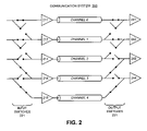
- FIG. 2 illustrates a 4-bit communication system 200 with five communication channels, wherein the input switches 221 are located prior to drivers 211 - 215 in accordance with an embodiment of the present invention.
- Communication system 200 includes drivers 211 - 215 , input switches 221 , output switches 231 , and receivers 241 - 244 .
- output switches 231 selectively couple communication channels 0 - 4 to receivers 241 - 244 .
- communication system 200 is a 4-bit communication system that includes 1 additional bit for refreshing receiver circuits.
- driver 211 is coupled to receiver 241 via communication channel 0
- driver 212 is coupled to receiver 242 via communication channel 1
- driver 214 is coupled to receiver 243 via communication channel 3
- driver 215 is coupled to receiver 244 via communication channel 4 .
- Communication channel 2 is currently inactive, and is undergoing a refresh operation. Note that driver 213 is coupled to inactive communication channel 2 .
- each communication channel has its own driver, and the transmitters for the four bits are selectively coupled to the five drivers 211 - 215 via input switches 221 .
- placing drivers 211 - 215 after input switches 221 facilitates faster drivers with lower power requirements.
- drivers 111 - 114 in communication system 100 must drive the extra parasitic capacitance (or inductance) of input switches 121 , which reduce input switches' 121 effective logical effort and increasing input switches' 121 delay as compared to input switches 221 .
- FIG. 3 illustrates a 4-bit communication system 300 with five communication channels, wherein the receivers are located prior to output switches 331 in accordance with an embodiment of the present invention.
- Communication system 300 includes drivers 311 - 314 , input switches 321 , output switches 331 , and receivers 341 - 345 .
- input switches 321 selectively couple drivers 311 - 314 to communication channels 0 - 4 .
- communication system 300 is a 4-bit communication system that includes 1 additional bit for refreshing receiver circuits.
- driver 311 is coupled to receiver 341 via communication channel 0
- driver 312 is coupled to receiver 342 via communication channel 1
- driver 313 is coupled to receiver 344 via communication channel 3
- driver 314 is coupled to receiver 345 via communication channel 4 .
- Communication channel 2 is currently inactive, and is undergoing a refresh operation. Note that receiver 343 is coupled to inactive communication channel 2 .
- each communication channel has its own receiver, and the receiver logic for the four bits are selectively coupled to the five receivers 341 - 345 via output switches 331 .
- the receiver logic for the four bits are selectively coupled to the five receivers 341 - 345 via output switches 331 .
- FIG. 4 illustrates a 4-bit communication system 400 with five communication channels, wherein the input switches 421 are located prior to drivers 411 - 415 , and wherein the receivers 441 - 445 are located prior to the output switches 431 in accordance with an embodiment of the present invention.
- driver 411 is coupled to receiver 441 via communication channel 0
- driver 412 is coupled to receiver 442 via communication channel 1
- driver 414 is coupled to receiver 444 via communication channel 3
- driver 415 is coupled to receiver 445 via communication channel 4
- Communication channel 2 is currently inactive, and is undergoing a refresh operation. Note that driver 413 and receiver 443 are coupled to inactive communication channel 2 .
- each communication channel has its own driver and receiver.
- the transmitters for the four bits are selectively coupled to the five drivers 411 - 415 via input switches 421 .
- the receiver logic for the four bits are selectively coupled to the five receivers 441 - 445 via output switches 431 .
- placing drivers 411 - 415 after input switches 421 facilitates faster drivers with lower power requirements.
- drivers 111 - 114 in communication system 100 must drive the extra parasitic capacitance (or inductance) of input switches 121 , which reduces input switches' 121 effective logical effort and increases input switches' 121 delay as compared to input switches 421 .
- placing receivers 411 - 415 before output switches 431 keeps output switches 431 from interfering with the data signals, which could be low-swing, for example.
- FIG. 5 illustrates a 4-bit communication system 500 with six communication channels in accordance with an embodiment of the present invention.
- Communication system 500 includes drivers 511 - 514 , input switches 521 , output switches 531 , and receivers 541 - 544 .
- input switches 521 selectively couple drivers 511 - 514 to communication channels 0 - 5
- output switches 531 selectively couple communication channels 0 - 5 to receivers 541 - 544 .
- communication system 500 is a 4-bit communication system that includes 2 additional bits for refreshing receiver circuits.
- driver 511 is coupled to receiver 541 via communication channel 0
- driver 512 is coupled to receiver 542 via communication channel 1
- driver 513 is coupled to receiver 543 via communication channel 4
- driver 514 is coupled to receiver 544 via communication channel 5 .
- Communication channels 2 and 3 are currently inactive, and are undergoing a refresh operation.
- FIG. 6 presents a flowchart illustrating the process of biasing receiver circuits within an integrated circuit in accordance with an embodiment of the present invention.
- the system starts by identifying n receiver circuits within the integrated circuit to be biased (step 602 ).
- the system creates n+m communication channels between n drivers and n receivers, wherein m is a number of additional communication channels, and wherein m>0 (step 604 ).
- the system couples the n+m communication channels to the n drivers, wherein each driver in the n drivers is selectively coupled to m+1 communication channels (step 606 ).
- the system also couples the n+m communication channels to the n receivers, wherein each receiver in the n receivers is selectively coupled to m+1 communication channels (step 608 ). In this way, at any given time n of the communication channels are active and m of the communication channels are inactive.
- the system then refreshes the m inactive communication channels' biases while the m inactive communication channels are not communicating signals (step 610 ). Note that this step is described in more detail in the description of FIGS. 7-9 . Finally, the system periodically reconfigures the switches to selectively couple the drivers and the receivers to the communication channels so that each channel in the n+m communication channels gets refreshed (step 612 ).
- FIG. 7 presents a flowchart illustrating the process of refreshing a communication channel's bias within a single clock cycle in accordance with an embodiment of the present invention.
- the system operates by reconfiguring the switches in a single clock cycle between sample instance times so that timing and voltage margins are maintained for bits being sampled at receivers on the communication channels that are active after the switching (step 702 ).
- FIG. 8 presents a flowchart illustrating the process of refreshing a communication channel's bias over multiple clock cycles in accordance with an embodiment of the present invention.
- the system operates by configuring the communication channel that is being refreshed (C R ) to be operational in parallel with an operating communication channel (C O ) that C R will eventually replace (step 802 ).
- the system then operates C R and C O in parallel until switching effects are minimized (step 804 ). Once any switching effects have settled, the swap can occur. This is a “make-before-break” operation.
- the system switches C R to be the new operating channel and begins refreshing C O (step 806 ).
- FIG. 9 presents a flowchart illustrating the process of sending a refresh signal in accordance with an embodiment of the present invention.
- the system operates by driving a refresh signal to the m communication channels from the transmit side of the communication system (step 902 ).
- one embodiment of the present invention provides a system that facilitates biasing receiver circuits within an integrated circuit.
- Embodiments of the present invention can be implemented in communication systems that use proximity communication.
- one embodiment of the present invention is implemented on a system with capacitively-coupled inputs, while another embodiment of the present invention is implemented on a system with inductively-coupled inputs.
- One embodiment of the present invention allows the receivers to be refreshed periodically without exposing the refresh mechanism to the architecture. As far as any surrounding circuits are concerned, the bits are never taken off-line to be refreshed, and so the existence of a “pause” mechanism is not necessary. In addition, this embodiment eliminates the bandwidth penalty for performing a refresh, because the system always has n channels to provide full-bandwidth communication. Furthermore, this embodiment allows for a slow refresh that can take multiple clock cycles, which allows for small refresh circuits that consume very little power.
Landscapes
- Engineering & Computer Science (AREA)
- Theoretical Computer Science (AREA)
- Physics & Mathematics (AREA)
- General Engineering & Computer Science (AREA)
- General Physics & Mathematics (AREA)
- Electronic Switches (AREA)
Abstract
Description
Claims (24)
Priority Applications (1)
| Application Number | Priority Date | Filing Date | Title |
|---|---|---|---|
| US11/651,222 US7715420B1 (en) | 2006-01-06 | 2007-01-05 | Method and apparatus for refreshing receiver circuits using extra communication bits |
Applications Claiming Priority (2)
| Application Number | Priority Date | Filing Date | Title |
|---|---|---|---|
| US75678006P | 2006-01-06 | 2006-01-06 | |
| US11/651,222 US7715420B1 (en) | 2006-01-06 | 2007-01-05 | Method and apparatus for refreshing receiver circuits using extra communication bits |
Publications (1)
| Publication Number | Publication Date |
|---|---|
| US7715420B1 true US7715420B1 (en) | 2010-05-11 |
Family
ID=42139369
Family Applications (1)
| Application Number | Title | Priority Date | Filing Date |
|---|---|---|---|
| US11/651,222 Active 2028-02-17 US7715420B1 (en) | 2006-01-06 | 2007-01-05 | Method and apparatus for refreshing receiver circuits using extra communication bits |
Country Status (1)
| Country | Link |
|---|---|
| US (1) | US7715420B1 (en) |
Cited By (1)
| Publication number | Priority date | Publication date | Assignee | Title |
|---|---|---|---|---|
| US20100329390A1 (en) * | 2009-06-30 | 2010-12-30 | Sun Microsystems, Inc. | Adaptive offset-compensating decision-feedback receiver |
Citations (15)
| Publication number | Priority date | Publication date | Assignee | Title |
|---|---|---|---|---|
| US5798961A (en) * | 1994-08-23 | 1998-08-25 | Emc Corporation | Non-volatile memory module |
| US5864414A (en) * | 1994-01-26 | 1999-01-26 | British Telecommunications Public Limited Company | WDM network with control wavelength |
| US5912835A (en) * | 1996-06-06 | 1999-06-15 | Nec Corporation | Non-volatile ferroelectric memory device for storing data bits restored upon power-on and intermittently refreshed |
| US5949719A (en) * | 1995-12-20 | 1999-09-07 | International Business Machines Corporation | Field programmable memory array |
| US6301184B1 (en) * | 1999-01-11 | 2001-10-09 | Hitachi, Ltd. | Semiconductor integrated circuit device having an improved operation control for a dynamic memory |
| US6665225B2 (en) * | 2001-12-03 | 2003-12-16 | Mitsubishi Denki Kabushiki Kaisha | Semiconductor integrated circuit with reduction of self refresh current |
| US6686860B2 (en) * | 2000-12-12 | 2004-02-03 | Massachusetts Institute Of Technology | Reconfigurable analog-to-digital converter |
| US6756805B2 (en) * | 1997-08-21 | 2004-06-29 | Micron Technology, Inc. | System for testing integrated circuit devices |
| US6876652B1 (en) * | 2000-05-20 | 2005-04-05 | Ciena Corporation | Network device with a distributed switch fabric timing system |
| US6934749B1 (en) * | 2000-05-20 | 2005-08-23 | Ciena Corporation | Tracking distributed data retrieval in a network device |
| US7002397B2 (en) * | 1999-01-26 | 2006-02-21 | Renesas Technology Corp. | Method of setting back bias of MOS circuit, and MOS integrated circuit |
| US7046562B2 (en) * | 2002-05-29 | 2006-05-16 | Micron Technology, Inc. | Integrated circuit reset circuitry |
| US20060193248A1 (en) * | 2005-02-28 | 2006-08-31 | Clarence Filsfils | Loop prevention technique for MPLS using service labels |
| US7359322B2 (en) * | 2002-08-12 | 2008-04-15 | Telcordia Technologies, Inc. | Dynamic bandwidth reallocation |
| US7483411B2 (en) * | 2001-06-04 | 2009-01-27 | Nec Corporation | Apparatus for public access mobility LAN and method of operation thereof |
-
2007
- 2007-01-05 US US11/651,222 patent/US7715420B1/en active Active
Patent Citations (15)
| Publication number | Priority date | Publication date | Assignee | Title |
|---|---|---|---|---|
| US5864414A (en) * | 1994-01-26 | 1999-01-26 | British Telecommunications Public Limited Company | WDM network with control wavelength |
| US5798961A (en) * | 1994-08-23 | 1998-08-25 | Emc Corporation | Non-volatile memory module |
| US5949719A (en) * | 1995-12-20 | 1999-09-07 | International Business Machines Corporation | Field programmable memory array |
| US5912835A (en) * | 1996-06-06 | 1999-06-15 | Nec Corporation | Non-volatile ferroelectric memory device for storing data bits restored upon power-on and intermittently refreshed |
| US6756805B2 (en) * | 1997-08-21 | 2004-06-29 | Micron Technology, Inc. | System for testing integrated circuit devices |
| US6301184B1 (en) * | 1999-01-11 | 2001-10-09 | Hitachi, Ltd. | Semiconductor integrated circuit device having an improved operation control for a dynamic memory |
| US7002397B2 (en) * | 1999-01-26 | 2006-02-21 | Renesas Technology Corp. | Method of setting back bias of MOS circuit, and MOS integrated circuit |
| US6934749B1 (en) * | 2000-05-20 | 2005-08-23 | Ciena Corporation | Tracking distributed data retrieval in a network device |
| US6876652B1 (en) * | 2000-05-20 | 2005-04-05 | Ciena Corporation | Network device with a distributed switch fabric timing system |
| US6686860B2 (en) * | 2000-12-12 | 2004-02-03 | Massachusetts Institute Of Technology | Reconfigurable analog-to-digital converter |
| US7483411B2 (en) * | 2001-06-04 | 2009-01-27 | Nec Corporation | Apparatus for public access mobility LAN and method of operation thereof |
| US6665225B2 (en) * | 2001-12-03 | 2003-12-16 | Mitsubishi Denki Kabushiki Kaisha | Semiconductor integrated circuit with reduction of self refresh current |
| US7046562B2 (en) * | 2002-05-29 | 2006-05-16 | Micron Technology, Inc. | Integrated circuit reset circuitry |
| US7359322B2 (en) * | 2002-08-12 | 2008-04-15 | Telcordia Technologies, Inc. | Dynamic bandwidth reallocation |
| US20060193248A1 (en) * | 2005-02-28 | 2006-08-31 | Clarence Filsfils | Loop prevention technique for MPLS using service labels |
Cited By (2)
| Publication number | Priority date | Publication date | Assignee | Title |
|---|---|---|---|---|
| US20100329390A1 (en) * | 2009-06-30 | 2010-12-30 | Sun Microsystems, Inc. | Adaptive offset-compensating decision-feedback receiver |
| US8798530B2 (en) * | 2009-06-30 | 2014-08-05 | Oracle America, Inc. | Adaptive offset-compensating decision-feedback receiver |
Similar Documents
| Publication | Publication Date | Title |
|---|---|---|
| TWI760136B (en) | Apparatuses and methods for power efficient driver circuits | |
| US6094375A (en) | Integrated circuit memory devices having multiple data rate mode capability and methods of operating same | |
| US20110307672A1 (en) | Memory interface with interleaved control information | |
| CN109285581B (en) | Memory device including a plurality of power rails and method of operating the same | |
| US7345945B2 (en) | Line driver circuit for a semiconductor memory device | |
| KR100680520B1 (en) | Multi-port memory cell with preset | |
| US6594194B2 (en) | Memory array with common word line | |
| US5506522A (en) | Data input/output line sensing circuit of a semiconductor integrated circuit | |
| US11119959B2 (en) | Data communication and processing method of master device and slave device | |
| JP2007535198A (en) | Flash / dynamic random access memory field programmable gate array | |
| US7715420B1 (en) | Method and apparatus for refreshing receiver circuits using extra communication bits | |
| US7768865B2 (en) | Address decoder and/or access line driver and method for memory devices | |
| US7573290B2 (en) | Data output driver for reducing noise | |
| KR100298522B1 (en) | Method and apparatus for single clocked, non-overlapping access in a multi-port memory cell | |
| US9406364B2 (en) | Codec to reduce simultaneously switching outputs | |
| US7551514B2 (en) | Semiconductor memory utilizing a method of coding data | |
| US7800936B2 (en) | Latch-based random access memory | |
| US11093434B2 (en) | Communication system and operation method | |
| US10997097B2 (en) | Enabling high speed command address interface for random read | |
| CN115698972A (en) | Method for performing system and power management through serial data communication interface | |
| KR100244247B1 (en) | Sensing circuit | |
| US20150039843A1 (en) | Circuits and methods for providing data to and from arrays of memory cells | |
| US7085178B1 (en) | Low-power memory write circuits | |
| US5917769A (en) | Method and system rotating data in a memory array device | |
| KR100378855B1 (en) | Method and circuit for multistage readout operation |
Legal Events
| Date | Code | Title | Description |
|---|---|---|---|
| AS | Assignment |
Owner name: SUN MICROSYSTEMS, INC.,CALIFORNIA Free format text: ASSIGNMENT OF ASSIGNORS INTEREST;ASSIGNORS:HO, RONALD;DROST, ROBERT J.;REEL/FRAME:019020/0507 Effective date: 20070227 |
|
| FEPP | Fee payment procedure |
Free format text: PAYOR NUMBER ASSIGNED (ORIGINAL EVENT CODE: ASPN); ENTITY STATUS OF PATENT OWNER: LARGE ENTITY |
|
| STCF | Information on status: patent grant |
Free format text: PATENTED CASE |
|
| FPAY | Fee payment |
Year of fee payment: 4 |
|
| AS | Assignment |
Owner name: ORACLE AMERICA, INC., CALIFORNIA Free format text: MERGER AND CHANGE OF NAME;ASSIGNORS:ORACLE USA, INC.;SUN MICROSYSTEMS, INC.;ORACLE AMERICA, INC.;REEL/FRAME:037306/0292 Effective date: 20100212 |
|
| MAFP | Maintenance fee payment |
Free format text: PAYMENT OF MAINTENANCE FEE, 8TH YEAR, LARGE ENTITY (ORIGINAL EVENT CODE: M1552) Year of fee payment: 8 |
|
| MAFP | Maintenance fee payment |
Free format text: PAYMENT OF MAINTENANCE FEE, 12TH YEAR, LARGE ENTITY (ORIGINAL EVENT CODE: M1553); ENTITY STATUS OF PATENT OWNER: LARGE ENTITY Year of fee payment: 12 |