US7703992B2 - Single piece diplexer and triplexer housing - Google Patents
Single piece diplexer and triplexer housing Download PDFInfo
- Publication number
- US7703992B2 US7703992B2 US12/028,519 US2851908A US7703992B2 US 7703992 B2 US7703992 B2 US 7703992B2 US 2851908 A US2851908 A US 2851908A US 7703992 B2 US7703992 B2 US 7703992B2
- Authority
- US
- United States
- Prior art keywords
- receptacle
- diameter
- optical
- receive
- housing
- Prior art date
- Legal status (The legal status is an assumption and is not a legal conclusion. Google has not performed a legal analysis and makes no representation as to the accuracy of the status listed.)
- Active
Links
Images


Classifications
-
- G—PHYSICS
- G02—OPTICS
- G02B—OPTICAL ELEMENTS, SYSTEMS OR APPARATUS
- G02B6/00—Light guides; Structural details of arrangements comprising light guides and other optical elements, e.g. couplings
- G02B6/24—Coupling light guides
- G02B6/42—Coupling light guides with opto-electronic elements
- G02B6/4292—Coupling light guides with opto-electronic elements the light guide being disconnectable from the opto-electronic element, e.g. mutually self aligning arrangements
-
- G—PHYSICS
- G02—OPTICS
- G02B—OPTICAL ELEMENTS, SYSTEMS OR APPARATUS
- G02B6/00—Light guides; Structural details of arrangements comprising light guides and other optical elements, e.g. couplings
- G02B6/24—Coupling light guides
- G02B6/42—Coupling light guides with opto-electronic elements
- G02B6/4201—Packages, e.g. shape, construction, internal or external details
- G02B6/4204—Packages, e.g. shape, construction, internal or external details the coupling comprising intermediate optical elements, e.g. lenses, holograms
- G02B6/4206—Optical features
-
- G—PHYSICS
- G02—OPTICS
- G02B—OPTICAL ELEMENTS, SYSTEMS OR APPARATUS
- G02B6/00—Light guides; Structural details of arrangements comprising light guides and other optical elements, e.g. couplings
- G02B6/24—Coupling light guides
- G02B6/42—Coupling light guides with opto-electronic elements
- G02B6/4201—Packages, e.g. shape, construction, internal or external details
- G02B6/4246—Bidirectionally operating package structures
Definitions
- bidirectional and triple-bidirectional data transmission is often required, which in turn requires multiple elements to be packaged and aligned in an optoelectronic module.
- modules that include multiple elements are a bidirectional module, also known as a diplexer, and triple bidirectional module, also known a triplexer.
- a common approach to manufacturing both diplexers and triplexer modules is to create a housing that is implemented as two or more pieces. The two or more pieces are then fit together using known fabrication processes. Often, however, this multiple piece approach requires two or more fabrication operations to achieve the necessary accuracy and/or function of all the features. Accordingly, the multiple piece approach is expensive and time consuming.
- An embodiment disclosed herein relates to single piece optoelectronic module housing.
- the housing comprises a first receptacle configured to receive a first optical assembly, a second receptacle configured to receive a second optical assembly, a third receptacle configured to receive an optical fiber, and at least one angled surface configured to have a filter placed thereon.
- At least one compliant press fit feature is implemented as part of one of the receptacles.
- the optoelectronic module housing is a single piece housing configured such that the receptacles and angled surface are integral parts of the single piece housing.
- An additional embodiment disclosed herein relates to single piece optoelectronic module housing.
- the housing comprises a first receptacle configured to receive a first optical assembly, a second receptacle configured to receive a second optical assembly, a third receptacle configured to receive a third optical assembly, and a fourth receptacle configured to receive an optical fiber.
- the housing also comprises a first angled pocket receptacle configured to have one or more optical elements placed therein and a second angled pocket receptacle configured to have one or more optical elements placed therein.
- the optoelectronic module housing is a single piece housing configured such that the receptacles and angled pocket receptacles are integral parts of the single piece housing.
- a further embodiment disclosed herein relates to single piece optoelectronic module housing.
- the housing comprises a first receptacle configured to receive a first optical assembly, a second receptacle configured to receive a second optical assembly, a third receptacle configured to receive a third optical assembly, and a fourth receptacle configured to receive an optical fiber.
- the housing also comprises a first angled pocket receptacle configured to have one or more optical elements placed therein, a second angled pocket receptacle configured to have one or more optical elements placed therein, and at least one compliant press fit feature implemented as part of one of the receptacles.
- the optoelectronic module housing is a single piece housing configured such that the receptacles and angled pocket receptacles are integral parts of the single piece housing.
- FIGS. 1A-1D illustrate an embodiment of a single piece diplexer housing in accordance with the principles of the present invention
- FIGS. 2A-2D illustrate an embodiment of a single piece triplexer housing in accordance with the principles of the present invention
- FIGS. 3A-3E illustrate an alternative embodiment of a single piece triplexer housing in accordance with the principles of the present invention.
- FIGS. 4A-4B illustrate an embodiment of a single piece triplexer housing that implements multiple angled pocket receptacles in accordance with the principles of the present invention.
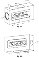
- FIGS. 1A-1D illustrate different views of one embodiment of a one piece diplexer housing in accordance with the principles of the present invention, designated generally at 100 .
- FIGS. 1A-1D illustrate different views of one embodiment of a one piece diplexer housing in accordance with the principles of the present invention, designated generally at 100 .
- FIGS. 1A-1D illustrate different views of one embodiment of a one piece diplexer housing in accordance with the principles of the present invention, designated generally at 100 . Note that the embodiment of FIGS. 1A-1D is only one of numerous embodiments in which the principles of the present invention may be practiced and should not be used to limit the scope of the appended claims.
- Diplexer 100 is implemented as a one piece housing, which may be manufactured using Metal Injection Molding (MIM) processes as will be described in further detail to follow.
- diplexer 100 may be made from metal. Examples of metals that may be used include, but are not limited to, carbon steel, and 416 steel. Other suitable materials known in the art may also be used to make triplexer diplexer 100 . Since only one piece is used as a housing, additional required alignment and attachment steps of multiple piece housings are reduced to a minimum, resulting in higher reliability and lower assembly cost when compared to multiple piece housings.
- MIM Metal Injection Molding
- diplexer 100 includes a first receptacle 110 that is configured to hold an optical device such as an optical transmitter assembly 150 .
- first receptacle 110 has two stepped diameters.
- a first portion 112 has a diameter D 1 .
- diameter D 1 is sized large enough to receive a laser header 152 .
- Receptacle 110 also includes a second portion 114 that has a diameter D 2 that is typically smaller than diameter D 1 . As illustrated, the change or step between the diameters of portions 112 and 114 creates a step 113 inside of receptacle 110 . As is illustrated in FIG. 1D , diameter D 2 is sized large enough to receive a laser can 154 .
- a third portion 116 of receptacle 110 has a diameter D 3 that is typically smaller than diameter D 2 . As illustrated, the change or step between the diameters of portions 114 and 116 creates a step 117 inside of receptacle 110 . As is illustrated in FIG. 1D , diameter D 3 is sized large enough to receive an optical isolator 156 , which may or may not be part of laser assembly 150 .
- diplexer 100 includes a second receptacle 120 that is configured to hold an optical assembly such as a photodiode assembly 160 .
- second receptacle 120 has two stepped diameters.
- a first portion 122 has a diameter D 6 .
- diameter D 6 is sized large enough to receive a photodiode header 162 .
- Receptacle 120 also includes a second portion 124 that has a diameter D 7 that is typically smaller than diameter D 6 . As illustrated, the change or step between the diameters of portions 122 and 124 creates a step 123 inside of receptacle 120 . As is illustrated in FIG. 1D , diameter D 7 is sized large enough to receive a nose portion of assembly 160 .
- a third portion 126 of receptacle 120 has a diameter D 8 that is typically smaller than diameter D 7 . As illustrated, the change or step between the diameters of portions 124 and 126 creates a step 125 inside of receptacle 120 . As is illustrated in FIG. 1D , diameter D 8 is sized large enough to receive a photodiode lens 164 .
- Diplexer 100 also includes a third receptacle 130 that is configured to receive an optical fiber such as fiber 170 .
- Receptacle 130 has a diameter D 5 that is sized large enough to receive the fiber.
- diplexer 100 further includes a pocket 140 for selective filter alignment.
- Pocket 140 has angled surfaces 142 and 144 , with angled surface 142 being where the selective filter, such as filter 190 of FIG. 1D , may be placed inside single piece diplexer 100 .
- Angled surface 142 allows for convenient positioning of filter 190 before it is attached permanently to the surface with epoxy, which results in faster and more accurate attachment.
- Angled surfaces 142 and 144 are configured to reduce cross talk and/or back reflection between optical signals during operation of diplexer 100 .
- pocket 140 is a through pocket that allows an optical signal to be transmitted between an optical assembly residing in first receptacle 110 and the fiber residing in third receptacle 130 and allows an optical signal to be transmitted between an optical assembly residing in second receptacle 120 and the fiber residing in third receptacle 130 .
- pocket 140 is an integral part of diplexer 100 , thus removing the need for separate parts to house filter 190 .
- transmit assembly 150 may be placed in first receptacle 110
- photodiode assembly 160 may be placed in second receptacle 120
- fiber 170 may be placed in third receptacle 130 .
- the placement of the various components in a specific receptacle is for illustration only and is not to be used to limit the scope of the appended claims.
- One of skill in the art will appreciate that the various components may be placed in other receptacles as circumstances warrant.
- first receptacle 110 includes compliant press fit features 115 .
- the compliant press fit features are in the form of slots, although in other embodiments, compliant press fit features 115 may also be, but are not limited to, crush ribs or teeth. Note that the slots may have various shapes as they may also be angled or tapered.
- Compliant press fit features 115 allow for transmit assembly 150 to be press fit or interference fit into first receptacle 110 .
- the use of compliant press fit features 115 advantageously allow for diplexer 100 to be manufactured as one piece using the inexpensive MIM process. Note that although FIG. 1A only shows receptacle 110 as including compliant press fit features 115 , the other receptacles may also include compliant press fit features 115 as circumstances warrant.
- FIGS. 2A-2D illustrate different views of one embodiment of a one piece triplexer housing in accordance with the principles of the present invention, designated generally at 200 .
- FIGS. 2A-2D illustrate different views of one embodiment of a one piece triplexer housing in accordance with the principles of the present invention, designated generally at 200 .
- FIGS. 2A-2D illustrate different views of one embodiment of a one piece triplexer housing in accordance with the principles of the present invention, designated generally at 200 . Note that the embodiment of FIGS. 2A-2D is only one of numerous embodiments in which the principles of the present invention may be practiced and should not be used to limit the scope of the appended claims.
- Triplexer 200 may be manufactured using the MIM process.
- triplexer 200 may be made from metal. Examples of metals that may be used include, but are not limited to, carbon steel, and 416 steel. Other suitable materials known in the art may also be used to make triplexer 200 . Since only one piece is used as a housing, additional required alignment and attachment steps of multiple piece housings are reduced to a minimum, resulting in higher reliability and lower assembly cost when compared to multiple piece housings.
- triplexer 200 includes a first receptacle 210 that is configured to hold an optical device such as an optical transmitter assembly 270 .
- first receptacle 210 has a diameter D 1 .
- diameter D 1 is sized large enough to receive the portions of assembly 270 , namely laser header 271 , laser can 272 , and laser lens 273 .
- triplexer 200 includes a second receptacle 220 that is configured to hold an optical assembly such as a photodiode assembly 285 .
- second receptacle 220 has two stepped diameters.
- a first portion 222 has a diameter D 2 .
- diameter D 2 is sized large enough to receive a photodiode header 286 .
- Receptacle 220 also includes a second portion 224 that has a diameter D 3 that is typically smaller than diameter D 2 . As illustrated, the change or step between the diameters of portions 222 and 224 creates a step 221 inside of receptacle 220 . As is illustrated in FIG. 2D , diameter D 3 is sized large enough to receive a photodiode lens 281 .
- a third portion 226 of receptacle 220 has a diameter D 4 that is typically smaller than diameter D 3 .
- the change or step between the diameters of portions 224 and 226 creates a step 223 inside of receptacle 220 .
- diameter D 4 is sized large enough to receive a portion of photodiode lens 287 and also to receive a blocking filter 288 .
- the surface 225 where blocking filter 288 is placed is angled to reduce back refection into the photodiode assembly.
- triplexer 200 includes a third receptacle 230 that is configured to hold an optical assembly such as a photodiode assembly 280 .
- third receptacle 230 has two stepped diameters.
- a first portion 232 has a diameter D 5 .
- diameter D 5 is sized large enough to receive a photodiode header 281 .
- Receptacle 230 also includes a second portion 234 that has a diameter D 6 that is typically smaller than diameter D 5 . As illustrated, the change or step between the diameters of portions 232 and 234 creates a step 231 inside of receptacle 230 . As is illustrated in FIG. 2D , diameter D 5 is sized large enough to receive a photodiode lens 282 .
- a third portion 236 of receptacle 230 has a diameter D 7 that is typically smaller than diameter D 6 .
- the change or step between the diameters of portions 234 and 236 creates a step 233 inside of receptacle 230 .
- diameter D 7 is sized large enough to receive a portion of photodiode lens 282 and also to receive a blocking filter 283 .
- the surface 235 where blocking filter 283 is placed is angled to reduce back refection into the photodiode assembly.
- Triplexer 200 also includes a fourth receptacle 240 that is configured to receive an optical fiber such as fiber 290 .
- Receptacle 240 has a diameter D 8 that is sized large enough to receive the fiber 290 and a fiber lens 291 .
- triplexer 200 includes a rectangular through hole 250 , which advantageously may be manufactured using the MIM process. Rectangular through hole 250 allows an optical signal to be transmitted between optical assemblies residing in first, second and third receptacles 210 , 220 , and 230 and a fiber residing in fourth receptacle 240 .
- Angled surfaces 260 and 265 are configured to hold selective filters 295 and 296 respectively. Angled surfaces 260 and 265 allow for convenient positioning of filters 295 and 296 before they are attached permanently to the surface with epoxy, which results in faster and more accurate attachment. Angled surfaces 260 , 265 , 266 , and 267 are designed to reduce cross talk and/or back reflection between optical signals during operation of triplexer 200 .
- rectangular through hole 250 and angled surfaces 260 , 265 , 266 , and 267 are an integral part of triplexer 200 , thus removing the need for separate parts to house filters 295 and 296 .
- transmit assembly 270 may be placed in first receptacle 210
- photodiode assembly 285 may be placed in second receptacle 220
- photodiode assembly 280 may be placed in third receptacle 230
- fiber 290 may be placed in fourth receptacle 240 .
- the placement of the various components in a specific receptacle is for illustration only and is not to be used to limit the scope of the appended claims.
- the various components may be placed in other receptacles as circumstances warrant.
- fourth receptacle 240 includes compliant press fit features 245 .
- the compliant press fit features are in the form of teeth, although in other embodiments, compliant press fit features 245 may also be, but are not limited to, crush ribs or slot such as those described in relation to FIG. 1A above.
- Compliant press fit features 245 allow for the fiber 290 or lens 291 to be press fit or interference fit into fourth receptacle 240 .
- the use of compliant press fit features 245 advantageously allow for triplexer 200 to be manufactured as one piece using the inexpensive MIM process. Note that although FIG. 2A only shows receptacle 240 as including compliant press fit features 245 , the other receptacles may also include compliant press fit features 245 as circumstances warrant.
- FIGS. 3A-3E illustrate different views of an alternative embodiment of a one piece triplexer housing in accordance with the principles of the present invention, designated generally at 300 .
- FIGS. 3A-3E illustrate different views of an alternative embodiment of a one piece triplexer housing in accordance with the principles of the present invention, designated generally at 300 .
- FIGS. 3A-3E illustrate different views of an alternative embodiment of a one piece triplexer housing in accordance with the principles of the present invention, designated generally at 300 . Note that the embodiment of FIGS. 3A-3E is only one of numerous embodiments in which the principles of the present invention may be practiced and should not be used to limit the scope of the appended claims.
- Triplexer 300 is implemented as a one piece housing, which may be manufactured using the MIM process or may be manufactured using traditional machining processes.
- triplexer 300 may be made from metal. Examples of metals that may be used include, but are not limited to, carbon steel, and 416 steel. Other suitable materials known in the art may also be used to make triplexer 300 Since only one piece is used as a housing, additional required alignment and attachment steps of multiple piece housings are reduced to a minimum, resulting in higher reliability and lower assembly cost when compared to multiple piece housings.
- triplexer 300 includes a first receptacle 310 that is configured to hold an optical device such as an optical transmitter assembly 370 .
- first receptacle 310 has a diameter D 1 .
- diameter D 1 is sized large enough to receive the portions assembly 271 , namely laser header 271 , laser can 272 , and laser lens 273 .
- triplexer 300 includes a second receptacle 320 that is configured to hold an optical assembly such as a photodiode assembly 380 .
- second receptacle 320 has a stepped diameter.
- a first portion 322 has a diameter D 2 .
- diameter D 2 is sized large enough to receive a photodiode header 381 .
- Receptacle 320 also includes a second portion 324 that has a diameter D 3 that is typically smaller than diameter D 2 . As illustrated, the change or step between the diameters of portions 322 and 324 creates a step 321 inside of receptacle 320 . As is illustrated in FIG. 2D , diameter D 3 is sized large enough to receive a photodiode lens 382 .
- triplexer 300 includes a third receptacle 330 that is configured to hold an optical assembly such as a photodiode assembly 385 .
- third receptacle 330 has a stepped diameter.
- a first portion 332 has a diameter D 5 .
- diameter D 5 is sized large enough to receive a photodiode header 385 .
- Receptacle 330 also includes a second portion 334 that has a diameter D 6 that is typically smaller than diameter D 5 . As illustrated, the change or step between the diameters of portions 332 and 334 creates a step 331 inside of receptacle 330 . As is illustrated in FIG. 3D , diameter D 5 is sized large enough to receive a photodiode lens 387 .
- Triplexer 300 also includes a fourth receptacle 340 that is configured to receive an optical fiber such as fiber 390 .
- Receptacle 340 has a diameter D 4 that is sized large enough to receive the fiber 390 and a fiber lens 391 .
- triplexer 300 includes angled pocket receptacles 350 and 360 , which may be manufactured by a side cut using wire cutting, mill cuts, or other known methods into one piece triplexer 300 .
- the angled pocket receptacles 350 and 360 are triangular in shape in FIGS. 3A-3E . It will be appreciated, however, that angled pocket receptacles 350 and 360 may be various shapes and sizes as circumstances warrant. For example, in some embodiments angled pocket receptacles 350 and 360 may be shapes other than triangles. It should also be noted that in some embodiments, angled pocket receptacles 350 and 360 are manufactured to go through the entire thickness of one piece triplexer 300 .
- Angled pocket receptacles 350 and 360 include angled surfaces 352 , 354 , 356 and 362 , 364 , 366 respectively.
- Surfaces 352 and 362 are configured to hold selective filters 395 and 398 respectively.
- Surfaces 354 and 364 are configured hold blocking filters 397 and 399 respectively.
- Surfaces 356 and 366 are configured to hold additional filters as circumstances warrant, such as a filter 396 .
- angled surfaces 352 , 354 , 356 and 362 , 364 , 366 allow for convenient positioning of the various filters before they are attached permanently to the surface with epoxy, which results in faster and more accurate attachment.
- a cover (not shown) may be placed over angled pockets 350 and 360 .
- Angled surfaces 352 , 354 , 356 and 362 , 364 , 366 are designed to reduce cross talk and/or back reflection between optical signals during operation of triplexer 300 .
- the angled surfaces 352 , 354 , 356 and 362 , 364 , 366 are an integral part of one piece triplexer 300 , thus removing the need for separate parts to house the various filters.
- angled surfaces 352 , 354 , 356 and 362 , 364 , 366 may be implemented with various angles as circumstances warrant to help maximize the cross talk and back reflection reduction.
- surfaces 352 and 362 may be implemented in the 40 degrees to 50 degrees range
- surfaces 354 and 364 may be implemented in the 0 degrees to 10 degrees range
- surfaces 356 and 366 may be implemented in the 80 degrees to 90 degrees range.
- transmit assembly 370 may be placed in first receptacle 310
- photodiode assembly 380 may be placed in second receptacle 320
- photodiode assembly 385 may be placed in third receptacle 330
- fiber 390 may be placed in fourth receptacle 340 .
- the placement of the various components in a specific receptacle is for illustration only and is not to be used to limit the scope of the appended claims.
- the various components may be placed in other receptacles as circumstances warrant.
- first receptacle 310 includes a compliant press fit feature 315 , which is in the form of slots such as those previously described.
- fourth receptacle 340 includes compliant press fit features 345 , which is in the form of teeth such as those previously described.
- compliant press fit features 315 and 345 may also be, but are not limited to, teeth, crush ribs or slots such as those described above.
- Compliant press fit features 315 and 345 allow for an optical assembly and/or fiber to be press fit or interference fit into first receptacle 315 and/or fourth receptacle 340 .
- compliant press fit features 315 and 345 advantageously allow for triplexer 300 to be manufactured as one piece using the inexpensive MIM process. Note that although FIG. 3E only shows receptacles 310 and 340 as including compliant press fit features 315 and 345 , the other receptacles may also include compliant press fit features 315 and 345 as circumstances warrant.
- one piece triplexer housing 300 also includes cuts 305 and 306 .
- Cuts 305 and 306 may be manufactured using various machining techniques known in the art and are integral to the triplexer housing. Although illustrated as being round, cuts 305 and 306 may be other shapes such as angled slots as circumstances warrant.
- cuts 305 and 306 help to reduce cross talk between the optical assemblies of triplexer 300 . This is illustrated further in FIG. 3D by the arrows in cut 305 , which show how cut 305 helps to suppress cross talk between optical assembly 370 and optical assembly 380 .
- FIGS. 4A and 4B illustrate an embodiment of a triplexer 400 that includes multiple angled pocket receptacles.
- this embodiment includes a first receptacle 410 that is typically configured to receive an optical assembly such as a laser header.
- Triplexer 400 also includes second, third, fourth, and fifth receptacles 420 , 430 , 440 , and 450 that are typically configured to receive optical assemblies such as photodiode headers.
- a sixth receptacle 460 is configured to receive a fiber.
- Receptacles 410 - 460 are similar to like receptacles previously described and so need not be described in further detail. Further, compliant press fit features may be included as circumstances warrant as previously described.
- triplexer 400 includes multiple angled pocket receptacles 480 , 485 , 490 , and 495 . These angled pocket receptacles are configured to hold various filters as previously described in relation to angled pocket receptacles 350 and 360 .
- the use of multiple angled pocket receptacles in a one piece triplexer housing is partially enabled by an optical design that implements a collimated (or slightly convergent) beam as described in commonly assigned, co-pending U.S. Provisional Application Ser. No. 60/889,912, filed Feb. 14, 2007, which is incorporated herein by reference in its entirety.
- FIGS. 4A-4B show four angled pocket receptacles, this is for illustration only. The principles of the present invention allow for more than four angled pocket receptacles to be implemented as circumstances warrant.
Abstract
Description
Claims (7)
Priority Applications (1)
| Application Number | Priority Date | Filing Date | Title |
|---|---|---|---|
| US12/028,519 US7703992B2 (en) | 2007-02-08 | 2008-02-08 | Single piece diplexer and triplexer housing |
Applications Claiming Priority (3)
| Application Number | Priority Date | Filing Date | Title |
|---|---|---|---|
| US90026307P | 2007-02-08 | 2007-02-08 | |
| US96119007P | 2007-07-17 | 2007-07-17 | |
| US12/028,519 US7703992B2 (en) | 2007-02-08 | 2008-02-08 | Single piece diplexer and triplexer housing |
Publications (2)
| Publication Number | Publication Date |
|---|---|
| US20080193088A1 US20080193088A1 (en) | 2008-08-14 |
| US7703992B2 true US7703992B2 (en) | 2010-04-27 |
Family
ID=39682135
Family Applications (1)
| Application Number | Title | Priority Date | Filing Date |
|---|---|---|---|
| US12/028,519 Active US7703992B2 (en) | 2007-02-08 | 2008-02-08 | Single piece diplexer and triplexer housing |
Country Status (4)
| Country | Link |
|---|---|
| US (1) | US7703992B2 (en) |
| EP (1) | EP2115511B1 (en) |
| CN (1) | CN101669055B (en) |
| WO (1) | WO2008098214A1 (en) |
Cited By (5)
| Publication number | Priority date | Publication date | Assignee | Title |
|---|---|---|---|---|
| US20130004132A1 (en) * | 2011-06-29 | 2013-01-03 | Chien-Hsiung Chiu | Bi-Directional Fiber Optic Transceivers, Housings Therefor, and Methods for Making and Using the Same |
| WO2018044993A1 (en) * | 2016-08-31 | 2018-03-08 | Applied Optoelectronics, Inc. | An optical component assembly with a vertical mounting structure for multi-angle light path alignment and an optical subassembly using the same |
| US10044445B2 (en) | 2016-08-31 | 2018-08-07 | Applied Optoelectronics, Inc. | Techniques for reducing electrical interconnection losses between a transmitter optical subassembly (TOSA) and associated driver circuitry and an optical transceiver system using the same |
| US10921535B1 (en) * | 2019-12-01 | 2021-02-16 | Ezconn Corporation | Optical sub-assembly and telescopic-shaped core cylinder module thereof |
| US11409062B2 (en) * | 2019-03-18 | 2022-08-09 | Usenlight Corporation | Optical transceiver module and optical cable module |
Families Citing this family (7)
| Publication number | Priority date | Publication date | Assignee | Title |
|---|---|---|---|---|
| KR101256379B1 (en) * | 2009-06-01 | 2013-04-25 | 미쓰비시덴키 가부시키가이샤 | Light transmission/reception module |
| US9213156B2 (en) * | 2011-08-17 | 2015-12-15 | Source Photonics, Inc. | Optical receiver with reduced cavity size and methods of making and using the same |
| CN102523043B (en) * | 2011-12-15 | 2014-08-20 | 深圳市易飞扬通信技术有限公司 | Photodetector |
| CN102854584A (en) * | 2012-10-09 | 2013-01-02 | 索尔思光电(成都)有限公司 | Single-fiber two-way optical transceiver |
| EP3146298B1 (en) | 2014-05-21 | 2019-03-06 | Datalogic IP TECH S.r.l. | Method to realize an optical module |
| US9684141B1 (en) * | 2016-04-25 | 2017-06-20 | Applied Optoelectronics, Inc. | Techniques for reducing ingress of foreign matter into an optical subassembly |
| TW202109104A (en) * | 2019-01-18 | 2021-03-01 | 美商山姆科技公司 | Sealed optical transceiver |
Citations (10)
| Publication number | Priority date | Publication date | Assignee | Title |
|---|---|---|---|---|
| JPS63225220A (en) | 1987-03-16 | 1988-09-20 | Kawasaki Heavy Ind Ltd | Color image projector |
| US4904043A (en) | 1988-06-15 | 1990-02-27 | American Telephone And Telegraph Company, At&T Bell Laboratories | Optical data link dual wavelength coupler |
| JPH05215935A (en) | 1992-02-06 | 1993-08-27 | Nec Corp | Optical multiplexing and demultiplexing device and optical multiplexer |
| US6040934A (en) * | 1996-06-21 | 2000-03-21 | Kabushiki Kaisha Toshiba | Receptacle-type optical transmission/reception apparatus |
| US20020028049A1 (en) * | 2000-09-05 | 2002-03-07 | Meir Bartur | Optical networking unit employing optimized optical packaging |
| US20030147601A1 (en) * | 2002-02-01 | 2003-08-07 | Meir Bartur | Hybrid optical module employing integration of electronic circuitry with active optical devices |
| US6749347B1 (en) * | 2000-03-30 | 2004-06-15 | Fujitsu Limited | Laser diode module and assembling method therefor |
| KR20060023916A (en) | 2004-09-11 | 2006-03-15 | (주) 빛과 전자 | Integrated triplexer optical sub-assembly |
| KR20060102783A (en) | 2005-03-25 | 2006-09-28 | (주) 빛과 전자 | Integrated optical sub-assembly |
| US20080175591A1 (en) * | 2007-01-19 | 2008-07-24 | Juhyun Yu | Filter assembly and optical module using same |
Family Cites Families (9)
| Publication number | Priority date | Publication date | Assignee | Title |
|---|---|---|---|---|
| JPH065331B2 (en) * | 1987-03-16 | 1994-01-19 | 沖電気工業株式会社 | Hybrid multiplexer / demultiplexer |
| JP3739540B2 (en) * | 1997-08-04 | 2006-01-25 | アルプス電気株式会社 | Optical transceiver module |
| US6571033B2 (en) * | 2001-09-28 | 2003-05-27 | Corning Incorporated | Optical signal device |
| JP2005134803A (en) * | 2003-10-31 | 2005-05-26 | Tdk Corp | Ferrule with optical isolator and optical transmission/reception module equipped with the same |
| US7322754B2 (en) * | 2004-02-11 | 2008-01-29 | Jds Uniphase Corporation | Compact optical sub-assembly |
| KR100566256B1 (en) | 2004-02-13 | 2006-03-29 | 삼성전자주식회사 | Bi-directional optical transceiver module |
| US20060133742A1 (en) * | 2004-12-17 | 2006-06-22 | Ruegg Eugen H | Universal multi-port optical block assembly with configurable optical port |
| KR100640421B1 (en) * | 2004-12-28 | 2006-10-31 | 삼성전자주식회사 | Optical module for multi-wavelength |
| JP4428274B2 (en) * | 2005-04-04 | 2010-03-10 | 住友電気工業株式会社 | Bidirectional optical module |
-
2008
- 2008-02-08 EP EP08743445.2A patent/EP2115511B1/en not_active Not-in-force
- 2008-02-08 US US12/028,519 patent/US7703992B2/en active Active
- 2008-02-08 CN CN200880010383.3A patent/CN101669055B/en not_active Expired - Fee Related
- 2008-02-08 WO PCT/US2008/053491 patent/WO2008098214A1/en active Application Filing
Patent Citations (10)
| Publication number | Priority date | Publication date | Assignee | Title |
|---|---|---|---|---|
| JPS63225220A (en) | 1987-03-16 | 1988-09-20 | Kawasaki Heavy Ind Ltd | Color image projector |
| US4904043A (en) | 1988-06-15 | 1990-02-27 | American Telephone And Telegraph Company, At&T Bell Laboratories | Optical data link dual wavelength coupler |
| JPH05215935A (en) | 1992-02-06 | 1993-08-27 | Nec Corp | Optical multiplexing and demultiplexing device and optical multiplexer |
| US6040934A (en) * | 1996-06-21 | 2000-03-21 | Kabushiki Kaisha Toshiba | Receptacle-type optical transmission/reception apparatus |
| US6749347B1 (en) * | 2000-03-30 | 2004-06-15 | Fujitsu Limited | Laser diode module and assembling method therefor |
| US20020028049A1 (en) * | 2000-09-05 | 2002-03-07 | Meir Bartur | Optical networking unit employing optimized optical packaging |
| US20030147601A1 (en) * | 2002-02-01 | 2003-08-07 | Meir Bartur | Hybrid optical module employing integration of electronic circuitry with active optical devices |
| KR20060023916A (en) | 2004-09-11 | 2006-03-15 | (주) 빛과 전자 | Integrated triplexer optical sub-assembly |
| KR20060102783A (en) | 2005-03-25 | 2006-09-28 | (주) 빛과 전자 | Integrated optical sub-assembly |
| US20080175591A1 (en) * | 2007-01-19 | 2008-07-24 | Juhyun Yu | Filter assembly and optical module using same |
Cited By (7)
| Publication number | Priority date | Publication date | Assignee | Title |
|---|---|---|---|---|
| US20130004132A1 (en) * | 2011-06-29 | 2013-01-03 | Chien-Hsiung Chiu | Bi-Directional Fiber Optic Transceivers, Housings Therefor, and Methods for Making and Using the Same |
| US9195015B2 (en) * | 2011-06-29 | 2015-11-24 | Source Photonics, Inc. | Bi-directional fiber optic transceivers, housings therefor, and methods for making and using the same |
| WO2018044993A1 (en) * | 2016-08-31 | 2018-03-08 | Applied Optoelectronics, Inc. | An optical component assembly with a vertical mounting structure for multi-angle light path alignment and an optical subassembly using the same |
| US9977200B2 (en) * | 2016-08-31 | 2018-05-22 | Applied Optoelectronics, Inc. | Optical component assembly with a vertical mounting structure for multi-angle light path alignment and an optical subassembly using the same |
| US10044445B2 (en) | 2016-08-31 | 2018-08-07 | Applied Optoelectronics, Inc. | Techniques for reducing electrical interconnection losses between a transmitter optical subassembly (TOSA) and associated driver circuitry and an optical transceiver system using the same |
| US11409062B2 (en) * | 2019-03-18 | 2022-08-09 | Usenlight Corporation | Optical transceiver module and optical cable module |
| US10921535B1 (en) * | 2019-12-01 | 2021-02-16 | Ezconn Corporation | Optical sub-assembly and telescopic-shaped core cylinder module thereof |
Also Published As
| Publication number | Publication date |
|---|---|
| EP2115511A4 (en) | 2013-08-28 |
| CN101669055B (en) | 2013-01-23 |
| WO2008098214A1 (en) | 2008-08-14 |
| EP2115511A1 (en) | 2009-11-11 |
| CN101669055A (en) | 2010-03-10 |
| EP2115511B1 (en) | 2019-01-23 |
| US20080193088A1 (en) | 2008-08-14 |
Similar Documents
| Publication | Publication Date | Title |
|---|---|---|
| US7703992B2 (en) | Single piece diplexer and triplexer housing | |
| CN2929746Y (en) | Die-cast adapter | |
| US7258494B2 (en) | Optical module for multi-wavelength | |
| US20090214162A1 (en) | Apparatus and fiber optic cable retention system including same | |
| US8550726B2 (en) | Optical transceiver using single-wavelength communication | |
| US7661888B2 (en) | Female ferule | |
| CN103930812A (en) | Shuttered lc adapter | |
| EP0158561A2 (en) | Connector for an optical fibre and a photodetector or light emitter; method for positioning such elements | |
| JP2776312B2 (en) | Optical module device and optical connector connection device | |
| JP5092314B2 (en) | Optical connector structure | |
| CN100501472C (en) | A crimp for an optical cable connector | |
| CN104503029A (en) | Pluggable type adapter assembly for coupling of collimating optical path | |
| CN105278052A (en) | Integrated high-return-loss optical component adapter | |
| CN102843197B (en) | Duplexing light transceiving device body | |
| US6674942B2 (en) | Optical collimator and method for making same | |
| CN110471145A (en) | A kind of expanded core fiber bonder terminal | |
| US5774613A (en) | Ferrule for an optical fiber connector | |
| US4787695A (en) | Optical fiber connector and assembly method thereof | |
| CN202676954U (en) | Upper grip device of coaxial optical assembly coupling jig | |
| US11927817B2 (en) | Optical module | |
| US7357580B2 (en) | Three piece receptacle assembly for optical transceiver sub-assemblies | |
| US8636423B2 (en) | Optical fiber connector with positioning members | |
| JP5640547B2 (en) | Single fiber bidirectional optical module | |
| CN205121021U (en) | High return loss optical assembly adapter of integral type | |
| US6485190B1 (en) | Compact, low cost in-line micro-optic components made with simplified soldering configuration and method |
Legal Events
| Date | Code | Title | Description |
|---|---|---|---|
| AS | Assignment |
Owner name: FINISAR CORPORATION, CALIFORNIA Free format text: ASSIGNMENT OF ASSIGNORS INTEREST;ASSIGNOR:PFNUER, STEFAN M.;REEL/FRAME:020744/0293 Effective date: 20080207 Owner name: FINISAR CORPORATION,CALIFORNIA Free format text: ASSIGNMENT OF ASSIGNORS INTEREST;ASSIGNOR:PFNUER, STEFAN M.;REEL/FRAME:020744/0293 Effective date: 20080207 |
|
| STCF | Information on status: patent grant |
Free format text: PATENTED CASE |
|
| FPAY | Fee payment |
Year of fee payment: 4 |
|
| MAFP | Maintenance fee payment |
Free format text: PAYMENT OF MAINTENANCE FEE, 8TH YEAR, LARGE ENTITY (ORIGINAL EVENT CODE: M1552) Year of fee payment: 8 |
|
| AS | Assignment |
Owner name: BANK OF AMERICA, N.A., AS ADMINISTRATIVE AGENT, NO Free format text: NOTICE OF GRANT OF SECURITY INTEREST IN PATENTS;ASSIGNORS:II-VI INCORPORATED;MARLOW INDUSTRIES, INC.;EPIWORKS, INC.;AND OTHERS;REEL/FRAME:050484/0204 Effective date: 20190924 Owner name: BANK OF AMERICA, N.A., AS ADMINISTRATIVE AGENT, NORTH CAROLINA Free format text: NOTICE OF GRANT OF SECURITY INTEREST IN PATENTS;ASSIGNORS:II-VI INCORPORATED;MARLOW INDUSTRIES, INC.;EPIWORKS, INC.;AND OTHERS;REEL/FRAME:050484/0204 Effective date: 20190924 |
|
| AS | Assignment |
Owner name: II-VI DELAWARE, INC., DELAWARE Free format text: ASSIGNMENT OF ASSIGNORS INTEREST;ASSIGNOR:FINISAR CORPORATION;REEL/FRAME:052286/0001 Effective date: 20190924 |
|
| MAFP | Maintenance fee payment |
Free format text: PAYMENT OF MAINTENANCE FEE, 12TH YEAR, LARGE ENTITY (ORIGINAL EVENT CODE: M1553); ENTITY STATUS OF PATENT OWNER: LARGE ENTITY Year of fee payment: 12 |
|
| AS | Assignment |
Owner name: JPMORGAN CHASE BANK, N.A., AS COLLATERAL AGENT, NEW YORK Free format text: SECURITY INTEREST;ASSIGNORS:II-VI INCORPORATED;II-VI DELAWARE, INC.;M CUBED TECHNOLOGIES, INC.;AND OTHERS;REEL/FRAME:060562/0254 Effective date: 20220701 |
|
| AS | Assignment |
Owner name: PHOTOP TECHNOLOGIES, INC., CALIFORNIA Free format text: PATENT RELEASE AND REASSIGNMENT;ASSIGNOR:BANK OF AMERICA, N.A., AS ADMINISTRATIVE AGENT;REEL/FRAME:060574/0001 Effective date: 20220701 Owner name: II-VI OPTOELECTRONIC DEVICES, INC., NEW JERSEY Free format text: PATENT RELEASE AND REASSIGNMENT;ASSIGNOR:BANK OF AMERICA, N.A., AS ADMINISTRATIVE AGENT;REEL/FRAME:060574/0001 Effective date: 20220701 Owner name: II-VI DELAWARE, INC., PENNSYLVANIA Free format text: PATENT RELEASE AND REASSIGNMENT;ASSIGNOR:BANK OF AMERICA, N.A., AS ADMINISTRATIVE AGENT;REEL/FRAME:060574/0001 Effective date: 20220701 Owner name: II-VI PHOTONICS (US), INC., MASSACHUSETTS Free format text: PATENT RELEASE AND REASSIGNMENT;ASSIGNOR:BANK OF AMERICA, N.A., AS ADMINISTRATIVE AGENT;REEL/FRAME:060574/0001 Effective date: 20220701 Owner name: M CUBED TECHNOLOGIES, INC., CONNECTICUT Free format text: PATENT RELEASE AND REASSIGNMENT;ASSIGNOR:BANK OF AMERICA, N.A., AS ADMINISTRATIVE AGENT;REEL/FRAME:060574/0001 Effective date: 20220701 Owner name: II-VI OPTICAL SYSTEMS, INC., CALIFORNIA Free format text: PATENT RELEASE AND REASSIGNMENT;ASSIGNOR:BANK OF AMERICA, N.A., AS ADMINISTRATIVE AGENT;REEL/FRAME:060574/0001 Effective date: 20220701 Owner name: FINISAR CORPORATION, CALIFORNIA Free format text: PATENT RELEASE AND REASSIGNMENT;ASSIGNOR:BANK OF AMERICA, N.A., AS ADMINISTRATIVE AGENT;REEL/FRAME:060574/0001 Effective date: 20220701 Owner name: OPTIUM CORPORATION, CALIFORNIA Free format text: PATENT RELEASE AND REASSIGNMENT;ASSIGNOR:BANK OF AMERICA, N.A., AS ADMINISTRATIVE AGENT;REEL/FRAME:060574/0001 Effective date: 20220701 Owner name: COADNA PHOTONICS, INC., PENNSYLVANIA Free format text: PATENT RELEASE AND REASSIGNMENT;ASSIGNOR:BANK OF AMERICA, N.A., AS ADMINISTRATIVE AGENT;REEL/FRAME:060574/0001 Effective date: 20220701 Owner name: KAILIGHT PHOTONICS, INC., CALIFORNIA Free format text: PATENT RELEASE AND REASSIGNMENT;ASSIGNOR:BANK OF AMERICA, N.A., AS ADMINISTRATIVE AGENT;REEL/FRAME:060574/0001 Effective date: 20220701 Owner name: LIGHTSMYTH TECHNOLOGIES, INC., OREGON Free format text: PATENT RELEASE AND REASSIGNMENT;ASSIGNOR:BANK OF AMERICA, N.A., AS ADMINISTRATIVE AGENT;REEL/FRAME:060574/0001 Effective date: 20220701 Owner name: EPIWORKS, INC., ILLINOIS Free format text: PATENT RELEASE AND REASSIGNMENT;ASSIGNOR:BANK OF AMERICA, N.A., AS ADMINISTRATIVE AGENT;REEL/FRAME:060574/0001 Effective date: 20220701 Owner name: MARLOW INDUSTRIES, INC., TEXAS Free format text: PATENT RELEASE AND REASSIGNMENT;ASSIGNOR:BANK OF AMERICA, N.A., AS ADMINISTRATIVE AGENT;REEL/FRAME:060574/0001 Effective date: 20220701 Owner name: II-VI INCORPORATED, PENNSYLVANIA Free format text: PATENT RELEASE AND REASSIGNMENT;ASSIGNOR:BANK OF AMERICA, N.A., AS ADMINISTRATIVE AGENT;REEL/FRAME:060574/0001 Effective date: 20220701 |