US7701794B2 - Semiconductor memory device - Google Patents
Semiconductor memory device Download PDFInfo
- Publication number
- US7701794B2 US7701794B2 US12/127,198 US12719808A US7701794B2 US 7701794 B2 US7701794 B2 US 7701794B2 US 12719808 A US12719808 A US 12719808A US 7701794 B2 US7701794 B2 US 7701794B2
- Authority
- US
- United States
- Prior art keywords
- bit line
- local
- memory cell
- local bit
- global
- Prior art date
- Legal status (The legal status is an assumption and is not a legal conclusion. Google has not performed a legal analysis and makes no representation as to the accuracy of the status listed.)
- Expired - Fee Related, expires
Links
Images


Classifications
-
- G—PHYSICS
- G11—INFORMATION STORAGE
- G11C—STATIC STORES
- G11C11/00—Digital stores characterised by the use of particular electric or magnetic storage elements; Storage elements therefor
- G11C11/21—Digital stores characterised by the use of particular electric or magnetic storage elements; Storage elements therefor using electric elements
- G11C11/34—Digital stores characterised by the use of particular electric or magnetic storage elements; Storage elements therefor using electric elements using semiconductor devices
- G11C11/40—Digital stores characterised by the use of particular electric or magnetic storage elements; Storage elements therefor using electric elements using semiconductor devices using transistors
- G11C11/401—Digital stores characterised by the use of particular electric or magnetic storage elements; Storage elements therefor using electric elements using semiconductor devices using transistors forming cells needing refreshing or charge regeneration, i.e. dynamic cells
- G11C11/4063—Auxiliary circuits, e.g. for addressing, decoding, driving, writing, sensing or timing
- G11C11/407—Auxiliary circuits, e.g. for addressing, decoding, driving, writing, sensing or timing for memory cells of the field-effect type
- G11C11/409—Read-write [R-W] circuits
- G11C11/4097—Bit-line organisation, e.g. bit-line layout, folded bit lines
Definitions
- the present invention relates to a semiconductor memory device which rewritably stores data in a plurality of memory cells formed at intersections of a plurality of word lines and a plurality of bit lines, and particularly relates to a semiconductor memory device employing an embedded bit line structure which is located below a vertical type transistor formed in each memory cell.
- a memory cell array of a DRAM includes a large number of memory cells formed at intersections of bit lines and word lines.
- attention is paid to a technique using a vertical type transistor as a memory cell structure of the DRAM (e.g., see Patent References 1 and 2).
- a vertical type transistor as a memory cell structure of the DRAM
- it is advantageous for integration and manufacturing to configure the memory cell array using vertical type transistors.
- a capacitor of each memory cell is formed over the vertical type transistor and that an embedded bit line structure in which a bit line is arranged below the vertical type transistor is employed.
- Patent Reference 1 Laid-open Japanese Patent Publication No. 2002-94027
- Patent Reference 2 Japanese Patent No 3745392
- the embedded bit line structure is employed, it is difficult to form a bit line arranged in a lower layer using metal or silicide having a low resistance. Therefore, the bit line needs to be formed using polysilicon or a diffusion layer, which inevitably causes the resistance thereof to increase, and it arises a problem of a decrease in operation speed of the DRAM.
- the above Patent Reference 1 discloses a structure in which a lower source/drain electrode of the vertical type transistor is withdrawn upward via a contact and is connected to a bit line formed using a tungsten film. Thereby, a bit line resistance can be suppressed, but a complex structure is required for withdrawing the bit line upward, and it is undesirable in terms of an increase in the number of manufacturing steps and an increase in cost.
- Patent Reference 2 discloses a structure in which a bit line is formed by doping n+ impurity into a polysilicon layer formed on a silicon oxide film. Thereby, a bit line capacitance can be reduced relative to a case of forming the bit line using an n+ impurity diffusion layer formed in a p type substrate.
- the bit line resistance becomes larger than that in a case of using the metal or silicide, and it is a problem that the operation speed further decreases. In this manner, when the memory cell array is configured by employing the vertical type transistor and the embedded bit line structure, it is difficult to prevent a decrease in the operation speed caused by an increase in the bit line resistance without deterioration of manufacturing and cost.
- An object of the present invention is to provide a semiconductor memory device in which a hierarchical memory cell array is configured, memory cells connected to a local bit line can be highly integrated so as to suppress an increase in chip area, and a decrease in operation speed caused by an increase in a bit line resistance can be effectively prevented when employing a vertical type transistor and an embedded bit line structure.
- An aspect of the present invention is a semiconductor memory device comprising: a plurality of word lines; a plurality of global bit lines intersecting with said plurality of word lines; a plurality of local bit lines partitioned into N (N is an integer greater than or equal to two) sections along said global bit lines and aligned with a same pitch as said plurality of global bit lines; N memory cell arrays each of which includes a plurality of memory cells each having a vertical transistor structure connected to each of said local bit lines at a lower portion and each being formed at an intersection of the word line and the local bit line, and is arranged corresponding to each of the sections of said local bit lines; a plurality of local sense amplifiers for amplifying a signal read out from a selected memory cell to said local bit line and for outputting the signal to said global bit line; and a plurality of global sense amplifiers for coupling the signal transmitted from said local sense amplifier corresponding to the selected memory cell through said global bit line to an external data line.
- the local bit lines partitioned into N sections along the global bit line are arranged, a signal read out from a memory cell formed at an intersection of a word line and a local bit line is amplified by the local sense amplifier through the local bit line, and the signal is further transmitted to the global bit line so as to be coupled to the external data line.
- each of said memory cells may comprise one MOS transistor and one capacitor
- said MOS transistor may have one source/drain electrode connected to an accumulation electrode of said capacitor, an other source/drain electrode directly connected to said local bit line having an embedded structure at the lower portion, and a gate electrode connected to the word line and formed around a channel region between the two source/drain electrodes via a gate oxide film
- said capacitor may have an opposite electrode connected to an upper wiring layer, and is formed so that said opposite electrode and said accumulation electrode are arranged oppositely to each other via a dielectric film.
- said local sense amplifiers may be single-ended sense amplifiers arranged so that a pitch thereof in a word line extending direction is twice the pitch of said local bit lines.
- said local sense amplifier may include an amplifying MOS transistor for amplifying the signal read out to said local bit line and for outputting the signal to said global bit line and includes a precharging MOS transistor for precharging said local bit line.
- said local sense amplifiers may be arranged on both sides of said memory cell array, and said local bit lines may be alternately connected to said local sense amplifiers on one side and the other side of said memory cell array. In this case, two adjacent said memory cell arrays may share said local sense amplifier.
- said local sense amplifier may include a switching circuit for switching connections to said local bit lines of said two adjacent memory cell arrays.
- said switching circuit may include a MOS transistor having the vertical transistor structure, and said MOS transistor may connect between the local bit line at a lower portion and a local bit line inside a sense amplifier at an upper portion.
- the entire semiconductor memory device is configured by arranging local bit lines partitioned into N sections along the global bit line, and the vertical transistor structure connected to a lower local bit line is employed in each memory cell to achieve a high-density memory cell array.
- the bit line resistance can be reduced by shortening the length of the local bit line and a decrease in operation speed can be prevented when reading a signal.
- memory cells having a small size as 4F2 can be achieved using the structure of memory cells and the simple single-ended local sense amplifiers, and thus an increase in the entire chip area can be suppressed.
- FIG. 1 is an entire configuration of a DRAM of a first embodiment
- FIG. 2 is a diagram showing a configuration of a memory cell array of FIG. 1 ;
- FIG. 3 is a diagram explaining a structure of a memory cell MC of FIG. 2 ;
- FIG. 4 is a diagram showing a configuration required in read operation in an area including a global bit line GBL, a local bit line LBL, a global sense amplifier 11 and a local sense amplifier 12 , regarding a first specific example of the DRAM of the first embodiment;
- FIG. 5 is a diagram showing waveforms in a read operation where a high level is read first and subsequently a low level is read out in the circuit configuration of FIG. 4 ;
- FIG. 6 is a diagram showing a configuration required in read operation in an area including a global bit line GBL, a local bit line LBL, a global sense amplifier 11 and a local sense amplifier 12 , regarding a second specific example of the DRAM of the first embodiment;
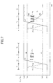
- FIG. 7 is a diagram showing waveforms in a read operation where a high level is read first and subsequently a low level is read out in the circuit configuration of FIG. 6 ;
- FIG. 8 is an entire configuration of a DRAM of a second embodiment
- FIG. 9 is a diagram showing a configuration required in read operation in an area including a global bit line GBL, a global sense amplifier 11 , a shared local sense amplifier 20 , and two local bit lines LBL regarding a specific example of the DRAM of the second embodiment;
- FIG. 10 is a diagram showing waveforms in a read operation where a high level is read first and subsequently a low level is read out in the circuit configuration of FIG. 9 ;
- FIG. 11 is a diagram explaining a structure of a memory cell MC of the second embodiment and its periphery.
- FIG. 1 shows an entire configuration of the DRAM of the first embodiment.
- FIG. 1 there are shown four memory cell arrays 10 , a plurality of global sense amplifiers 11 , a plurality of local sense amplifiers 12 , a plurality of global bit lines GBL, and a plurality of local bit lines LBL.
- Each memory cell array 10 includes a large number of memory cells formed at all intersections of a plurality of word lines and the plurality of local bit lines LBL intersecting therewith.
- the plurality of local bit lines LBL is regularly aligned with a pitch 2 F based on a design rule value F in a word line extending direction.
- the plurality of global bit lines GBL is also aligned with the same pitch 2 F as the local bit lines LBL.
- the local sense amplifiers 12 are arranged on both sides of the memory cell arrays 10 , and each local sense amplifier 12 amplifies a signal read from a memory cell through a predetermined local bit line LBL. As shown in FIG. 1 , one of two local bit lines LBL adjacent in the word line extending direction in the memory cell array 10 is connected to the left-side local sense amplifier 12 , while the other thereof is connected to the right-side local sense amplifier 12 . In this case, since the local bit line LBL are partitioned into sections corresponding to the arrangement of the memory cell arrays 10 , each local sense amplifier 12 depends only on one memory cell array 10 . Besides, the plurality of the local sense amplifiers 12 is aligned with a pitch 4 F in the word line extending direction.
- each global sense amplifier 11 is arranged at both ends of the four memory cell arrays 10 , and each global sense amplifier 11 further amplifies data transmitted from the local sense amplifier 12 to the global bit line GBL.
- each global bit line GBL is arranged extending over all the four memory cell arrays 10 .
- each global bit line GBL is connected to predetermined four local sense amplifiers 12 among eight local sense amplifiers 12 arranged in a line in a bit line extending direction.
- one of two global bit lines GBL adjacent in the memory cell array 10 is connected to the left-side global sense amplifier 11 , while the other thereof is connected to the right-side global sense amplifier 11 .
- the plurality of global sense amplifiers 11 is also aligned with the pitch 4 F in the word line extending direction.
- m/2 local sense amplifiers 12 connected to m/2 local bit lines LBL are arranged on each of both sides of the memory cell array 10 .
- 4m local sense amplifiers 12 in total are arranged in eight rows, and m global sense amplifiers 11 in total are arranged in two rows (at both ends).
- the memory cell array 10 since the memory cell array 10 is configured hierarchically, an increase in the number of memory cells connected to one local bit line LBL can be suppressed.
- data of 4n memory cells can be transmitted selectively through the global bit line GBL, but n memory cells connected to the local bit line LBL are only required.
- an overall bit line resistance can be suppressed even when the local bit line LBL is formed of material having a relatively large resistance value.
- the memory cell array 10 shown in FIG. 2 includes a plurality of memory cells MC formed at all intersections of n word lines WL (WL 1 to WLn) and m local bit lines LBL, and each memory cell MC is composed of an NMOS transistor N 0 and a capacitor C 0 . Since m ⁇ n memory cells MC are arranged in one memory cell array 10 , the memory cell array 10 becomes capable of storing m ⁇ n bit data in total.
- One end (source) of the NMOS transistor N 0 of each memory cell MC is connected to the local bit line LBL, and the other end (drain) thereof is connected to an accumulation electrode of the capacitor C 0 .
- a predetermined fixed potential is applied to an opposite electrode of the capacitor C 0 .
- This fixed potential is set to, for example, an intermediate voltage between a power supply voltage and a ground potential.
- a word line WL is connected to a gate electrode of the NMOS transistor N 0 .
- FIG. 3 shows a schematic sectional structure of the memory cell MC in the memory cell array 10 .
- the capacitor C 0 of the memory cell MC is disposed at an upper portion, and has an inside opposite electrode 101 and an outside accumulation electrode 102 , which are opposed to each other via a dielectric film 103 .
- the opposite electrode 101 is connected to a wiring for supplying the predetermined fixed potential which is included in a wiring layer (not shown) arranged in an upper portion.
- a drain region 108 at a lower portion of the capacitor C 0 , there are arranged a drain region 108 , a channel region 104 and a source region 105 in the order from an upper side, and a gate electrode 106 is formed around the channel region 104 via a gate oxide film 107 , respectively as a vertical transistor structure.
- the drain region 108 is connected to the accumulation electrode 102 of the capacitor C 0 and the source region 105 is directly connected to the local bit line LBL of a lower layer.
- the gate electrode 106 is directly connected to the word line WL.
- the local bit line LBL is formed using polysilicon or a diffusion layer and has a relatively high resistance.
- the above structure of the memory cell MC is repeatedly arranged with a predetermined interval.
- an inter insulation film (not shown) is filled between adjacent memory cells MC. Since the interval of memory cells MC is constant, the length of the local bit line LBL is determined depending on the number of connected memory cells MC. Accordingly, an overall resistance value of the local bit line LBL changes approximately in proportion to the number of connected memory cells MC, and therefore it is desirable to reduce the number of memory cells MC as much as possible so as to decrease the resistance value.
- FIG. 4 shows a configuration required in the read operation in the configuration of FIG. 1 , corresponding to an area including one global bit line GBL, one local bit line LBL, one single-ended global sense amplifier 11 and one single-ended local sense amplifier 12 .
- the local sense amplifier 12 includes an amplifying NMOS transistor N 1 and a precharging NMOS transistor N 2 .
- the amplifying NMOS transistor N 1 is connected between the global bit line GBL and ground, and the gate thereof is connected to one end of the local bit line LBL.
- the plurality of memory cells MC each composed of the NMOS transistor N 0 and the capacitor C 0 is connected to the local bit line LBL, like in FIG. 2 .
- the precharging NMOS transistor N 2 is connected between the local bit line LBL and ground, and the gate thereof is connected to a precharge signal line PCL. Note that the local sense amplifier 12 actually includes a write circuit (not shown) required for write operation.
- the global sense amplifier 11 includes a precharging PMOS transistor P 1 .
- the precharging PMOS transistor P 1 is connected between a power supply voltage VDL and the global bit line GBL, and the gate thereof is connected to a precharge signal line/PCG.
- the symbol/attached to each signal name means negative logic.
- the global sense amplifier 11 actually includes an input/output circuit (not shown) connected to input/output lines.
- the precharge signal line PCL of the local sense amplifier 12 is controlled to be high, and the precharge signal line/PCG of the global sense amplifier 11 is controlled to be low.
- the local bit line LBL is precharged to a ground potential VSS, and the global bit line GBL is precharged to the power supply voltage VDL.
- the precharge signal line PCL is controlled to be low and the precharge signal line/PCG is controlled to be high.
- FIG. 5 shows waveforms in a read operation where a high level is read out from a selected memory cell MC first and subsequently a low level is read out from the selected memory cell MC in the configuration of FIG. 4 .
- Four terms (T 1 to T 4 ) into which one read operation is divided are shown in the upper side of FIG. 5 .
- the precharge signal line PCL is controlled to be high and the precharge signal line/PCG is controlled to be low.
- the local bit line LBL is precharged to low and the global bit line GBL is precharged to high.
- the precharge signal line PCL changes from high to low in order to cancel the precharge state of the local bit line LBL
- the precharge signal line/PCG changes from low to high in order to cancel the precharge state of the global bit line GBL.
- the word line WL selected corresponding to the target memory cell MC rises from a negative voltage VKK to a positive voltage VPA.
- the negative voltage VKK is set to a value lower than “low level” (ground potential VSS), and the positive voltage VPA is set to a value higher than “high level” (power supply voltage VDL).
- VSS ground potential
- VDL power supply voltage
- the voltage Vx of the local bit line LBL is set to a value higher than at least a threshold voltage range Rvn (represented by hatching in FIG. 5 ) of the amplifying NMOS transistor N 1 .
- the threshold voltage range Rvn is distributed within a predetermined voltage range depending on temperature or process fluctuation.
- the level of the global bit line GBL falls from high to low via the amplifying NMOS transistor N 1 which has turned on. Meanwhile, the low level of the global bit line GBL is inverted by the write circuit (not shown) of the local sense amplifier 12 so as to increase the potential of the local bit line LBL, which gradually changes from the above voltage Vx to the level of the power supply voltage VDL.
- the low level is read out to the input/output lines through the input/output circuit (not shown) of the global sense amplifier 11 . Thereby, one read operation of the DRAM is completed.
- waveforms in the read operation are shown in the same manner, in which data of low level stored in the memory cell MC is read out.
- the waveforms during the precharge cancel period T 1 is the same as in the first half of FIG. 5 .
- the signal of low level stored in the memory cell MC is read out, and thus the local bit line LBL continues to remain low.
- the global bit line GBL remains high by inverting the low level of the local bit line LBL.
- the high level is read out to the input/output lines in the above described manner.
- FIG. 6 shows an example in which the configuration of the local sense amplifier 12 and the global sense amplifier 11 is modified in the same area as shown in FIG. 4 .
- one local bit line LBL, the plurality of memory cells MC connected thereto, and one global bit line GBL are arranged in the same manner as FIG. 4 .
- the local sense amplifier 12 includes an amplifying PMOS transistor P 11 and a precharging PMOS transistor P 12 .
- the amplifying PMOS transistor P 11 is connected between the power supply voltage VDL and the global bit line GBL, and the gate thereof is connected to one end of the local bit line LBL.
- the precharging PMOS transistor P 12 is connected between the power supply voltage VDL and the local bit line LBL, and the gate thereof is connected to a precharge signal line/PCL.
- the local sense amplifier 12 of FIG. 6 is configured by replacing the two NMOS transistors N 1 and N 2 of the local sense amplifier 12 of FIG. 4 with the two PMOS transistors P 11 and P 12 .
- the global sense amplifier 11 includes a precharging NMOS transistor N 11 .
- the precharging NMOS transistor N 11 is connected between the global bit line GBL and ground, and the gate thereof is connected to a precharge signal line PCG.
- the global sense amplifier 11 of FIG. 6 is configured by replacing the precharging PMOS transistor P 1 of FIG. 4 with the precharging NMOS transistor N 11 .
- the precharge signal line/PCL of the local sense amplifier 12 is controlled to be low, and the precharge signal line PCG of the global sense amplifier 11 is controlled to be high.
- the local bit line LBL is precharged to the power supply voltage VDL
- the global bit line GBL is precharged to the ground potential VSS.
- the precharge signal line/PCL is controlled to be high and the precharge signal line PCG is controlled to be low.
- FIG. 7 shows waveforms in a read operation where a high level is read out from a selected memory cell MC first and subsequently a low level is read out from the selected memory cell MC in the configuration of FIG. 6 .
- the four terms (T 1 to T 4 ) shown in the upper side of FIG. 7 have the same meanings as FIG. 5 . Most of the waveforms are common to those in FIG. 5 , and thus only different points will be mainly described below.
- the precharge signal line/PCL is controlled to be low and the precharge signal line PCG is controlled to be high.
- the local bit line LBL is precharged to high and the global bit line GBL is precharged to low.
- the word line WL changes in the same manner as in FIG. 5 .
- a signal of high level stored in the memory cell MC is read out, and thus the local bit line LBL continues to remain high.
- a threshold voltage range Rvp represented by hatching in FIG. 7
- the global bit line GBL remains low by inverting the high level of the local bit line LBL during the sensing period T 3 .
- the low level is read out to the input/output lines via the above input/output circuit (not shown).
- waveforms in the read operation are shown in the same manner, in which data of low level in the memory cell MC is read out.
- the waveforms during the precharge cancel period T 1 is the same as in the first half of FIG. 7 .
- the signal of low level stored in the memory cell MC is read out and input to the local sense amplifier 12 , thereby decreasing the local bit line LBL to a voltage Vy from the power supply voltage VDL.
- the voltage Vy of the local bit line LBL is set to a value lower than at least the above threshold voltage range Rvp of the amplifying PMOS transistor P 11 .
- the global bit line GBL rises from low to high via the amplifying PMOS transistor P 11 which has turned on during the sensing period T 3 .
- the high level of the global bit line GBL is inverted by the write circuit (not shown) of the local sense amplifier 12 so as to decrease the potential of the local bit line LBL, which gradually changes from the above voltage Vy to the ground potential VSS.
- the read period T 4 in a state where the local bit line LBL remains low and the global bit line GBL remains high, the high level is read out to the input/output lines via the above input/output circuit (not shown).
- the configuration of the first embodiment it is possible to prevent a decrease in operation speed caused by an increase in the bit line resistance when a signal read from the memory cell MC is transmitted through the local bit lines LBL.
- the polysilicon or the diffusion layer used in the embedded bit line structure has a larger resistance than that of metal or silicide, however the first embodiment requires a small number of memory cells MC connected to the local bit line LBL, and correspondingly the bit line resistance can be suppressed.
- the vertical transistor structure is employed for each memory cell MC, it is suitable for arranging the memory cells MC with higher density.
- the single-ended local sense amplifier 12 is employed, the circuit scale can be small so that an increase in the entire chip area can be prevented.
- FIG. 8 shows an entire configuration of the DRAM of the second embodiment.
- FIG. 8 there are shown four memory cell arrays 10 , a plurality of global sense amplifiers 11 , a plurality of shared local sense amplifiers 20 , a plurality of non-shared local sense amplifiers 21 , a plurality of global bit lines GBL, and a plurality of local bit lines LBL.
- FIG. 8 configurations of the four memory cell arrays 10 and the plurality of global sense amplifiers 11 are common to those of FIG. 1 .
- three shared local sense amplifiers 20 are arranged between memory cell arrays 10
- two non-shared local sense amplifiers 21 are arranged at both ends of the four memory cell arrays 10 .
- Two local bit lines LBL included in memory cell arrays 10 on both sides are connected to each local sense amplifier 20 , and a signal read out from selected one local bit line LBL is amplified by the local sense amplifier 20 .
- FIG. 9 shows a configuration required in the read operation in the configuration of FIG. 8 , corresponding to an area including one global bit line GBL, one single-ended global sense amplifier 11 , one single-ended shared local sense amplifier 20 , and two local bit lines LBL on both sides of the local sense amplifier 20 .
- the local sense amplifier 20 includes NMOS transistors N 10 and N 12 as switching circuits, in addition to an amplifying NMOS transistor N 1 and a precharging NMOS transistor N 2 which are the same as in FIG. 2 .
- the NMOS transistor N 10 is connected between one local bit line LBL and the gate of the amplifying NMOS transistor N 1 , and has a gate connected to a switching signal line SHL.
- the NMOS transistor N 12 is connected between the other local bit line LBL and the gate of the amplifying NMOS transistor N 1 , and has a gate connected to a switching signal line SHR.
- This local bit line LBLs inside a sense amplifier has a different structure from that of the two local bit lines LBL on the both sides, which will be described later in detail.
- the local bit line LBLs inside a sense amplifier can be selectively connected to either of the local bit lines LBL via one of the NMOS transistors N 10 and N 12 on the both sides, which is controlled to be in an ON state.
- one of the switching signal lines SHR and SHL is controlled to be high and the other thereof is controlled to be low, corresponding to a selected memory cell array 10 .
- each of the two local sense amplifiers 21 at both ends in FIG. 8 is configured to include either of the two NMOS transistors N 10 and N 12 in the configuration of FIG. 9 . That is, one local sense amplifier 21 includes the NMOS transistor N 10 whose gate is connected to the switching signal line SHL, and the other local sense amplifier 21 includes the NMOS transistor N 12 whose gate is connected to the switching signal line SHR.
- FIG. 10 shows waveforms in a read operation where a high level is read out from a selected memory cell MC first and subsequently a low level is read out from the selected memory cell MC in the configuration of FIG. 9 .
- a case where the left side memory cell array 10 is selected is assumed.
- Four terms (T 1 to T 4 ) in the upper side of FIG. 10 have the same meanings as in FIG. 5 .
- Most of the waveforms in FIG. 10 are common to those in FIG. 5 , and thus only different points will be mainly described below.
- T 1 in the first half of FIG. 10 one switching signal line SHR changes from high to low and the other switching signal line SHL remains in a high state.
- the switching signal lines SHL and SHR are controlled to be the positive voltage VPA and the ground potential VSS.
- the local sense amplifier 20 on the right side of the selected memory cell array 10 becomes in a state where the left side transistor N 10 is ON and the right side transistor N 12 is OFF.
- the amplifying NMOS transistor N 1 is connected to the left side local bit line LBL through the local bit line LBLs inside a sense amplifier.
- the waveforms changes in the same manner as in the first half.
- the waveforms of the switching signal lines SHL and SHR are replaced with each other in FIG. 10 .
- FIG. 11 shows a sectional structure of an area including a memory cell array region and a sense amplifier region which are shown in FIG. 9 .
- the sectional structure of the memory cell MC in the memory cell array region is the same as in FIG. 3 , so description thereof is omitted.
- the NMOS transistor N 10 of the local sense amplifier 12 is formed in a vicinity of a boundary between the memory cell array region and the sense amplifier region.
- This NMOS transistor N 10 has the vertical transistor structure in the same manner as the NMOS transistor N 0 of the memory cell MC.
- a source region 105 directly connected to the lower local bit line LBL, a channel region 104 around which a gate electrode 106 is formed via a gate oxide film 107 , and a drain region 108 , in the order from a lower layer.
- the drain region 108 is connected to one end of the local bit line LBLs inside a sense amplifier arranged in an upper portion via a contact 109 .
- the NMOS transistor N 12 At the other end of the local bit line LBLs inside a sense amplifier, there are formed the NMOS transistor N 12 having the same transistor structure, and the source region 105 thereof is directly connected to the other local bit line LBL. Note that other MOS transistors in the sense amplifier region are formed with a normal plane structure.
- the NMOS transistors N 10 and N 12 as switching circuits of the local sense amplifier 20 can be formed with the vertical transistor structure in the same manner as the NMOS transistor N 0 of the memory cell MC.
- a signal path of the local bit line LBL is lifted from a lower layer to an upper layer and connected to the local bit line LBLs inside a sense amplifier, by the vertical transistor structure of the NMOS transistors N 10 and N 12 and the contact 109 .
- the vertical transistor structure can be employed for the two NMOS transistors N 10 and N 12 in the local sense amplifier 20 , thereby reducing a corresponding area.
- the entire area of the semiconductor memory device can be sufficiently reduced.
- the effect of the second embodiment to prevent a reduction in the operation speed caused by an increase in the bit line resistance of each local bit line LBL is the same as the first embodiment.
- the present invention has been specifically described based on the two embodiments.
- the present invention is not limited to the above described embodiments, and can be variously modified without departing the essentials of the present invention.
- N is an integer greater than or equal to two
- the number of memory cells MC connected to one local bit line LBL can be reduced.
- the number of memory cells MC in total becomes large in a large capacity DRAM, it is desirable to reduce the number of memory cells MC by partitioning the local bit lines LBL into small sections as much as possible so as to reduce the bit line resistance.
Landscapes
- Engineering & Computer Science (AREA)
- Microelectronics & Electronic Packaging (AREA)
- Computer Hardware Design (AREA)
- Dram (AREA)
- Semiconductor Memories (AREA)
Abstract
Description
Claims (8)
Applications Claiming Priority (2)
| Application Number | Priority Date | Filing Date | Title |
|---|---|---|---|
| JP2007139735A JP2008294310A (en) | 2007-05-25 | 2007-05-25 | Semiconductor memory device |
| JP2007-139735 | 2007-05-25 |
Publications (2)
| Publication Number | Publication Date |
|---|---|
| US20080291764A1 US20080291764A1 (en) | 2008-11-27 |
| US7701794B2 true US7701794B2 (en) | 2010-04-20 |
Family
ID=40072264
Family Applications (1)
| Application Number | Title | Priority Date | Filing Date |
|---|---|---|---|
| US12/127,198 Expired - Fee Related US7701794B2 (en) | 2007-05-25 | 2008-05-27 | Semiconductor memory device |
Country Status (2)
| Country | Link |
|---|---|
| US (1) | US7701794B2 (en) |
| JP (1) | JP2008294310A (en) |
Cited By (8)
| Publication number | Priority date | Publication date | Assignee | Title |
|---|---|---|---|---|
| US20090257268A1 (en) * | 2008-03-17 | 2009-10-15 | Elpida Memory, Inc. | Semiconductor device having single-ended sensing amplifier |
| US8472272B2 (en) | 2010-11-04 | 2013-06-25 | Elpida Memory Inc. | Semiconductor device having hierarchical bit line structure |
| US8593860B2 (en) | 2011-12-09 | 2013-11-26 | Gsi Technology, Inc. | Systems and methods of sectioned bit line memory arrays |
| US8665625B2 (en) | 2009-07-30 | 2014-03-04 | Elpida Memory, Inc. | Semiconductor device having hierarchically structured bit lines and system including the same |
| US8693236B2 (en) | 2011-12-09 | 2014-04-08 | Gsi Technology, Inc. | Systems and methods of sectioned bit line memory arrays, including hierarchical and/or other features |
| US9224487B2 (en) | 2010-04-16 | 2015-12-29 | Cypress Semiconductor Corporation | Semiconductor memory read and write access |
| USRE46110E1 (en) | 2008-03-17 | 2016-08-16 | Ps4 Luxco S.A.R.L. | Semiconductor device having single-ended sensing amplifier |
| US20210028176A1 (en) * | 2019-07-25 | 2021-01-28 | Micron Technology, Inc. | Memory arrays with vertical access transistors |
Families Citing this family (5)
| Publication number | Priority date | Publication date | Assignee | Title |
|---|---|---|---|---|
| JP2008282459A (en) * | 2007-05-08 | 2008-11-20 | Elpida Memory Inc | Semiconductor storage device |
| JP5666108B2 (en) * | 2009-07-30 | 2015-02-12 | ピーエスフォー ルクスコ エスエイアールエルPS4 Luxco S.a.r.l. | Semiconductor device and system including the same |
| WO2014080756A1 (en) * | 2012-11-22 | 2014-05-30 | ピーエスフォー ルクスコ エスエイアールエル | Semiconductor device |
| US9542980B1 (en) * | 2016-03-29 | 2017-01-10 | Nanya Technology Corp. | Sense amplifier with mini-gap architecture and parallel interconnect |
| US11114446B2 (en) * | 2016-12-29 | 2021-09-07 | Intel Corporation | SRAM with hierarchical bit lines in monolithic 3D integrated chips |
Citations (6)
| Publication number | Priority date | Publication date | Assignee | Title |
|---|---|---|---|---|
| JPH07321228A (en) | 1994-05-26 | 1995-12-08 | Mitsubishi Electric Corp | Semiconductor device and manufacturing method thereof |
| US20020030214A1 (en) | 2000-09-11 | 2002-03-14 | Fumio Horiguchi | Semiconductor device and method for manufacturing the same |
| US6452851B1 (en) * | 1998-10-29 | 2002-09-17 | Hitachi, Ltd. | Semiconductor integrated circuit device |
| US6646954B2 (en) * | 2001-02-02 | 2003-11-11 | Broadcom Corporation | Synchronous controlled, self-timed local SRAM block |
| US6937535B2 (en) * | 2002-10-29 | 2005-08-30 | Hynix Semiconductor Inc. | Semiconductor memory device with reduced data access time |
| US7200061B2 (en) * | 2002-11-08 | 2007-04-03 | Hitachi, Ltd. | Sense amplifier for semiconductor memory device |
Family Cites Families (6)
| Publication number | Priority date | Publication date | Assignee | Title |
|---|---|---|---|---|
| JPS63228496A (en) * | 1987-03-17 | 1988-09-22 | Fujitsu Ltd | memory circuit |
| JPH04153977A (en) * | 1990-10-17 | 1992-05-27 | Hitachi Ltd | semiconductor memory |
| JP3626510B2 (en) * | 1993-04-13 | 2005-03-09 | 株式会社ルネサステクノロジ | Semiconductor memory device |
| JPH0878635A (en) * | 1994-08-31 | 1996-03-22 | Toshiba Corp | Semiconductor memory device |
| JP3266850B2 (en) * | 1997-03-27 | 2002-03-18 | 松下電器産業株式会社 | Semiconductor memory |
| JP2004234760A (en) * | 2003-01-30 | 2004-08-19 | Renesas Technology Corp | Semiconductor memory |
-
2007
- 2007-05-25 JP JP2007139735A patent/JP2008294310A/en not_active Withdrawn
-
2008
- 2008-05-27 US US12/127,198 patent/US7701794B2/en not_active Expired - Fee Related
Patent Citations (8)
| Publication number | Priority date | Publication date | Assignee | Title |
|---|---|---|---|---|
| JPH07321228A (en) | 1994-05-26 | 1995-12-08 | Mitsubishi Electric Corp | Semiconductor device and manufacturing method thereof |
| JP3745392B2 (en) | 1994-05-26 | 2006-02-15 | 株式会社ルネサステクノロジ | Semiconductor device |
| US6452851B1 (en) * | 1998-10-29 | 2002-09-17 | Hitachi, Ltd. | Semiconductor integrated circuit device |
| US20020030214A1 (en) | 2000-09-11 | 2002-03-14 | Fumio Horiguchi | Semiconductor device and method for manufacturing the same |
| JP2002094027A (en) | 2000-09-11 | 2002-03-29 | Toshiba Corp | Semiconductor memory device and its manufacturing method |
| US6646954B2 (en) * | 2001-02-02 | 2003-11-11 | Broadcom Corporation | Synchronous controlled, self-timed local SRAM block |
| US6937535B2 (en) * | 2002-10-29 | 2005-08-30 | Hynix Semiconductor Inc. | Semiconductor memory device with reduced data access time |
| US7200061B2 (en) * | 2002-11-08 | 2007-04-03 | Hitachi, Ltd. | Sense amplifier for semiconductor memory device |
Cited By (14)
| Publication number | Priority date | Publication date | Assignee | Title |
|---|---|---|---|---|
| US20090257268A1 (en) * | 2008-03-17 | 2009-10-15 | Elpida Memory, Inc. | Semiconductor device having single-ended sensing amplifier |
| US8045360B2 (en) * | 2008-03-17 | 2011-10-25 | Elpida Memory, Inc. | Semiconductor device having single-ended sensing amplifier |
| US20120008368A1 (en) * | 2008-03-17 | 2012-01-12 | Elpida Memory, Inc. | Semiconductor device having single-ended sensing amplifier |
| US8310887B2 (en) * | 2008-03-17 | 2012-11-13 | Elpida Memory, Inc. | Semiconductor device having single-ended sensing amplifier |
| USRE46110E1 (en) | 2008-03-17 | 2016-08-16 | Ps4 Luxco S.A.R.L. | Semiconductor device having single-ended sensing amplifier |
| US8665625B2 (en) | 2009-07-30 | 2014-03-04 | Elpida Memory, Inc. | Semiconductor device having hierarchically structured bit lines and system including the same |
| US8773884B2 (en) | 2009-07-30 | 2014-07-08 | Seiji Narui | Semiconductor device having hierarchically structured bit lines and system including the same |
| US9224487B2 (en) | 2010-04-16 | 2015-12-29 | Cypress Semiconductor Corporation | Semiconductor memory read and write access |
| US8472272B2 (en) | 2010-11-04 | 2013-06-25 | Elpida Memory Inc. | Semiconductor device having hierarchical bit line structure |
| US8593860B2 (en) | 2011-12-09 | 2013-11-26 | Gsi Technology, Inc. | Systems and methods of sectioned bit line memory arrays |
| US8693236B2 (en) | 2011-12-09 | 2014-04-08 | Gsi Technology, Inc. | Systems and methods of sectioned bit line memory arrays, including hierarchical and/or other features |
| US9135986B2 (en) | 2011-12-09 | 2015-09-15 | Gsi Technology, Inc. | Systems and methods of sectioned bit line memory arrays, including hierarchical and/or other features |
| US20210028176A1 (en) * | 2019-07-25 | 2021-01-28 | Micron Technology, Inc. | Memory arrays with vertical access transistors |
| US10916548B1 (en) * | 2019-07-25 | 2021-02-09 | Micron Technology, Inc. | Memory arrays with vertical access transistors |
Also Published As
| Publication number | Publication date |
|---|---|
| JP2008294310A (en) | 2008-12-04 |
| US20080291764A1 (en) | 2008-11-27 |
Similar Documents
| Publication | Publication Date | Title |
|---|---|---|
| US7701794B2 (en) | Semiconductor memory device | |
| US7948784B2 (en) | Semiconductor memory device having vertical transistors | |
| US7697358B2 (en) | Semiconductor memory device | |
| US6636454B2 (en) | Low-power consumption semiconductor memory device | |
| US7830738B2 (en) | Semiconductor memory device | |
| JP3781270B2 (en) | Semiconductor integrated circuit device | |
| US20150255146A1 (en) | Semiconductor device including subword driver circuit | |
| US20050162894A1 (en) | Semiconductor integrated circuit device | |
| US20070121414A1 (en) | Shielded bitline architecture for dynamic random access memory (dram) arrays | |
| US10153007B2 (en) | Apparatuses including a memory array with separate global read and write lines and/or sense amplifier region column select line and related methods | |
| US7259977B2 (en) | Semiconductor device having hierarchized bit lines | |
| JP2007042172A (en) | Semiconductor memory apparatus | |
| US20070058418A1 (en) | Semiconductor memory device having memory cells requiring no refresh operation | |
| JP2009033029A (en) | Semiconductor memory device | |
| US8976563B2 (en) | Semiconductor memory device | |
| US8107278B2 (en) | Semiconductor storage device | |
| US10706917B2 (en) | Semiconductor memory device | |
| US9741397B2 (en) | Semiconductor memory device | |
| KR100801710B1 (en) | A nonvolatile memory device and a memory system including the device. | |
| US5666306A (en) | Multiplication of storage capacitance in memory cells by using the Miller effect | |
| CN102024816B (en) | Semiconductor memory device | |
| US9251871B2 (en) | Sense amplifier with dual gate precharge and decode transistors | |
| US8542547B2 (en) | Semiconductor device and data processing system | |
| US6765253B2 (en) | Semiconductor memory device | |
| US7649799B2 (en) | Semiconductor memory device |
Legal Events
| Date | Code | Title | Description |
|---|---|---|---|
| AS | Assignment |
Owner name: ELPIDA MEMORY, INC., JAPAN Free format text: ASSIGNMENT OF ASSIGNORS INTEREST;ASSIGNOR:KAJIGAYA, KAZUHIKO;REEL/FRAME:021001/0022 Effective date: 20080512 Owner name: ELPIDA MEMORY, INC.,JAPAN Free format text: ASSIGNMENT OF ASSIGNORS INTEREST;ASSIGNOR:KAJIGAYA, KAZUHIKO;REEL/FRAME:021001/0022 Effective date: 20080512 |
|
| AS | Assignment |
Owner name: ELPIDA MEMORY INC., JAPAN Free format text: SECURITY AGREEMENT;ASSIGNOR:PS4 LUXCO S.A.R.L.;REEL/FRAME:032414/0261 Effective date: 20130726 |
|
| FPAY | Fee payment |
Year of fee payment: 4 |
|
| AS | Assignment |
Owner name: PS4 LUXCO S.A.R.L., LUXEMBOURG Free format text: ASSIGNMENT OF ASSIGNORS INTEREST;ASSIGNOR:ELPIDA MEMORY, INC.;REEL/FRAME:032899/0588 Effective date: 20130726 |
|
| FEPP | Fee payment procedure |
Free format text: PAYOR NUMBER ASSIGNED (ORIGINAL EVENT CODE: ASPN); ENTITY STATUS OF PATENT OWNER: LARGE ENTITY |
|
| AS | Assignment |
Owner name: PS5 LUXCO S.A.R.L., LUXEMBOURG Free format text: ASSIGNMENT OF ASSIGNORS INTEREST;ASSIGNOR:PS4 LUXCO S.A.R.L.;REEL/FRAME:039818/0506 Effective date: 20130829 Owner name: LONGITUDE SEMICONDUCTOR S.A.R.L., LUXEMBOURG Free format text: CHANGE OF NAME;ASSIGNOR:PS5 LUXCO S.A.R.L.;REEL/FRAME:039793/0880 Effective date: 20131112 |
|
| FEPP | Fee payment procedure |
Free format text: MAINTENANCE FEE REMINDER MAILED (ORIGINAL EVENT CODE: REM.) |
|
| LAPS | Lapse for failure to pay maintenance fees |
Free format text: PATENT EXPIRED FOR FAILURE TO PAY MAINTENANCE FEES (ORIGINAL EVENT CODE: EXP.) |
|
| STCH | Information on status: patent discontinuation |
Free format text: PATENT EXPIRED DUE TO NONPAYMENT OF MAINTENANCE FEES UNDER 37 CFR 1.362 |
|
| FP | Lapsed due to failure to pay maintenance fee |
Effective date: 20180420 |