US7698607B2 - Repairing microdisplay frame buffers - Google Patents
Repairing microdisplay frame buffers Download PDFInfo
- Publication number
- US7698607B2 US7698607B2 US10/868,057 US86805704A US7698607B2 US 7698607 B2 US7698607 B2 US 7698607B2 US 86805704 A US86805704 A US 86805704A US 7698607 B2 US7698607 B2 US 7698607B2
- Authority
- US
- United States
- Prior art keywords
- cell
- defective
- frame buffer
- adjacent
- array
- Prior art date
- Legal status (The legal status is an assumption and is not a legal conclusion. Google has not performed a legal analysis and makes no representation as to the accuracy of the status listed.)
- Expired - Fee Related, expires
Links
Images


Classifications
-
- G—PHYSICS
- G11—INFORMATION STORAGE
- G11C—STATIC STORES
- G11C29/00—Checking stores for correct operation ; Subsequent repair; Testing stores during standby or offline operation
- G11C29/70—Masking faults in memories by using spares or by reconfiguring
- G11C29/78—Masking faults in memories by using spares or by reconfiguring using programmable devices
- G11C29/84—Masking faults in memories by using spares or by reconfiguring using programmable devices with improved access time or stability
- G11C29/848—Masking faults in memories by using spares or by reconfiguring using programmable devices with improved access time or stability by adjacent switching
-
- G—PHYSICS
- G09—EDUCATION; CRYPTOGRAPHY; DISPLAY; ADVERTISING; SEALS
- G09G—ARRANGEMENTS OR CIRCUITS FOR CONTROL OF INDICATING DEVICES USING STATIC MEANS TO PRESENT VARIABLE INFORMATION
- G09G3/00—Control arrangements or circuits, of interest only in connection with visual indicators other than cathode-ray tubes
- G09G3/006—Electronic inspection or testing of displays and display drivers, e.g. of LED or LCD displays
-
- G—PHYSICS
- G09—EDUCATION; CRYPTOGRAPHY; DISPLAY; ADVERTISING; SEALS
- G09G—ARRANGEMENTS OR CIRCUITS FOR CONTROL OF INDICATING DEVICES USING STATIC MEANS TO PRESENT VARIABLE INFORMATION
- G09G2360/00—Aspects of the architecture of display systems
- G09G2360/18—Use of a frame buffer in a display terminal, inclusive of the display panel
Definitions
- This invention relates generally to microdisplays for displaying information in association with processor-based systems.
- a microdisplay is a relatively small display which can be viewed directly, as in a head mounted display, or enlarged by using projection systems, for example. Commonly, microdisplays are less than four centimeters measured diagonally.
- Digital microdisplays may contain integrated frame buffers that hold the pixel data for the image being displayed.
- a large number of pixels may be utilized. Displaying a large number of pixels requires a relatively large frame buffer to store the data being displayed.
- the yield of an integrated circuit, which includes both the pixel array and the frame buffer, may be limited by the yield of memory that implements the frame buffer.
- the memory may contain a redundancy repair mechanism to allow the microdisplay to tolerate a certain number of failures during fabrication of the frame buffer.
- a redundancy repair mechanism to allow the microdisplay to tolerate a certain number of failures during fabrication of the frame buffer.
- the entire frame buffer need not be disposed of because redundant memory blocks may be utilized to replace blocks that have damaged memory location.
- the memory may be tightly coupled to the pixel array that forms the display.
- the physical layout of the bits is constrained by the size and location of the pixels. That is, the memory for a pixel at some location may be adjacent to the memory for a pixel at another location.
- FIG. 1 is a schematic depiction of a system in accordance with one embodiment of the present invention
- FIG. 2 is a schematic depiction of a microdisplay in accordance with one embodiment of the present invention.
- FIG. 3 is a schematic depiction of a frame buffer in one embodiment of the present invention.
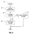
- FIG. 4 is a flow chart for one embodiment of the present invention.
- a processor-based system 100 may include a microdisplay 108 .
- the system 100 may, for example, be a projection display or a head mounted display system.
- the microdisplay 108 may be coupled by a display controller 106 to a bus 104 .
- the bus 104 in one architecture, may be coupled to an input/output device 110 and a storage 112 .
- the storage 112 may include dynamic random access memory in one embodiment.
- the bus 104 may also be coupled to a processor 102 . While a simple architecture for a processor-based system 100 is illustrated, the present invention is in no way limited to any particular architecture.
- the microdisplay 108 may include a display driver 118 coupled to a memory array 116 and an integrated circuit 114 .
- the integrated circuit 114 includes a frame buffer 10 coupled to display drive circuits 118 , in turn coupled to a pixel array 116 .
- the pixel array 116 and the frame buffer 10 may be organized in the same fashion so that each pixel in the array 116 corresponds to similarly located memory location in the frame buffer 10 .
- the frame buffer 10 of an integrated microdisplay 108 may include control logic 12 and a series of multiplexers 14 .
- the multiplexers 14 receive control signals from the control logic 12 and column values from an appropriate address buffer (not shown).
- the control logic 12 may receive address and failure information.
- a column of memory cells or bits is located below each multiplexer 14 .
- column X may include memory cells (X, Y), (X, Y+1) and so on.
- column X+1 may be coupled to a multiplexer 14 which, in turn, is coupled to a column including memory cells (X+1, Y), (X+1, Y+1) and so on.
- the cells in the frame buffer 10 are arranged in an addressable array made up of two sets of generally transverse lines. One set may be considered column lines and the other set may be considered as row lines. Each cell can be accessed by addressing a particular line in each set of lines.
- the multiplexer 14 may be coupled to its column by a line 20 . That multiplexer 14 is also coupled by a line 18 to an adjacent column X+3.
- adjacent pixels in an image tend to have similar values in typical images. That is, if a pixel at location (X, Y) has an intensity value of 50, it is likely that a pixel at location (X+1, Y) has a value around 50 as well.
- the replacement will not be noticeable by the user. Since the value that is replaced may either be a color component value, an intermediate value that applied to the modulation of the pixel, or other such pixel specific information that represents a pixel value, it is generally the case that adjacent pixels will have sufficiently similar values that the replacement is not noticeable.
- control logic 12 may select an adjacent column, in one embodiment of the present invention, when a cell at a particular row and column address is known to be defective. In other words, when normally the cell (X+2, Y) would be addressed, when the control logic 12 has information that that cell is defective, the multiplexer 14 accesses the value from the adjacent column, same row (X+3, Y).
- Each multiplexer 14 is controlled or programmed by the control logic 12 based on the information the control logic 12 receives about bad cells. This information may be programmed into the microdisplay 108 based on post-fabrication testing. Thus, when a cell in a column is bad, the replacement information is accessed over the line 18 . When the addressed cell is good, it is accessed via a line 20 by an overlying multiplexer 14 . Thus, some cells may be accessed two or more times to refresh the display.
- a repair algorithm 22 may be implemented in hardware or software. Initially, the address information with the defective cells identified is received as indicated in block 24 . The failure location is determined as indicated in diamond 26 . If an address location is a failure location, a corresponding cell in a next column, same row, may be addressed as indicated in block 28 . In other words, the information stored on the adjacent cell is used in place of the information stored on the address cell. If there is no failure, then an addressed cell is accessed as indicated in block 30 .
- the coupling that is desirable in a microdisplay between the pixel locations and the memory locations can be achieved without sacrificing the ability to repair the memory. In some embodiments of the present invention, this results in better uniformity than would be the case with redundant blocks or redundant cells.
Abstract
Description
Claims (13)
Priority Applications (1)
| Application Number | Priority Date | Filing Date | Title |
|---|---|---|---|
| US10/868,057 US7698607B2 (en) | 2004-06-15 | 2004-06-15 | Repairing microdisplay frame buffers |
Applications Claiming Priority (1)
| Application Number | Priority Date | Filing Date | Title |
|---|---|---|---|
| US10/868,057 US7698607B2 (en) | 2004-06-15 | 2004-06-15 | Repairing microdisplay frame buffers |
Publications (2)
| Publication Number | Publication Date |
|---|---|
| US20050278582A1 US20050278582A1 (en) | 2005-12-15 |
| US7698607B2 true US7698607B2 (en) | 2010-04-13 |
Family
ID=35461915
Family Applications (1)
| Application Number | Title | Priority Date | Filing Date |
|---|---|---|---|
| US10/868,057 Expired - Fee Related US7698607B2 (en) | 2004-06-15 | 2004-06-15 | Repairing microdisplay frame buffers |
Country Status (1)
| Country | Link |
|---|---|
| US (1) | US7698607B2 (en) |
Cited By (3)
| Publication number | Priority date | Publication date | Assignee | Title |
|---|---|---|---|---|
| US20120246379A1 (en) * | 2011-03-25 | 2012-09-27 | Nvidia Corporation | Techniques for different memory depths on different partitions |
| US9424383B2 (en) | 2011-04-11 | 2016-08-23 | Nvidia Corporation | Design, layout, and manufacturing techniques for multivariant integrated circuits |
| US9529712B2 (en) | 2011-07-26 | 2016-12-27 | Nvidia Corporation | Techniques for balancing accesses to memory having different memory types |
Families Citing this family (1)
| Publication number | Priority date | Publication date | Assignee | Title |
|---|---|---|---|---|
| US7019884B2 (en) * | 2003-03-31 | 2006-03-28 | Intel Corporation | Light modulator with bi-directional drive |
Citations (10)
| Publication number | Priority date | Publication date | Assignee | Title |
|---|---|---|---|---|
| US4734774A (en) * | 1981-08-14 | 1988-03-29 | Texas Instruments Incorporated | CCD imager video output defect compensation |
| US5784040A (en) * | 1992-09-30 | 1998-07-21 | Sanyo Electric Co., Ltd. | Image information processor |
| US6445602B1 (en) * | 1998-10-28 | 2002-09-03 | Nucore Technology Inc. | Structure and method for correction of defective analog data in a nonvolatile semiconductor memory |
| US6456339B1 (en) * | 1998-07-31 | 2002-09-24 | Massachusetts Institute Of Technology | Super-resolution display |
| US6518945B1 (en) * | 1997-07-25 | 2003-02-11 | Aurora Systems, Inc. | Replacing defective circuit elements by column and row shifting in a flat-panel display |
| US6564346B1 (en) * | 1999-12-07 | 2003-05-13 | Infineon Technologies Richmond, Lp. | Advanced bit fail map compression with fail signature analysis |
| US20040096125A1 (en) * | 2002-11-15 | 2004-05-20 | Timothy Alderson | Method and apparatus for image processing using weighted defective pixel replacement |
| US20050024981A1 (en) * | 2002-12-05 | 2005-02-03 | Intel Corporation. | Byte aligned redundancy for memory array |
| US6934208B2 (en) * | 2002-12-03 | 2005-08-23 | Boise Technology, Inc. | Apparatus and method for a current limiting bleeder device shared by columns of different memory arrays |
| US20060176401A1 (en) * | 2002-10-24 | 2006-08-10 | Turchetta Renato Andrea D | Imaging device |
-
2004
- 2004-06-15 US US10/868,057 patent/US7698607B2/en not_active Expired - Fee Related
Patent Citations (10)
| Publication number | Priority date | Publication date | Assignee | Title |
|---|---|---|---|---|
| US4734774A (en) * | 1981-08-14 | 1988-03-29 | Texas Instruments Incorporated | CCD imager video output defect compensation |
| US5784040A (en) * | 1992-09-30 | 1998-07-21 | Sanyo Electric Co., Ltd. | Image information processor |
| US6518945B1 (en) * | 1997-07-25 | 2003-02-11 | Aurora Systems, Inc. | Replacing defective circuit elements by column and row shifting in a flat-panel display |
| US6456339B1 (en) * | 1998-07-31 | 2002-09-24 | Massachusetts Institute Of Technology | Super-resolution display |
| US6445602B1 (en) * | 1998-10-28 | 2002-09-03 | Nucore Technology Inc. | Structure and method for correction of defective analog data in a nonvolatile semiconductor memory |
| US6564346B1 (en) * | 1999-12-07 | 2003-05-13 | Infineon Technologies Richmond, Lp. | Advanced bit fail map compression with fail signature analysis |
| US20060176401A1 (en) * | 2002-10-24 | 2006-08-10 | Turchetta Renato Andrea D | Imaging device |
| US20040096125A1 (en) * | 2002-11-15 | 2004-05-20 | Timothy Alderson | Method and apparatus for image processing using weighted defective pixel replacement |
| US6934208B2 (en) * | 2002-12-03 | 2005-08-23 | Boise Technology, Inc. | Apparatus and method for a current limiting bleeder device shared by columns of different memory arrays |
| US20050024981A1 (en) * | 2002-12-05 | 2005-02-03 | Intel Corporation. | Byte aligned redundancy for memory array |
Cited By (4)
| Publication number | Priority date | Publication date | Assignee | Title |
|---|---|---|---|---|
| US20120246379A1 (en) * | 2011-03-25 | 2012-09-27 | Nvidia Corporation | Techniques for different memory depths on different partitions |
| US9477597B2 (en) * | 2011-03-25 | 2016-10-25 | Nvidia Corporation | Techniques for different memory depths on different partitions |
| US9424383B2 (en) | 2011-04-11 | 2016-08-23 | Nvidia Corporation | Design, layout, and manufacturing techniques for multivariant integrated circuits |
| US9529712B2 (en) | 2011-07-26 | 2016-12-27 | Nvidia Corporation | Techniques for balancing accesses to memory having different memory types |
Also Published As
| Publication number | Publication date |
|---|---|
| US20050278582A1 (en) | 2005-12-15 |
Similar Documents
| Publication | Publication Date | Title |
|---|---|---|
| JP4979060B2 (en) | Semiconductor integrated circuit for display control | |
| US5583822A (en) | Single chip controller-memory device and a memory architecture and methods suitable for implementing the same | |
| US7471573B2 (en) | Integrated circuit device and electronic instrument | |
| US5701270A (en) | Single chip controller-memory device with interbank cell replacement capability and a memory architecture and methods suitble for implementing the same | |
| US7616520B2 (en) | Integrated circuit device and electronic instrument | |
| US7986541B2 (en) | Integrated circuit device and electronic instrument | |
| US20050001846A1 (en) | Memory device, display control driver with the same, and display apparatus using display control driver | |
| US20080112254A1 (en) | Integrated circuit device and electronic instrument | |
| US6202180B1 (en) | Semiconductor memory capable of relieving a defective memory cell by exchanging addresses | |
| US20050219898A1 (en) | Dedicated redundancy circuits for different operations in a flash memory device | |
| US11676680B2 (en) | SRAM dynamic failure handling system using CRC and method for the same | |
| TW200837707A (en) | Semiconductor integrated circuit device for display controller | |
| US6909645B2 (en) | Cluster based redundancy scheme for semiconductor memories | |
| US7698607B2 (en) | Repairing microdisplay frame buffers | |
| US7979755B2 (en) | Semiconductor integrated circuit device for display controller | |
| US6513130B1 (en) | Circuits, systems, and methods for accounting for defective cells in a memory device | |
| US6870782B2 (en) | Row redundancy memory repair scheme with shift to eliminate timing penalty | |
| US7425961B2 (en) | Display panel driver unit | |
| US20080049038A1 (en) | Display device integrated circuit (DDI) with adaptive memory control and adaptive memory control method for DDI | |
| JP3833366B2 (en) | Image data storage device | |
| JP2007188335A (en) | Image data processor and frame memory | |
| JP2006309776A (en) | Image data storage device |
Legal Events
| Date | Code | Title | Description |
|---|---|---|---|
| AS | Assignment |
Owner name: INTEL CORPORATION, CALIFORNIA Free format text: ASSIGNMENT OF ASSIGNORS INTEREST;ASSIGNOR:WILLIS, THOMAS E.;REEL/FRAME:015482/0499 Effective date: 20040614 Owner name: INTEL CORPORATION,CALIFORNIA Free format text: ASSIGNMENT OF ASSIGNORS INTEREST;ASSIGNOR:WILLIS, THOMAS E.;REEL/FRAME:015482/0499 Effective date: 20040614 |
|
| STCF | Information on status: patent grant |
Free format text: PATENTED CASE |
|
| FEPP | Fee payment procedure |
Free format text: PAYOR NUMBER ASSIGNED (ORIGINAL EVENT CODE: ASPN); ENTITY STATUS OF PATENT OWNER: LARGE ENTITY |
|
| FPAY | Fee payment |
Year of fee payment: 4 |
|
| MAFP | Maintenance fee payment |
Free format text: PAYMENT OF MAINTENANCE FEE, 8TH YEAR, LARGE ENTITY (ORIGINAL EVENT CODE: M1552) Year of fee payment: 8 |
|
| FEPP | Fee payment procedure |
Free format text: MAINTENANCE FEE REMINDER MAILED (ORIGINAL EVENT CODE: REM.); ENTITY STATUS OF PATENT OWNER: LARGE ENTITY |
|
| LAPS | Lapse for failure to pay maintenance fees |
Free format text: PATENT EXPIRED FOR FAILURE TO PAY MAINTENANCE FEES (ORIGINAL EVENT CODE: EXP.); ENTITY STATUS OF PATENT OWNER: LARGE ENTITY |
|
| STCH | Information on status: patent discontinuation |
Free format text: PATENT EXPIRED DUE TO NONPAYMENT OF MAINTENANCE FEES UNDER 37 CFR 1.362 |
|
| FP | Lapsed due to failure to pay maintenance fee |
Effective date: 20220413 |