US7697323B2 - Magnetic storage device - Google Patents
Magnetic storage device Download PDFInfo
- Publication number
- US7697323B2 US7697323B2 US11/823,063 US82306307A US7697323B2 US 7697323 B2 US7697323 B2 US 7697323B2 US 82306307 A US82306307 A US 82306307A US 7697323 B2 US7697323 B2 US 7697323B2
- Authority
- US
- United States
- Prior art keywords
- yoke
- line
- magnetic storage
- storage device
- magneto
- Prior art date
- Legal status (The legal status is an assumption and is not a legal conclusion. Google has not performed a legal analysis and makes no representation as to the accuracy of the status listed.)
- Expired - Fee Related
Links
Images


Classifications
-
- G—PHYSICS
- G11—INFORMATION STORAGE
- G11C—STATIC STORES
- G11C11/00—Digital stores characterised by the use of particular electric or magnetic storage elements; Storage elements therefor
- G11C11/02—Digital stores characterised by the use of particular electric or magnetic storage elements; Storage elements therefor using magnetic elements
- G11C11/16—Digital stores characterised by the use of particular electric or magnetic storage elements; Storage elements therefor using magnetic elements using elements in which the storage effect is based on magnetic spin effect
Definitions
- the invention relates to a magnetic storage device which stores information in magneto-resistive elements.
- MRAM Magnetic Random Access Memory
- DRAM Dynamic Random Access Memory
- SRAM Static RAM
- MRAM Magnetic Random Access Memory
- DRAM Dynamic Random Access Memory
- SRAM Static RAM
- MRAM is superior in terms of access speed, reliability, power consumption, and the like. It can thus be said that MRAM is capable of replacing all the functions of volatile memories such as DRAM and SRAM and those of nonvolatile storing means such as flash EEPROM and hard disk units (see Japanese Patent Publication No. 3466470).
- a requirement of such ubiquitous computing includes a storage device that is capable of high speed processing with reduced power consumption and that can also avoid loss of information, even upon power-down.
- MRAM has the potential to meet both of these requirements, and is expected to be adopted by many information apparatuses in the future.
- magnetic storage devices described in Japanese Patent Application Laid-Open Nos. 2000-90658 and 2004-128430. These magnetic storage devices include, in each of their storage areas (memory cells), a bit line, a word line arranged orthogonal to the bit line, a tunneling magneto-resistive (TMR) element arranged at the intersection between the bit line and the word line, and the like. These magnetic storage devices further include a yoke (field control layer) which is arranged near each TMR element so as to surround the bit line and the word line of the same.
- TMR tunneling magneto-resistive
- the yoke is made of a ferromagnetic body having high permeability, and functions to reduce the occurrence of flux leakage from the bit line or the word line, thereby concentrating the flux into the TMR element. This makes it possible to produce a field necessary for inverting the magnetization of the TMR element, even at low power consumption.
- a TMR element includes: a first magnetic layer (magnetic sensing layer) whose direction of magnetization changes with an external field; a second magnetic layer having a fixed direction of magnetization; and a nonmagnetic insulating layer interposed between the first magnetic layer and the second magnetic layer.
- This TMR element stores binary data by controlling the direction of magnetization of the first magnetic layer so that the direction of magnetization is parallel or antiparallel with the direction of magnetization of the second magnetic layer.
- the present invention has been developed in view of the foregoing problem. It is thus an object of the present invention to clarify that magnetic storage devices can be significantly miniaturized, and to achieve a reduction in power consumption.
- This scaling rule can be utilized to achieve the foregoing object of the present invention by the following means.
- the present invention provides a magnetic storage device including: a line; a yoke made of a magnetic layer covering part of the line; and a magneto-resistive element arranged near the line, wherein the magneto-resistive element near the line is capable of writing information by using a field occurring from the line.
- the magnetic storage device of the present invention is characterized in that the yoke has a sectional area S which is less than or equal to 2E+5 nm 2 .
- the magnetic storage device of the present invention is characterized in that: a gap is formed in part of the yoke in the circumferential direction; and the magneto-resistive element is arranged in or between the gap.
- the magnetic storage device of the foregoing invention is characterized in that the distances from the gap-forming ends of the yoke to the magneto-resistive element accommodated in the gap are less than or equal to 30 nm.
- the magnetic storage device of the foregoing invention is characterized in that the magneto-resistive element has a length of 800 nm or less in the direction of the field.
- the present invention it is possible to significantly reduce the write current, as well as provide the excellent effect of reducing variations in the values of the write currents of respective magnetic storage devices at the time of mass production and the like.
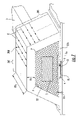
- FIG. 1 is a conceptual diagram showing the overall configuration of a magnetic storage device according to an embodiment of the present invention
- FIG. 2 is a conceptual diagram showing an enlarged storage area of the magnetic storage device of FIG. 1 ;
- FIG. 3 is an enlarged perspective view showing the internal structure of the storage area in a three-dimensional fashion
- FIG. 4 is a sectional view showing an enlarged structure of a transistor in the storage area
- FIG. 5 is a sectional view showing an enlarged structure of the ferromagnetic yoke in the storage area
- FIG. 6 is a side view showing an enlarged laminate structure of the TMR element to be arranged in the storage area
- FIG. 7 is a partially sectional perspective view schematically showing a state of magnetization of the ferromagnetic yoke in the storage area
- FIG. 8 is a partially sectional perspective view schematically showing a state of magnetization of the ferromagnetic yoke in the storage area
- FIG. 9 is a partially sectional perspective view schematically showing a state of magnetization of the ferromagnetic yoke in the storage area
- FIG. 10 is a graph showing the results of an analysis of the relationship between the magnetic path length and the write current of the magnetic storage device
- FIG. 11 is a graph showing the results of an analysis of the relationship between the magnetoresistance and the write current of the magnetic storage device
- FIG. 12 is a schematic diagram showing a theoretical field of the magnetic storage device in the absence of the TMR element
- FIG. 13 is a schematic diagram showing a theoretical field of the magnetic storage device in the presence of the TMR element
- FIG. 14 is a chart showing the results of an analysis of magnetic storage devices according to an example.
- FIG. 15 is a chart showing the results of an analysis of magnetic storage devices according to a comparative example.
- FIG. 1 is a conceptual diagram showing the overall configuration of a magnetic storage device 1 according to the embodiment of the present invention.
- the magnetic storage device 1 includes a storing unit 2 , a bit selection circuit 11 , a word selection circuit 12 , bit lines 13 and 14 , and word lines 15 and 16 .
- the storing unit 2 has a plurality of storage areas 3 which are arranged in a two-dimensional configuration (array) with m rows and n columns (m and n are integers not smaller than 2). As shown in an enlarged view of FIG.
- each storage area 3 has a TMR element 4 , a write line 5 , a read transistor 6 A, a write transistor 6 B, read lines 7 a and 7 b , a ferromagnetic yoke 20 , and the like.
- the write line 5 is laid so that it is led in from the bit line 13 .
- the storage areas 3 are provided with respective write lines 5 , ferromagnetic yokes 20 , etc. independently.
- the read lines 7 a and 7 b are arranged so as to branch out from the write line 5 .
- the TMR element 4 is interposed between one read line 7 a and the other read line 7 b.
- the TMR (magneto-resistive) element 4 has the function of changing its own resistance value based on a change in the direction of magnetization. The state of change of this resistance value is utilized to write binary data to the TMR element 4 . The direction of magnetization of this TMR element 4 is changed by an external field, which is generated by the write line 5 .
- the other end of the write line 5 laid so as to be led in from the bit line 13 , is electrically connected to the bit line 14 .
- the write transistor 6 B is switching means for controlling the conduction of a write current through the write line 5 . Its source and drain are interposed in the middle of the write line 5 . The gate is connected to the word line 16 . Consequently, a current can be passed through the word line 16 to put the write transistor 6 B into a conducting state.
- the read transistor 6 A is switching means for controlling the conduction of a read current through the read lines 7 a and 7 b . Its drain and source are interposed in the middle of the read line 7 b . The gate is connected to the word line 16 . Consequently, a current can be passed through the word line 16 to put the read transistor 6 A into a conducting state.
- the bit lines 13 and 14 are provided for each individual column of the plurality of storage areas 3 which are arranged in an array.
- the bit line 13 is connected to the write lines 5 of all the storage areas 3 that pertain to the corresponding column.
- the bit line 14 is also similarly connected to the write lines 5 of all the storage areas 3 that pertain to the corresponding column. Consequently, if a potential difference is given to between a certain pair of bit lines 13 and 14 when a write transistor 6 B is operated to permit conduction, then a write current flows through that write line 5 .
- the word lines 15 and 16 are provided for each individual row of storage areas 3 .
- the word line 16 is connected to the gates of the read transistors 6 A and the write transistors 6 B in all the storage areas 3 that pertain to the corresponding row. That is, the word line 16 serves as a line for permitting conduction of both the transistors 6 A and 6 B.
- the word line 15 is connected to read lines 7 b in all the storage areas 3 pertaining to the corresponding row. Consequently, if a potential difference is given to between a certain pair of a bit line 13 and a word line 15 when write transistors 6 A are operated to permit conduction, then a read current flows through those read lines 7 a and 7 b.
- the bit selection circuit 11 has the function of providing a positive or negative write current to the write lines 5 of the respective storage areas 3 .
- the bit selection circuit 11 includes an address decoder circuit and a current drive circuit.
- the address decoder circuit selects a predetermined column out of the array of storage areas 3 in accordance with an address designated internally or externally.
- the current drive circuit applies a positive or negative potential difference to between a pair of bit lines 13 and 14 corresponding to this predetermined column selected, and supplies a write current to the write lines 5 that are laid between the bit lines 13 and 14 in this predetermined column.
- the word selection circuit 12 includes an address decoder circuit and a current drive circuit.
- the address decoder circuit selects a predetermined row out of the array of storage areas 3 in accordance with an address designated internally or externally.
- the current drive circuit supplies predetermined voltages to the word lines 15 and 16 corresponding to this predetermined row.
- the word selection circuit 12 can be used to apply a control voltage to the word line 16 corresponding to the predetermined row so that the read transistors 6 A and the write transistors 6 B are put into a conducting state.
- bit lines 13 and 14 of the address selected by the bit selection circuit 11 During a write operation, a positive or negative potential difference is applied to between the bit lines 13 and 14 of the address selected by the bit selection circuit 11 . Accordingly, the write transistors 6 B of the address selected by the word selection circuit 12 are turned ON. This makes it possible to pass a write current through a specific storage area 3 at the intersection of the bit-side address and the word-side address. Note that the bit line 13 and the word line 15 are put to zero potential difference during a write operation so as not to pass any current through the read lines 7 .
- the bit selection circuit 11 selects a column corresponding to the address designated internally or externally using its address decoder circuit, and applies a predetermined voltage to the bit line 13 corresponding to that column.
- the word selection circuit 12 selects a row corresponding to an address by using its address decoder circuit, and applies a predetermined voltage to the word line 15 corresponding to that row. This provides a read current to between the bit line 13 and the word line 15 , and also produces a potential difference across the word line 16 to turn ON the read transistors 6 A. As a result, the read current can be passed through a specific storage area 3 at the intersection of the bit-side address and the word-side address. Note that the bit lines 13 and 14 is put to zero potential difference during a read operation so as not to pass any write current.
- FIG. 3 is a perspective view showing the state of wiring and the like of a storage area 3 in a three-dimensional fashion.
- the storage area 3 includes, roughly from below, a semiconductor layer, a wiring layer, and a magnetic material layer.
- the semiconductor layer includes a semiconductor substrate which is not shown in particular.
- Semiconductor devices such as the read transistor 6 A and the write transistor 6 B are formed thereon while maintaining the mechanical strength of the entire storage area 3 .
- the magnetic material layer at the top is primarily provided with components that are made of magnetic materials, such as the TMR element 4 and the ferromagnetic yoke 20 for applying a field to the TMR element 4 efficiently.
- the wiring layer lying in the middle is provided with the bit lines 13 and 14 , the word lines 15 and 16 , part of the write line 5 , the read line 7 b, and the like.
- the read transistor 6 A and the write transistor 6 B on the semiconductor layer are formed so that each are surrounded by an insulating area.
- the insulating area is made of an insulating material such as SiO 2 .
- An Si substrate is used as a semiconductor substrate of the transistors, for example.
- the substrate may be doped with p-type or n-type impurities.
- the read transistor 6 A is composed of a drain region 6 Aa and a source region 6 Ab of conduction type opposite to that of the semiconductor substrate 30 , as well as a gate electrode 6 Ac and the like.
- the semiconductor substrate 30 is thus interposed between the drain region 6 Aa and the source region 6 Ab, and the gate electrode 6 Ac is arranged above the semiconductor substrate 30 at a predetermined distance.
- This gate electrode 6 Ac is composed of the word line 16 .
- the drain region 6 Aa and the source region 6 Ab of the read transistor 6 A come into conduction with each other so that the read current supplied from the bit line 13 flows through the read line 7 a , the TMR element 4 , and the read line 7 b .
- the write transistor 6 B has generally the same configuration. Description thereof will thus be omitted here.
- the entire area of the wiring layer excluding the wiring such as the bit lines 13 and 14 , the word lines 15 and 16 , and the read line 7 b is occupied by an insulating area.
- this insulating area is also made of an insulating material such as SiO 2 .
- the wiring lines may be made of W or Al, for example.
- the write line 5 Adjoining the TMR element 4 , the write line 5 extends along the plane of array of the storage area 3 and is bent into an L shape within this plane. Both ends of this write line 5 are bent in a direction perpendicular to the plane to become perpendicular lines. The lower end of one of the perpendicular lines is connected to the bit line 13 . The lower end of the other perpendicular line makes an ohmic junction with the drain region 6 Ba of the write transistor 6 B through a horizontal line. A lead 14 A corresponding to each individual storage area 3 is branched out of the bit line 14 perpendicularly. Its lower end makes an ohmic junction with the source region 6 Bb of the write transistor 6 B. As a result, the write line 5 is laid to bridge a pair of bit lines 13 and 14 with the write transistor 6 B interposed therebetween.
- the read line 7 a is extended in the direction of the plane. One of its ends is electrically connected to the TMR element 4 , and the other end is connected to the write line 5 .
- One end of the read line 7 b is electrically connected to the TMR element 4 , and the other end is perpendicularly bent into a perpendicular line. The lower end of this perpendicular line makes an ohmic junction with the source region 6 Ab of the read transistor 6 A.
- a lead 15 A corresponding to each individual storage area 3 is also perpendicularly branched out of the word line 15 . Its lower end makes an ohmic junction with the drain region 6 Aa of the read transistor 6 A.
- bit line 13 and the word line 16 are electrically connected to each other through part of the write line 5 , the read line 7 a , the TMR element 4 , the read line 7 b , and the read transistor 6 A which are arranged in this order.
- the word line 16 extending in the row direction, also functions in part as the gate electrodes 6 Ac and 6 Bc of the transistors 6 A and 6 B, respectively. This is equivalent to that the word line 16 is electrically connected to the gate electrodes 6 Ac and 6 Bc of the respective transistors 6 A and 6 B.
- the magnetic material layer includes the TMR element 4 , the ferromagnetic yoke 20 , part of the write line 5 , the read line 7 a , and so on. It should be noted that the entire area of the magnetic material layer, excluding the components to be described below and other wiring, is occupied by an insulating area 24 .
- the TMR element 4 includes the following layers: 3 e ; a first magnetic layer (free layer/magnetic sensing layer) 4 A having a direction of magnetization changed by an external field; a second magnetic layer (pinned layer) 4 B having a fixed direction of magnetization; a nonmagnetic insulating layer (insulator layer) 4 C which is interposed between the first magnetic layer 4 A and the second magnetic layer 4 B; and an antiferromagnetic layer 4 D which fixes (pins) the direction of magnetization of the second magnetic layer.
- the first magnetic layer 4 A may be made of ferromagnetic materials such as Co, CoFe, NiFe, NiFeCo, and CoPt.
- the direction of magnetization of the second magnetic layer 4 B is fixed by the antiferromagnetic layer 4 D. That is, exchange coupling at the joint between the antiferromagnetic layer 4 D and the second magnetic layer 4 B stabilizes the direction of magnetization of the second magnetic layer 4 B as oriented in one direction.
- the direction of the easy axis of magnetization of the second magnetic layer 4 B is oriented along that of the first magnetic layer 4 A.
- the second magnetic layer 4 B may be made of ferromagnetic materials such as Co, CoFe, NiFe, NiFeCo, and CoPt.
- the antiferromagnetic layer 4 D may be made of such materials as IrMn, PtMn, FeMn, PtPdMn, and NiO, or any combinations of these.
- the nonmagnetic insulating layer 4 C is made of a nonmagnetic insulating material. It is interposed between the first magnetic layer 4 A and the second magnetic layer 4 B so as to produce the tunneling magneto-resistive effect (TMR). To be more specific, the nonmagnetic insulating layer 4 C characteristically varies in electric resistance depending on the relationship between the directions of magnetization of the first magnetic layer 4 A and the second magnetic layer 4 B (i.e., in parallel or antiparallel).
- the nonmagnetic insulating layer 4 C is suitably made of oxides or nitrides of such metals as Al, Zn, and Mg.
- the first magnetic layer 4 A is electrically connected to the read line 7 a .
- the antiferromagnetic layer 4 D is electrically connected to the read line 7 b .
- This configuration allows a read current to flow from the read line 7 a to the lead line 7 b through the TMR element 4 , whereby a change in the resistance of the TMR element 4 can be detected.
- the ferromagnetic yoke 20 is arranged so as to cover an area of the write line 5 adjacent to the TMR element 4 .
- the easy axis of magnetization of the first magnetic layer 4 A is oriented across the longitudinal direction of the write line 5 (i.e., across the direction of the write current).
- the TMR element 4 may be configured to have a first magnetic layer (free layer/magnetic sensing layer), a nonmagnetic insulating layer (insulator layer), a second magnetic layer, a nonmagnetic metal layer, a third magnetic layer, and an antiferromagnetic layer in this order.
- the antiferromagnetic layer fixes (pins) the direction of magnetization of the third magnetic layer.
- the nonmagnetic metal layer can be adjusted in thickness so that the direction of magnetization of the second magnetic layer becomes antiparallel with that of the third magnetic layer. This is ascribable to an exchange interaction that occurs between the second magnetic layer and the third magnetic layer.
- the ferromagnetic yoke 20 includes an element side yoke 20 A and a counter element side yoke 20 B.
- the element side yoke 20 A is arranged beside the extending write line 5 , on the side of the TMR element 4 .
- the counter element side yoke 20 B is arranged beside the write line 5 on the side opposite from the TMR element 4 .
- a pair of yoke connecting portions 20 C are arranged on both sides of the element side yoke 20 A and on both sides of the counter element side yoke 20 B so that they connect the two into a generally annular shape.
- the element side yoke 20 A is thus closer to the TMR element 4 and the counter element side yoke 20 B is farther from the TMR element 4 . It can also be said that this ferromagnetic yoke 20 itself covers part of the outer periphery of the write line 5 .
- the counter element side yoke 20 B is composed of a top area 20 T which lies above the write line 5 , and slope areas 20 S which lie on both sides of this top area 20 T, i.e., near the yoke connecting portions 20 C. It should be appreciated that the ferromagnetic yoke 20 also has the function of protecting the TMR element 4 from adversely-effecting external fields.
- the element side yoke 20 A has a gap 20 E at the center in the annular direction.
- the TMR element 4 is interposed in the gap 20 E.
- the ferromagnetic yoke 20 therefore has a general C shape with open ends 20 Ea and 20 Eb circumferentially in the middle. These open ends 20 Ea and 20 Eb are located near the sides of the TMR element 4 as extremities of the element side yoke 20 A.
- the slope areas 20 S and the yoke connecting portions 20 C guide a field that occurs in the top area 20 T toward the element side yoke 20 A (i.e., toward the TMR element 4 ).
- the internal field occurring in the top area 20 T therefore turns around through the slope areas 20 S and the yoke connecting areas 20 C, thereby forming an internal field of the opposite direction in the element side yoke 20 A.
- the counter element side yoke 20 B is shaped so that the slope areas 20 S tilt toward the element side yoke 20 A. More specifically, the angles P between the top area 20 T and the slope areas 20 S (see FIG.
- the slope areas 20 S are also given a thickness greater than that of the element side yoke 20 A.
- the top area 20 T of the counter element side yoke 20 B has a thickness TYz which is greater than the thickness BYz of the element side yoke 20 A.
- the thickness TYz is set to or above 50 nm.
- the thickness TYz has no particular ceiling as far as magnetoresistance is concerned.
- the element side yoke 20 A, thinner than the counter element side yoke 20 B, has a thickness BYz of 10 nm or above. This thickness BYz has no particular ceiling as far as magnetoresistance is concerned.
- the thickness TSz of the slope areas 20 S is set so that the counter element side yoke 20 B and the element side yoke 20 A are as continuous as possible in terms of magnetoresistance.
- the counter element side yoke 20 B has a maximum height H of, for example, 300 nm or less with respect to the TMR element 4 .
- the ferromagnetic yoke 20 has a depth (dimension in the longitudinal direction of the line) BYy of 0.45 ⁇ m to 0.8 ⁇ m. As shown in FIG.
- the width TLx of the read line 7 b is set within the range of, for example, 500 nm to 1400 nm.
- the TMR element 4 has a width MTJx of 0.2 ⁇ m to 0.8 ⁇ m. Although not shown in particular, the TMR element 4 has a depth MTJy of 0.2 ⁇ m to 1.6 ⁇ m.
- this ferromagnetic yoke 20 is preferably manufactured by depositing the slope areas 20 S and the top area 20 T in a series of processes integrally, which allows a reduction in manufacturing cost.
- the ferromagnetic yoke 20 is suitably made of ferromagnetic materials such as a metal including at least one element from among Ni, Fe, and Co.
- the magnetization X of the ferromagnetic yoke 20 preferably consists of single domains that generally coincide with the extending direction of the write line 5 . If the magnetization X includes a plurality of domains of different directions, an antiferromagnetic layer is desirably overlaid to forcefully make them into single domains. In this instance, it should be noted that the direction of magnetization B of the second magnetic layer 4 B and the direction of magnetization A of the first magnetic layer 4 A coincide with each other in the TMR element 4 . In the present embodiment, the coincidence of the directions of magnetization A and B is defined as binary data of 0 being written.
- a circumferential field F 1 occurs around the write line 5 .
- the field F 1 magnetizes the surrounding ferromagnetic yoke 20 in the direction of the magnetization X, and the ends 20 Ea and 20 Eb of the element side yoke 20 A produce a field. This field is superposed on the field F 1 to form a stronger synthetic field, which is guided toward the TMR element 4 .
- the field F 1 occurring from the write line 5 and the field induced by the magnetization X occurring in the ferromagnetic yoke 20 are combined into a strong field.
- This strong field is concentrated through the element side yoke 20 A and applied to the first magnetic layer 4 A of the TMR element 4 , thereby inverting the direction of magnetization A thereof. If the current I 1 of the write line 5 is interrupted in this state, the direction of magnetization A of the TMR element 4 continues to be inverted as shown in FIG. 8 . Since the directions of magnetization A and B are maintained as being opposite to each other, this translates into binary data of 1 being written here.
- the field F 2 occurring from the write line 5 and the field induced by the magnetization X occurring in the ferromagnetic yoke 20 are combined into a strong field.
- This strong field is concentrated through the element side yoke 20 A and applied to the first magnetic layer 4 A of the TMR element 4 , thereby inverting the direction of magnetizations.
- the direction of magnetization A of the first magnetic layer 4 A then coincides with the direction of magnetization B of the second magnetic layer 4 B again. Since the directions of magnetization A and B coincide with each other in the TMR element 4 , this translates into binary data of 0 being written again.
- a read current is passed through the read lines 7 a and 7 b to detect a change in the potential difference between the lines.
- This clarifies the resistance of the TMR element 4 to determine which binary data is recorded i.e., whether the direction of magnetization A of the first magnetic layer 4 A is in parallel or antiparallel with the direction of magnetization B of the second magnetic layer 4 B). For example, if the direction of magnetization A of the first magnetic layer 4 A coincides with the direction of magnetization B of the second magnetic layer 4 B, the resistance between the first magnetic layer 4 A and the second magnetic layer 4 B becomes relatively low due to the tunneling magneto-resistive effect (TMR) of the nonmagnetic insulating layer 4 C. Conversely, if the direction of magnetization A is opposite to the direction of magnetization B, the resistance between the first magnetic layer 4 A and the second magnetic layer 4 B becomes relatively high due to the tunneling magneto-resistive effect.
- TMR tunneling magneto-resistive effect
- L the magnetic path length of each portion
- S the sectional area
- ⁇ the magnetic permeability.
- the depth (length in the wiring direction) BYy of this ferromagnetic yoke 20 is 900 nm
- the thickness TYz of the top area 20 T is 100 nm
- the thickness BYz of the element side yoke 20 A is 20 nm
- the magnetic path length L 1 of the top area 20 T is 1200 nm
- the magnetic path length L 2 of each of the slope areas 20 S is 300 nm
- the magnetic path length L 3 of each of the portions of the counter element side yoke 20 is 350 nm.
- the total magnetic path length L is 2500 nm
- the magnetoresistance R of the entire ferromagnetic yoke 20 is 4E+10 (1/H).
- the write current I turns out to be 2.34 mA, which satisfies both the foregoing equations (1A) and (1B).
- the inventors have found that the value R of the magnetoresistance of the ferromagnetic yoke 20 is essential to magnetic storage devices 1 that have a yoke structure like the present embodiment. Specifically, they have found a scaling rule where the write current Iw decreases with the decreasing size of the ferromagnetic yoke 20 , provided that the ferromagnetic yoke 20 is arranged around the write line 5 of the magnetic storage device 1 with an appropriate adjustment in shape.
- FIG. 10 shows the results of an analysis of the relationship between the magnetic path length of the ferromagnetic yoke 20 and the write current in the magnetic storage device 1 that employs the yoke structure.
- the regression curve A that is obtained from this analysis, a magnetic path length of 1500 nm would result in zero write current. Such a situation will, in fact, not occur. That is, the scaling rule does not actually hold on an analysis that is based on the magnetic path length alone, as shown in FIG. 10 .
- the inventors then conducted an analysis on the relationship between the magnetoresistance R and the write current Iw, giving attention to the magnetoresistance R of the ferromagnetic yoke 20 .
- the results are shown in FIG. 11 .
- the analysis of the regression curve B of FIG. 11 also shows that the magnetoresistance R and the write current I can be converged to near zero.
- the scaling rule that has been considered not to hold for the magnetic storage device 1 is thus found, in fact, to hold, and this rule can be used effectively to achieve a power saving for the magnetic storage device.
- the magnetic path length of the ferromagnetic yoke 20 is Lm
- the internal field of the ferromagnetic yoke 20 is Hm
- the length of the is Hg
- the write current is Iw
- no object lies in this gap 20 E in the magnetic yoke 20 is Lx
- the field in the gap gap 20 E is Lx
- the magnetic path length of the ferromagnetic yoke 20 is Lm
- the internal field of the ferromagnetic yoke 20 is Hm
- the length of the TMR element 4 interposed in the gap 20 E of the ferromagnetic yoke 20 is Lt
- the gap width between the ferromagnetic yoke 20 and the TMR element 4 is Lg/2
- the field in the gap is Hg
- the diamagnetic field in the TMR element 4 is Hd
- the write current is Iw.
- the Maxwell equation yields the following equation (2).
- the gap 20 E (the TMR element 4 ) experiences a stronger field when the TMR element 4 lies in the magnetic circuit than when not. Consequently, the TMR element 4 placed in the magnetic circuit of the ferromagnetic yoke 20 intensifies the field due to its own presence, and can thus cause a magnetization reversal with lower currents.
- the TMR element 4 has a relative permeability that is greater than 1, and thus produces a magnetoresistance that is smaller than that of the air (the gap 20 E itself) in the magnetic circuit. This contributes the occurrence of a higher flux density (field* ⁇ 0 ) for the same current (magnetomotive force). It should be appreciated that this discussion will not hold if magnetization reversal is attempted using an external field alone without the provision of the TMR element 4 in the magnetic circuit.
- the write current Iw traces a straight line on the magnetoresistance R, and the gradient ‘a’ is equal to the field Hg acting on the TMR element 4 , multiplied by the sectional area S of the magnetic circuit and the space permeability ⁇ 0 .
- the gradient of the scaling rule becomes smaller as the field Hg acting on the TMR element 4 deceases and the sectional area S of the ferromagnetic yoke 20 (magnetic circuit) decreases.
- the intercept ‘b’ becomes smaller as the gap lengths Lg and the length Lt of the TMR element 4 decrease.
- the ferromagnetic yoke 20 is given a sectional area S of 2E+5 nm 2 or less.
- the reason for this is that the sectional area of the ferromagnetic yoke 20 , as mentioned previously, can be reduced to decrease the gradient ‘a’ effectively based on the scaling rule of the foregoing equation (5).
- this ferromagnetic yoke 20 is preferably made thicker. From the viewpoint of the scaling rule according to the present embodiment, however, it is effective to make the sectional area S of the ferromagnetic yoke 20 as small as possible.
- Reducing the width (depth) of the ferromagnetic yoke 20 is thus essential when making the ferromagnetic yoke 20 thicker. As a result, the ferromagnetic yoke becomes compact in the plane direction, thereby allowing greater integration of the magnetic storage device 1 .
- the gap widths Lg/2 between the ends of the ferroelectric yoke 20 which form the gap 20 E and the TMR element 4 which is accommodated in this gap 20 E are set to 10 nm or less. A zero gap width is ultimately preferable. Such smaller Lg can make the intercept ‘b’ on the scaling rule of the foregoing equation (5) smaller for reduced current consumption.
- a plurality of magnetic storage devices 1 were fabricated and measured for the current value Iw of the write line 5 when writing information to the TMR element 4 .
- the gap lengths (Lg/2) between the ferromagnetic yoke 20 and the TMR element 4 were set to 10 nm.
- the results are shown in FIG. 14 . Since the rest of the detailed dimensions of the magnetic storage devices 1 are shown in the chart, a description thereof will be omitted.
- the current value Iw at writing time is as extremely low as below 4 mA in any of the devices, and around 0.54 mA at the minimum. That is, the power saving of the magnetic storage devices 1 is achieved. Moreover, the write current only makes small changes in value with respect to a changing magneto resistance. These magnetic storage devices 1 having this type of yoke can thus be mass-produced with smaller variations in quality (write current value) from one product to another, which facilitates information write control.
- a plurality of magnetic storage devices was fabricated and similarly measured for the current value Iw of the write line 5 when writing information to the TMR element 4 .
- the results are shown in FIG. 15 . Since the rest of the detailed dimensions of the magnetic storage devices are shown in this chart, a description thereof will be omitted.
- the current value Iw at writing time is as high as above 10 mA in any of the devices, and around 26 mA at the maximum.
- the current makes large changes in value with respect to dimensional errors (namely, changes in magnetoresistance) of the ferromagnetic yoke 20 , which is unsuitable for mass production.
- the magnetic storage device has been described in conjunction with the embodiment thereof.
- the present invention is not limited to this embodiment, however, and various modification may also be made thereto.
- TMR elements as the magneto-resistive elements
- GMR elements which utilize the giant magneto-resistive (GMR) effect of CPP (Current Perpendicular to Plane) type.
- the GMR effect refers to a phenomenon that two ferromagnetic layers laminated with a nonmagnetic layer therebetween change in resistance in a direction perpendicular to the direction of lamination, depending on the angle formed between the directions of magnetization of the ferromagnetic layers.
- the two ferromagnetic layers show minimum resistances when the directions of magnetization of the ferromagnetic layers are in parallel with each other.
- the two ferromagnetic layer show maximum resistances when the directions of magnetization of the ferromagnetic layers are in antiparallel with each other.
- TMR elements and GMR elements both may be classified into a pseudo spin valve type in which a difference in coercivity between two ferromagnetic layers is utilized for writing and reading, and a spin valve type in which the direction of magnetization of either one of the ferromagnetic layers is fixed by exchange coupling with an antiferromagnetic layer.
- a data read on GMR elements is performed by detecting a change in the resistance of their ferromagnetic layers in a direction perpendicular to the direction of lamination.
- a data write on GMR elements is performed by inverting the direction of magnetization of either one of the ferromagnetic layers with a field caused by a write current.
- the gap made in the element side yoke refers to the final configuration of the ferromagnetic yoke 20 .
- an element side yoke 20 A of continuous shape may be formed before it is cut to make the gap. Otherwise, respective pieces of the element side yoke 20 A may be formed separately.
- magnetic storage device of the present invention is not limited to the foregoing embodiment, and various modifications may be made without departing from the gist of the present invention.
- the present invention is widely applicable to the field of recording and retaining various types of information using magneto-resistive elements.
Landscapes
- Engineering & Computer Science (AREA)
- Computer Hardware Design (AREA)
- Mram Or Spin Memory Techniques (AREA)
- Hall/Mr Elements (AREA)
- Semiconductor Memories (AREA)
Abstract
Description
Iw≦a·R+b, (1A)
where a (mA·H)=7.5E−11, and b (mA)=0.1.
Iw≦a·R+b, (1B)
where a (mA·H)=6E−11, and b (mA)=0.
rot H=j→Hm*Lm+Hg*Lx=Iw, div B=0→Hg=M/μ 0. Eq. (1)
rot H=j→Hm*Lm+Hg*Lx+(Hg−Hd)Lt=Iw, div B=0→Hg=M/μ 0. Eq. (2)
(Hg/μ s)*Lm+Hg*Lg+(Hg−Hd)Lt=Iw, and Eq. (3A)
Hgμ 0 S*(Lm/(μsμ0 S))+Hg*Lg+(Hg−Hd)Lt=Iw, Eq. (3B)
where S is the sectional area of the magnetic path.
Hgμ 0 S*R+Hg*Lg+(Hg−Hd)Lt=Iw. Eq. (4)
a·R+b=Iw, Eq. (5)
where a=Hgμ0S, and b=Hg*Lg+(Hg−Hd)Lt.
Claims (11)
Applications Claiming Priority (2)
| Application Number | Priority Date | Filing Date | Title |
|---|---|---|---|
| JP2006177122A JP5076373B2 (en) | 2006-06-27 | 2006-06-27 | Magnetic storage device and magnetic storage method |
| JP2006-177122 | 2006-06-27 |
Publications (2)
| Publication Number | Publication Date |
|---|---|
| US20080024935A1 US20080024935A1 (en) | 2008-01-31 |
| US7697323B2 true US7697323B2 (en) | 2010-04-13 |
Family
ID=38985990
Family Applications (1)
| Application Number | Title | Priority Date | Filing Date |
|---|---|---|---|
| US11/823,063 Expired - Fee Related US7697323B2 (en) | 2006-06-27 | 2007-06-25 | Magnetic storage device |
Country Status (2)
| Country | Link |
|---|---|
| US (1) | US7697323B2 (en) |
| JP (1) | JP5076373B2 (en) |
Cited By (1)
| Publication number | Priority date | Publication date | Assignee | Title |
|---|---|---|---|---|
| US20130188421A1 (en) * | 2010-09-01 | 2013-07-25 | Commissariat À L' Énergie Atomique Et Aux Énergies Alternatives | Magnetic device, and method for reading from and writing to said device |
Families Citing this family (1)
| Publication number | Priority date | Publication date | Assignee | Title |
|---|---|---|---|---|
| WO2009122519A1 (en) * | 2008-03-31 | 2009-10-08 | 株式会社 東芝 | Magnetic random access memory |
Citations (5)
| Publication number | Priority date | Publication date | Assignee | Title |
|---|---|---|---|---|
| JP2000090658A (en) | 1998-09-09 | 2000-03-31 | Sanyo Electric Co Ltd | Magnetic memory element |
| US6559511B1 (en) * | 2001-11-13 | 2003-05-06 | Motorola, Inc. | Narrow gap cladding field enhancement for low power programming of a MRAM device |
| JP3466470B2 (en) | 1998-03-18 | 2003-11-10 | 財団法人電気磁気材料研究所 | Thin film magnetoresistive element |
| US20040021189A1 (en) * | 2002-07-30 | 2004-02-05 | Hiroaki Yoda | Magnetic memory device having yoke layer, and manufacturing method thereof |
| US20050117386A1 (en) * | 2003-10-21 | 2005-06-02 | Tdk Corporation | Magnetoresistive element, magnetic memory cell, and magnetic memory device |
Family Cites Families (2)
| Publication number | Priority date | Publication date | Assignee | Title |
|---|---|---|---|---|
| JP2004235510A (en) * | 2003-01-31 | 2004-08-19 | Sony Corp | Magnetic storage device and method of manufacturing the same |
| JP2005203535A (en) * | 2004-01-15 | 2005-07-28 | Toshiba Corp | Magnetic memory |
-
2006
- 2006-06-27 JP JP2006177122A patent/JP5076373B2/en not_active Expired - Fee Related
-
2007
- 2007-06-25 US US11/823,063 patent/US7697323B2/en not_active Expired - Fee Related
Patent Citations (7)
| Publication number | Priority date | Publication date | Assignee | Title |
|---|---|---|---|---|
| JP3466470B2 (en) | 1998-03-18 | 2003-11-10 | 財団法人電気磁気材料研究所 | Thin film magnetoresistive element |
| JP2000090658A (en) | 1998-09-09 | 2000-03-31 | Sanyo Electric Co Ltd | Magnetic memory element |
| US6559511B1 (en) * | 2001-11-13 | 2003-05-06 | Motorola, Inc. | Narrow gap cladding field enhancement for low power programming of a MRAM device |
| US20040021189A1 (en) * | 2002-07-30 | 2004-02-05 | Hiroaki Yoda | Magnetic memory device having yoke layer, and manufacturing method thereof |
| JP2004128430A (en) | 2002-07-30 | 2004-04-22 | Toshiba Corp | Magnetic storage device and method of manufacturing the same |
| US20050117386A1 (en) * | 2003-10-21 | 2005-06-02 | Tdk Corporation | Magnetoresistive element, magnetic memory cell, and magnetic memory device |
| US7002840B2 (en) * | 2003-10-21 | 2006-02-21 | Tdk Corporation | Magnetoresistive element including a yoke that surrounds a conductor, magnetic memory cell and magnetic memory device including the same |
Non-Patent Citations (2)
| Title |
|---|
| Patent Abstracts of Japan Publication No. 11-274599, entitled Thin Film Magnetic Relectance Element (relevant to JP 3466470 B2). |
| Patent Abstracts of Japan Publication No. 2000-090658, entitled Magnetic Memory Element (relevant to JP 2000-90658 A). |
Cited By (2)
| Publication number | Priority date | Publication date | Assignee | Title |
|---|---|---|---|---|
| US20130188421A1 (en) * | 2010-09-01 | 2013-07-25 | Commissariat À L' Énergie Atomique Et Aux Énergies Alternatives | Magnetic device, and method for reading from and writing to said device |
| US8811073B2 (en) * | 2010-09-01 | 2014-08-19 | Commissariat A L'energie Atomique Et Aux Energies Alternatives | Magnetic device, and method for reading from and writing to said device |
Also Published As
| Publication number | Publication date |
|---|---|
| JP5076373B2 (en) | 2012-11-21 |
| JP2008010511A (en) | 2008-01-17 |
| US20080024935A1 (en) | 2008-01-31 |
Similar Documents
| Publication | Publication Date | Title |
|---|---|---|
| US8040724B2 (en) | Magnetic domain wall random access memory | |
| JP2010114143A (en) | Semiconductor memory device, and method of manufacturing the same | |
| JPWO2007119446A1 (en) | MRAM and data read / write method of MRAM | |
| US7613033B2 (en) | Magnetic storage device | |
| US7016221B2 (en) | Magnetoresistive effect element, magnetic memory device and method of fabricating the same | |
| JP2008171862A (en) | Magnetoresistive element and MRAM | |
| JP2009164390A (en) | Magnetic recording device | |
| US7697323B2 (en) | Magnetic storage device | |
| US7613034B2 (en) | Magnetic memory and method for reading-writing information from-to magnetic storage element | |
| JP5445029B2 (en) | Magnetoresistive element and domain wall random access memory | |
| JP2004303837A (en) | Magnetic storage cell, magnetic memory device, and its manufacturing method | |
| JP4667763B2 (en) | Magnetic memory element and semiconductor device | |
| US7649766B2 (en) | Magnetic storage device | |
| JP2002353418A (en) | Magnetoresistive element and magnetic memory device | |
| JP2007059865A (en) | Magnetic storage | |
| JP2004296858A (en) | Magnetic storage element and magnetic storage device | |
| US7453721B2 (en) | Magnetic memory | |
| US7903453B2 (en) | Magnetic memory | |
| JP4720081B2 (en) | Magnetic memory | |
| JP4952053B2 (en) | Magnetic storage | |
| US20060056232A1 (en) | Magnetic memory and manufacturing method thereof | |
| JP2006156893A (en) | Magnetic memory | |
| JP2008235659A (en) | Method for manufacturing yoke-type magnetic storage device, and yoke-type magnetic storage device | |
| JP2006128220A (en) | Magnetic memory | |
| US20060062075A1 (en) | Magnetic memory |
Legal Events
| Date | Code | Title | Description |
|---|---|---|---|
| AS | Assignment |
Owner name: TDK CORPORATION, JAPAN Free format text: ASSIGNMENT OF ASSIGNORS INTEREST;ASSIGNORS:TAGAMI, KATSUMICHI;KOGA, KEIJI;OIKAWA, TOHRU;REEL/FRAME:019808/0001 Effective date: 20070611 Owner name: TDK CORPORATION,JAPAN Free format text: ASSIGNMENT OF ASSIGNORS INTEREST;ASSIGNORS:TAGAMI, KATSUMICHI;KOGA, KEIJI;OIKAWA, TOHRU;REEL/FRAME:019808/0001 Effective date: 20070611 |
|
| FEPP | Fee payment procedure |
Free format text: PAYOR NUMBER ASSIGNED (ORIGINAL EVENT CODE: ASPN); ENTITY STATUS OF PATENT OWNER: LARGE ENTITY |
|
| REMI | Maintenance fee reminder mailed | ||
| LAPS | Lapse for failure to pay maintenance fees | ||
| STCH | Information on status: patent discontinuation |
Free format text: PATENT EXPIRED DUE TO NONPAYMENT OF MAINTENANCE FEES UNDER 37 CFR 1.362 |
|
| STCH | Information on status: patent discontinuation |
Free format text: PATENT EXPIRED DUE TO NONPAYMENT OF MAINTENANCE FEES UNDER 37 CFR 1.362 |
|
| FP | Lapsed due to failure to pay maintenance fee |
Effective date: 20140413 |