US7693930B2 - Asynchronous full adder, asynchronous microprocessor and electronic apparatus - Google Patents
Asynchronous full adder, asynchronous microprocessor and electronic apparatus Download PDFInfo
- Publication number
- US7693930B2 US7693930B2 US11/060,764 US6076405A US7693930B2 US 7693930 B2 US7693930 B2 US 7693930B2 US 6076405 A US6076405 A US 6076405A US 7693930 B2 US7693930 B2 US 7693930B2
- Authority
- US
- United States
- Prior art keywords
- asynchronous
- dual
- mosfets
- rail
- output
- Prior art date
- Legal status (The legal status is an assumption and is not a legal conclusion. Google has not performed a legal analysis and makes no representation as to the accuracy of the status listed.)
- Expired - Fee Related, expires
Links
- 238000001514 detection method Methods 0.000 claims description 7
- 230000005669 field effect Effects 0.000 claims 1
- 239000004065 semiconductor Substances 0.000 claims 1
- 238000000034 method Methods 0.000 description 36
- 230000008569 process Effects 0.000 description 35
- 230000001360 synchronised effect Effects 0.000 description 6
- 238000004088 simulation Methods 0.000 description 3
- 230000008901 benefit Effects 0.000 description 2
- 238000005516 engineering process Methods 0.000 description 2
- 230000015572 biosynthetic process Effects 0.000 description 1
- 230000000903 blocking effect Effects 0.000 description 1
- 230000001413 cellular effect Effects 0.000 description 1
- 230000000295 complement effect Effects 0.000 description 1
- 238000012938 design process Methods 0.000 description 1
- 230000000694 effects Effects 0.000 description 1
- 230000002708 enhancing effect Effects 0.000 description 1
- 239000011521 glass Substances 0.000 description 1
- 230000036541 health Effects 0.000 description 1
- 230000004044 response Effects 0.000 description 1
- 230000000630 rising effect Effects 0.000 description 1
- 238000004513 sizing Methods 0.000 description 1
- 235000013599 spices Nutrition 0.000 description 1
- 238000003786 synthesis reaction Methods 0.000 description 1
- 230000007704 transition Effects 0.000 description 1
Images


Classifications
-
- G—PHYSICS
- G06—COMPUTING; CALCULATING OR COUNTING
- G06F—ELECTRIC DIGITAL DATA PROCESSING
- G06F7/00—Methods or arrangements for processing data by operating upon the order or content of the data handled
- G06F7/38—Methods or arrangements for performing computations using exclusively denominational number representation, e.g. using binary, ternary, decimal representation
- G06F7/48—Methods or arrangements for performing computations using exclusively denominational number representation, e.g. using binary, ternary, decimal representation using non-contact-making devices, e.g. tube, solid state device; using unspecified devices
- G06F7/50—Adding; Subtracting
- G06F7/501—Half or full adders, i.e. basic adder cells for one denomination
-
- G—PHYSICS
- G06—COMPUTING; CALCULATING OR COUNTING
- G06F—ELECTRIC DIGITAL DATA PROCESSING
- G06F2207/00—Indexing scheme relating to methods or arrangements for processing data by operating upon the order or content of the data handled
- G06F2207/38—Indexing scheme relating to groups G06F7/38 - G06F7/575
- G06F2207/3804—Details
- G06F2207/386—Special constructional features
- G06F2207/3864—Clockless, i.e. asynchronous operation used as a design principle
Definitions
- Exemplary embodiments of the present invention relate to an asynchronous full adder, and more particularly to an enhanced technique thereof to employ a dual-rail scheme for the datapath, including arithmetic-logic unit (ALU), of asynchronous microprocessors.
- ALU arithmetic-logic unit
- An ALU of a microprocessor that performs arithmetic and logic operation, such as addition, subtraction, logical OR and AND, includes a full adder, an accumulator register, a flag resister, etc.
- ALUs are designed in optimum schemes that are employed with regard to the applications, performance, power consumption, chip area and other factors.
- the related art includes a ripple-carry adder and a carry-lookahead adder.
- the ripple-carry adder is slightly inferior to the carry-lookahead adder in operation speed.
- the ripple-carry adder leads to a smaller chip area, and therefore is most typically used in microprocessor design.
- the datapath circuit including an adder is driven by global clock in synchronous design.
- the operation speed of the microprocessor solely depends on the delay of the critical path.
- the ripple-carry adder which leads to a smaller chip area, has an advantage over carry-lookahead adders.
- control part of asynchronous designs is to be based on the dual-rail encoding scheme, while the datapath is designed preferably based on the bundle-data single-rail scheme.
- the datapath, including an adder, that has been prepared for a synchronous design can be reused for the asynchronous design, taking the advantages of less labor/time and small chip area.
- the condition for the stable operation is that the KPG signals get stable at the time when the carry output unit receives dual-rail encoded signals from the carry input unit.
- the KPG unit at each stage generates KPG signals based on the value of two addends input to the ALU. Only the superior system of the ALU can arrange for the KPG signals to be generated according to all the addends prior to the time when dual-rail signals from the control arrive. Thus, the related art has not completely accomplished a dual-rail scheme.
- exemplary embodiments of the present invention address or realize asynchronous design in which dual-rail encoding is totally employed, not only for the control, but also for the datapath including ALU. Furthermore, exemplary embodiments of the present invention reduce labor and time for the datapath design, enhance the portability of IP of asynchronous processes, and absorb deviation in switching delay due to deviation in threshold voltage of transistors so as to enhance the robustness. Also, exemplary embodiments of the present invention address or achieve higher performance with less delay in average case design, and address or solve the clock-skew problem in synchronous design.
- an asynchronous adder of exemplary embodiments of the present invention includes a combinational circuit to perform full addition with two addends, and a carry-in that are dual-rail encoded, and to output a sum and a carry output that are dual-rail encoded.
- This configuration addresses or realizes asynchronous designs in which dual-rail encoding is employed, not only for the control part, but also for the datapath part including the ALU.
- the asynchronous adder of exemplary embodiments of the present invention preferably further include a detection device to detect Null of the input values. Furthermore, the combinational circuit preferably performs full addition, based on the input values if values other than Null are input.
- the combinational circuit preferably includes: an N-ch MOSFET network including a plurality of columns of cascaded N-ch MOSFETs between a node and ground; a precharge device to precharge the node if the detection device detects Null of input values; a connecting device to connect input signals to gate terminals of the N-ch MOSFETs based on a truth table which specifies a combinational logic required to compute an output signal from input signals; and a buffer to drive the node to a voltage of the output value.
- drain terminals of the N-ch MOSFETs at uppermost stages of all columns are preferably connected to the node, and source terminals of the N-ch MOSFETs at lowermost stages of all columns are preferably connected to the ground. Since the input values are delimited by Nulls, the node shall be precharged at the timing when Nulls are detected.
- the asynchronous adder of exemplary embodiments of the present invention may further include a device to, if values other than Null are input, control so that the precharge device does not precharge the node during a period when all N-ch MOSFETs of any column of the N-ch MOSFET network are ON. This configuration avoids a wasteful current flowing through the precharge device and the N-ch MOSFET network.
- the asynchronous adder of exemplary embodiments of the present invention may further include dual-rail decoders that decode dual-rail encoded input values.
- the asynchronous microprocessor of exemplary embodiments of the present invention includes the asynchronous adder of exemplary embodiments of the present invention.
- An asynchronous microprocessor can be achieved, in which dual-rail encoding scheme is totally employed, not only for the control part, but also for the datapath part including the ALU.
- the electronic apparatus of exemplary embodiments of the present invention includes the asynchronous microprocessor of exemplary embodiments of the present invention.
- a high performance electronic apparatus utilizing the advantageous features of the asynchronous microprocessor of exemplary embodiments of the present invention can be provided.
- FIG. 1 is a schematic of an asynchronous adder of a first exemplary embodiment
- FIG. 2 is a schematic of a dual-rail encoding scheme
- FIG. 3 is a schematic of a precharge signal generator
- FIG. 4 is a schematic of a combinational circuit of the first exemplary embodiment
- FIG. 5 is a truth table for input and output signals
- FIG. 6 is a schematic of a dual-rail decoder
- FIG. 7 is a schematic of the dual-rail decoder
- FIG. 8 is a schematic of a 4-bit full adder
- FIG. 9 is a schematic of four-phase handshaking
- FIG. 10 is a schematic of four-phase handshaking
- FIG. 11 is a schematic of a combinational circuit of a second exemplary embodiment.
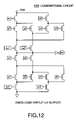
- FIG. 12 is a schematic of a combinational circuit of a third exemplary embodiment.
- An asynchronous adder of the present exemplary embodiment includes a combinational circuit.
- the combinational circuit performs full addition with, as input values, addends X, Y and a carry-in C in in that are dual-rail encoded, and outputs a sum Z and a carry C out that are dual-rail encoded.
- This configuration addresses or realizes asynchronous designs in which dual-rail encoding is employed, not only for the control part, but also for the datapath part including the ALU.
- FIG. 1 is a schematic showing the input/output relationship of an asynchronous adder 10 of a first exemplary embodiment.
- the asynchronous adder 10 is a 1-bit full adder that receives the dual-rail encoded addends X, Y and carry-in C in to perform full addition, and outputs the dual-rail encoded sum Z and carry C out .
- the addends X, Y and carry-in C in are encoded to ⁇ x — 1, x — 0 ⁇ , ⁇ y — 1, y — 0 ⁇ , ⁇ c in — 1, c in — 0 ⁇ according to the dual-rail encoding scheme.
- the sum Z and carry C out are also encoded to ⁇ z — 1, z — 0 ⁇ and ⁇ c out — 1, c out — 0 ⁇ respectively.
- FIG. 2 is a table showing a dual-rail encoding scheme. According to FIG. 2 , “0”, “1” and “Null” are converted to ⁇ 0, 1 ⁇ , ⁇ 1, 0 ⁇ and ⁇ 0, 0 ⁇ , respectively. The data “0” and “1” are fed to the asynchronous adder 10 while “Null” codes are interposed between the data “0” and “1” as delimiters.
- FIG. 6 is a schematic showing the input/output relationship of a dual-rail decoder 20 .
- FIG. 7 is a schematic showing the specific circuit arrangement of the dual-rail decoder 20 .
- ⁇ x — 1, x — 0 ⁇ is converted to ⁇ x1, x0 ⁇ by dual-rail decoding.
- FIG. 3 is a schematic showing a precharge signal generator, serving as a detection device to detect Null of the inputs values X, Y and C in . If all dual-rail encoded inputs X, Y and C in are “Null”, i.e., all of x1, x0, y1, y0, c in 1 and c in 0 are “0”, the precharge signal generator 40 switches the logic level of a precharge_signal to Low.
- the precharge_signal gives timing of precharging an N-ch MOSFET network, described below. Just for conventions here, the symbol A_stands for the logical NOT of A, i.e., the low level is TRUE.
- the asynchronous adder 10 includes a combinational circuit to perform full addition based on the dual-rail encoded input values X, Y and C in , and output the dual-rail encoded sum Z and carry C out .
- This combinational circuit is configured based on a truth table satisfying equations (1) and (2).
- FIG. 5 is a truth table obtained by equations (1) and (2) and showing all combinations between input and output.
- FIG. 4 is a schematic showing one example of a combinational circuit 30 to compute z1.
- the combinational circuit 30 includes an N-ch MOSFET network 31 that has a plurality of columns of cascaded N-ch MOSFETs between a node 32 and the ground, a P-ch MOSFET 33 as a precharge device to precharge the node 32 when all input values X, Y and C in are “Null”, and an inverter 34 that inverting-outputs the voltage of the node 32 .
- the output value of the inverter 34 is z1.
- the N-ch MOSFET network 31 includes twelve N-ch MOSFETs 41 through 52 of three stages and four columns.
- the drain terminals of the N-ch MOSFETs 41 , 44 , 47 and 50 at the uppermost stages of all columns are connected to the node 32 .
- the source terminals of the N-ch MOSFETs 43 , 46 , 49 and 52 at the lowermost stages are grounded.
- Each gate terminal of the N-ch MOSFETs 41 through 52 is connected to an input signal line (x1, x0, y1, y0, c in 1 and c in 0) based on the truth table for input and output signals.
- the number of columns in the N-ch MOSFET network 31 (four in this exemplary embodiment) is the same as the number of combinations of input values with which z1 is set to High (four in this exemplary embodiment).
- Combinational circuits to compute z0, c out 1 and c out 0 can also be configured based on the truth table ( FIG. 5 ), similarly as above illustrated.
- the above described precharge signal generator 40 switches the logic level of a precharge_signal to Low. Then, the P-ch MOSFET 33 is turned ON so as to precharge the node 32 to a logic level High with a power supply Vdd. At that time, the logic level of z1 is Low. When any of input values X, Y and C in takes “0” or “1”, the logic level of a precharge_signal is High, turning the P-ch MOSFET 33 OFF. At that time, signals at a Low or High level corresponding to “0” or “1” are input to the gate terminals of the N-ch MOSFETs 41 through 52 . If all cascaded N-ch MOSFETs of any column are turned ON, the logic level of the node 32 is switched from High to Low, and thus the logic level of z1 is switched from Low to High.
- the P-ch MOSFET 33 is turned OFF prior to turning ON the N-ch MOSFETs 41 through 52 to discourage or avoid a current flowing through the power supply Vdd to the ground.
- the N-ch MOSFET network 31 for convenience, twelve N-ch MOSFETs 41 through 52 are arranged in order to clearly show the correspondence between the arrangement of the N-ch MOSFETs 41 through 52 and the truth table ( FIG. 5 ). If necessary, the connection relationship in the N-ch MOSFETs 41 through 52 may be enhanced or optimized to reduce the number of transistors.
- the N-ch MOSFETs 43 and 46 can be replaced by a single N-ch MOSFET.
- a combinational circuit may be configured so that c out 1 is “1” irrespective of whether c in 1 is “1” or “0” when x1 and y1 are “1”.
- the combinational circuit 30 may employ a P-ch MOSFET network made up of plural P-ch MOSFETs instead of the N-ch MOSFET network 31 .
- FIG. 8 is a schematic of a 4-bit asynchronous full adder 90 .
- the asynchronous adder 90 includes four 1-bit full adders 91 through 94 .
- the carry from a lower-order bit is fed to the carry-in of the upper-order bit.
- the two 4-bit addends, 4-bit sum, 1-bit carry-in and 1-bit carry are represented as X[3:0], Y[3:0], Z[3:0], C in and C out , respectively.
- FIG. 9 is a schematic of a four-phase handshaking in the asynchronous adder 90 .
- the asynchronous adder 90 is connected to each of processes A, B, C and Op through a 4-bit channel, as shown in the drawing.
- the process A has an active output port.
- the process A outputs a 4-bit addend X to the asynchronous adder 90 and waits for an acknowledge signal from the process C.
- the process B has an active output port.
- the process B outputs another 4-bit addend Y to the asynchronous adder 90 and waits for an acknowledge signal from the process C.
- the process Op controls whether the asynchronous adder 90 performs addition or subtraction, and so forth.
- the process Op communicates with the process B so as to have an effect on the output value from the process B.
- the subtracted value is logically inverted simply by an inverter (not shown) or the like. Subtraction can be performed by adding the 2's complement as above. It is not necessary that the request signals from the processes A, B and Op are simultaneously fed to the asynchronous adder 90 .
- the process C has a passive input port to receive an output from the asynchronous adder 90 . Upon the receiving the sum Z from the asynchronous adder 90 , the process C outputs acknowledge signals to the processes A, B and Op.
- FIG. 10 is a schematic showing handshaking among the processes.
- the symbol ⁇ T adder indicates the delay of the asynchronous adder 90 .
- the process Op first outputs the 1-bit carry-in C in .
- the addends X and Y are output from the process A and B respectively.
- the asynchronous adder 90 outputs the sum Z to the process C when the time of ⁇ T adder elapses after the asynchronous adder 90 has received all of the addends X, Y and carry-in C in .
- the sum Z is input to the process C as one request, i.e., Req_A&B&Op, obtained by merging three request signals from the processes A, B and Op (X as Req_A, Y as Req_B and C in as Req_Op).
- the process C outputs an acknowledge signal in response to the request. That is, the process C switches Ack_C to High.
- the acknowledge signal is input to the processes A, B and Op.
- Each of the processes A, B and Op receives the acknowledge signal and negates the respective request signal, i.e., outputs “Null”.
- the asynchronous adder 90 outputs “Null” to the sum output Z after a certain computation delay.
- the process C switches the acknowledge signal to Low, responding to that the sum output Z as Req_A&B&Op is “Null”.
- An asynchronous adder of the present exemplary embodiment may be imported easily and surely by “cut open” of channels between processes. “Cut open” may take place after logic synthesis of the control part, which is temporarily separated from and afterward connected with the data part.
- FIG. 11 is a schematic showing a configuration example of a combinational circuit 80 , which is another example of a combinational circuit, to perform computing z1.
- the same numerals as those in FIG. 4 indicate the same elements and so forth, and detailed description for the elements will be omitted.
- the combinational circuit 80 further includes, in addition to the configuration of the above combinational circuit 30 , a Null detector 70 for detecting Null of an input signal and N-ch MOSFETs 71 through 74 to time the N-ch MOSFET network 31 to be turned ON.
- the Null detector 70 detects Null of the input signal so as to make the precharge_signal low to turn ON the P-ch MOSFET 33 .
- the Null detector 70 feeds control signals to gate terminals of the N-ch MOSFETs 71 through 74 so as to turn ON the N-ch MOSFETs 71 through 74 .
- timing the N-ch MOSFETs 71 through 74 to turn ON can discourage or prevent a wasteful current that flows from the power supply Vdd to the ground when the P-ch MOSFET 33 and the N-ch MOSFET network 31 are simultaneously turned ON.
- FIG. 12 is a schematic showing the configuration of a combinational circuit 100 of the present exemplary embodiment.
- FIG. 12 shows an example in which CMOS logic circuits constitute a combinational circuit to generate z — 1 output of the dual-rail encoded sum Z.
- the combinational circuit 100 is configured so that the input/output relationship of the asynchronous adder 10 satisfies equations (1) and (2).
- the combinational circuit for full addition is made up of CMOS logic, which is preferably arranged to reduce or suppress glitches caused by input transitions, even without a Null detection circuit. Since glitches cause incorrect operation of circuits, it is necessary to suppress glitches.
- An asynchronous microprocessor of the present exemplary embodiment includes any of the asynchronous adders disclosed in the first through third exemplary embodiments.
- An asynchronous microprocessor is a microprocessor in which optimally grained functional circuits (processes) locally cooperate with each other actively or passively to perform distributed processing without using global clock.
- various operations such as “instruction fetch”, “decode”, “execute” and “write back” are performed in sync with global clock, and therefore clock delay, clock skew, clock jitter and so forth become problematic in enhancing the speed of circuit operation.
- an asynchronous microprocessor does not involve such problems since optimally grained and self-timed functional circuits communicate by handshaking and cooperate with each other actively or passively in an event-driven fashion.
- optimally grained functional circuits are driven by events to operate only when either active or passive operation is determined in semantics to take place.
- each optimally grained functional circuit can operate in parallel independently of other functional circuits, and need not wait for the completion of operations by the other functional circuits. Once the condition for a functional circuits is satisfied to go, it remains on standby for quick service. All the processes are blocking under the condition.
- An electronic apparatus of the present exemplary embodiment includes the asynchronous microprocessor of the fourth exemplary embodiment.
- the term electronic apparatus refers to typical equipment having a circuit board and other elements, and exerts a certain function. The structure thereof is not limited particularly. Examples of such an electronic apparatus includes a battery-driven portable apparatus, a sheet computer, an electronic paper, a wearable computer, an IC card, a smart card, a cellular phone, a video camera, a personal computer, a head mounted display, a projector of rear or front type, a wearable health management apparatus, a wearable toy, a pervasive wireless sensor, radio frequency identification (RFID), an attached thermometer, a facsimile device with a display function, a portable TV, a personal digital assistant (PDA), an electronic notebook, a sheet calculator, an electronic signboard, an advertisement display, a wireless tag with a display function, a system on panel (SOP) and a system on glass (SOG), for example.
- RFID radio frequency identification
- PDA
Abstract
Description
Z=X⊕Y⊕Cin (1)
C out =X·Y+Y·C in +C in ·X (2)
Claims (6)
Applications Claiming Priority (4)
| Application Number | Priority Date | Filing Date | Title |
|---|---|---|---|
| JP2004-086465 | 2004-03-24 | ||
| JP2004086465 | 2004-03-24 | ||
| JP2004277309A JP3912545B2 (en) | 2004-03-24 | 2004-09-24 | Asynchronous adder, asynchronous processor, and electronic device |
| JP2004-277309 | 2004-09-24 |
Publications (2)
| Publication Number | Publication Date |
|---|---|
| US20050216546A1 US20050216546A1 (en) | 2005-09-29 |
| US7693930B2 true US7693930B2 (en) | 2010-04-06 |
Family
ID=34991430
Family Applications (1)
| Application Number | Title | Priority Date | Filing Date |
|---|---|---|---|
| US11/060,764 Expired - Fee Related US7693930B2 (en) | 2004-03-24 | 2005-02-18 | Asynchronous full adder, asynchronous microprocessor and electronic apparatus |
Country Status (2)
| Country | Link |
|---|---|
| US (1) | US7693930B2 (en) |
| JP (1) | JP3912545B2 (en) |
Cited By (4)
| Publication number | Priority date | Publication date | Assignee | Title |
|---|---|---|---|---|
| US20070030031A1 (en) * | 2005-08-08 | 2007-02-08 | Infineon Technologies Ag | Circuit and method for calculating a logic combination of two encrypted input operands |
| US20100329446A1 (en) * | 2005-08-08 | 2010-12-30 | Infineon Technologies Ag | Logic circuit and method for calculating an encrypted result operand |
| US20110279242A1 (en) * | 2010-05-14 | 2011-11-17 | Mark Krawczewicz | Batteryless stored value card with display |
| US9524270B2 (en) | 2010-04-30 | 2016-12-20 | Cornell University | Operand-optimized asynchronous floating-point units and method of use thereof |
Families Citing this family (5)
| Publication number | Priority date | Publication date | Assignee | Title |
|---|---|---|---|---|
| JP4147423B2 (en) * | 2004-11-12 | 2008-09-10 | セイコーエプソン株式会社 | Arbitrary precision computing unit, arbitrary precision computing method, and electronic device |
| US20070189578A1 (en) * | 2005-05-25 | 2007-08-16 | Macrovision Corporation | Computer-implemented method and system for perceptual cryptography in file-sharing environments |
| CN102521620B (en) * | 2011-11-25 | 2013-09-25 | 山东泰宝防伪技术产品有限公司 | Anti-fake label detection device of coiled tape label, and method for the same |
| JP5958138B2 (en) * | 2012-07-19 | 2016-07-27 | セイコーエプソン株式会社 | Asynchronous full adder, asynchronous correlation arithmetic circuit, arithmetic device and correlation arithmetic device |
| WO2015116812A1 (en) | 2014-01-30 | 2015-08-06 | Express Imaging Systems, Llc | Ambient light control in solid state lamps and luminaires |
Citations (12)
| Publication number | Priority date | Publication date | Assignee | Title |
|---|---|---|---|---|
| US3290511A (en) | 1960-08-19 | 1966-12-06 | Sperry Rand Corp | High speed asynchronous computer |
| US5208490A (en) | 1991-04-12 | 1993-05-04 | Hewlett-Packard Company | Functionally complete family of self-timed dynamic logic circuits |
| JPH05233214A (en) | 1991-04-12 | 1993-09-10 | Hewlett Packard Co <Hp> | Universal pipeline latch for rodent trap logic circuit |
| JPH06152386A (en) | 1992-05-19 | 1994-05-31 | Hewlett Packard Co <Hp> | Automatic time-adjusting clock system for automatic time-adjusting dynamic logic circuit |
| US5329176A (en) | 1991-04-12 | 1994-07-12 | Hewlett-Packard Company | Self-timed clocking system and method for self-timed dynamic logic circuits |
| JPH06282415A (en) | 1993-02-03 | 1994-10-07 | Hewlett Packard Co <Hp> | Method for vector logic |
| US5636157A (en) * | 1994-10-03 | 1997-06-03 | International Business Machines Corporation | Modular 64-bit integer adder |
| US5752070A (en) | 1990-03-19 | 1998-05-12 | California Institute Of Technology | Asynchronous processors |
| US6031390A (en) * | 1997-12-16 | 2000-02-29 | Theseus Logic, Inc. | Asynchronous registers with embedded acknowledge collection |
| US6152613A (en) | 1994-07-08 | 2000-11-28 | California Institute Of Technology | Circuit implementations for asynchronous processors |
| US6466960B1 (en) * | 1999-05-13 | 2002-10-15 | Hewlett-Packard Company | Method and apparatus for performing a sum-and-compare operation |
| US6785703B2 (en) * | 2001-05-24 | 2004-08-31 | International Business Machines Corporation | Simultaneous dual rail static carry-save-adder circuit using silicon on insulator technology |
-
2004
- 2004-09-24 JP JP2004277309A patent/JP3912545B2/en not_active Expired - Fee Related
-
2005
- 2005-02-18 US US11/060,764 patent/US7693930B2/en not_active Expired - Fee Related
Patent Citations (13)
| Publication number | Priority date | Publication date | Assignee | Title |
|---|---|---|---|---|
| US3290511A (en) | 1960-08-19 | 1966-12-06 | Sperry Rand Corp | High speed asynchronous computer |
| US5752070A (en) | 1990-03-19 | 1998-05-12 | California Institute Of Technology | Asynchronous processors |
| US5392423A (en) | 1991-04-12 | 1995-02-21 | Hewlett-Packard Company | Universal pipeline latch for mousetrap logic circuits |
| US5208490A (en) | 1991-04-12 | 1993-05-04 | Hewlett-Packard Company | Functionally complete family of self-timed dynamic logic circuits |
| JPH05233214A (en) | 1991-04-12 | 1993-09-10 | Hewlett Packard Co <Hp> | Universal pipeline latch for rodent trap logic circuit |
| US5329176A (en) | 1991-04-12 | 1994-07-12 | Hewlett-Packard Company | Self-timed clocking system and method for self-timed dynamic logic circuits |
| JPH06152386A (en) | 1992-05-19 | 1994-05-31 | Hewlett Packard Co <Hp> | Automatic time-adjusting clock system for automatic time-adjusting dynamic logic circuit |
| JPH06282415A (en) | 1993-02-03 | 1994-10-07 | Hewlett Packard Co <Hp> | Method for vector logic |
| US6152613A (en) | 1994-07-08 | 2000-11-28 | California Institute Of Technology | Circuit implementations for asynchronous processors |
| US5636157A (en) * | 1994-10-03 | 1997-06-03 | International Business Machines Corporation | Modular 64-bit integer adder |
| US6031390A (en) * | 1997-12-16 | 2000-02-29 | Theseus Logic, Inc. | Asynchronous registers with embedded acknowledge collection |
| US6466960B1 (en) * | 1999-05-13 | 2002-10-15 | Hewlett-Packard Company | Method and apparatus for performing a sum-and-compare operation |
| US6785703B2 (en) * | 2001-05-24 | 2004-08-31 | International Business Machines Corporation | Simultaneous dual rail static carry-save-adder circuit using silicon on insulator technology |
Non-Patent Citations (1)
| Title |
|---|
| Renaudin et al.,"The Design of Fast Asynchronous Adder Structures and Their Implementation Using D.C.V.S. Logic", Circuits and Systems, 1994. ISCAS '94., 1994 IEEE International Symposium, pp. 291-294. * |
Cited By (7)
| Publication number | Priority date | Publication date | Assignee | Title |
|---|---|---|---|---|
| US20070030031A1 (en) * | 2005-08-08 | 2007-02-08 | Infineon Technologies Ag | Circuit and method for calculating a logic combination of two encrypted input operands |
| US20100329446A1 (en) * | 2005-08-08 | 2010-12-30 | Infineon Technologies Ag | Logic circuit and method for calculating an encrypted result operand |
| US7876893B2 (en) | 2005-08-08 | 2011-01-25 | Infineon Technologies Ag | Logic circuit and method for calculating an encrypted result operand |
| US7881465B2 (en) * | 2005-08-08 | 2011-02-01 | Infineon Technologies Ag | Circuit and method for calculating a logic combination of two encrypted input operands |
| US9524270B2 (en) | 2010-04-30 | 2016-12-20 | Cornell University | Operand-optimized asynchronous floating-point units and method of use thereof |
| US20110279242A1 (en) * | 2010-05-14 | 2011-11-17 | Mark Krawczewicz | Batteryless stored value card with display |
| US9122964B2 (en) * | 2010-05-14 | 2015-09-01 | Mark Krawczewicz | Batteryless stored value card with display |
Also Published As
| Publication number | Publication date |
|---|---|
| US20050216546A1 (en) | 2005-09-29 |
| JP3912545B2 (en) | 2007-05-09 |
| JP2005310097A (en) | 2005-11-04 |
Similar Documents
| Publication | Publication Date | Title |
|---|---|---|
| US7693930B2 (en) | Asynchronous full adder, asynchronous microprocessor and electronic apparatus | |
| US5420808A (en) | Circuitry and method for reducing power consumption within an electronic circuit | |
| US6202163B1 (en) | Data processing circuit with gating of clocking signals to various elements of the circuit | |
| US9448811B2 (en) | Microprocessor device, and method of managing reset events therefor | |
| US20070204138A1 (en) | Device, system and method of tracking data validity | |
| US20090070609A1 (en) | Power throttling apparatus | |
| US6584485B1 (en) | 4 to 2 adder | |
| US20050241005A1 (en) | Data processing apparatus and method for operating a dual rail circuit component | |
| US20120151191A1 (en) | Reducing power consumption in multi-precision floating point multipliers | |
| Kwon et al. | Design trade-offs in floating-point unit implementation for embedded and processing-in-memory systems | |
| US7188134B2 (en) | High-performance adder | |
| CN101960422A (en) | A dual function adder for computing a hardware prefetch address and an arithmetic operation value | |
| US20040220994A1 (en) | Low power adder circuit utilizing both static and dynamic logic | |
| US20050116740A1 (en) | Data processing circuit and method for transmitting data | |
| US6631393B1 (en) | Method and apparatus for speculative addition using a limited carry | |
| EP3067819B1 (en) | Logic compound register system and method for resisting energy analysis attacks | |
| US7325024B2 (en) | Adder circuit with sense-amplifier multiplexer front-end | |
| US7284029B2 (en) | 4-to-2 carry save adder using limited switching dynamic logic | |
| US9116701B2 (en) | Memory unit, information processing device, and method | |
| Moon et al. | An area-efficient standard-cell floating-point unit design for a processing-in-memory system | |
| US6144228A (en) | Generalized push-pull cascode logic technique | |
| Bartlett et al. | A self-timed multiplier using conditional evaluation | |
| Boppana et al. | Low-power and high speed CPL-CSA adder | |
| Obridko et al. | Low energy asynchronous adders | |
| Corsonello et al. | A new high performance circuit for statistical carry lookahead addition |
Legal Events
| Date | Code | Title | Description |
|---|---|---|---|
| AS | Assignment |
Owner name: SEIKO EPSON CORPORATION, JAPAN Free format text: ASSIGNMENT OF ASSIGNORS INTEREST;ASSIGNOR:KARAKI, NOBUO;REEL/FRAME:016318/0550 Effective date: 20050215 Owner name: SEIKO EPSON CORPORATION,JAPAN Free format text: ASSIGNMENT OF ASSIGNORS INTEREST;ASSIGNOR:KARAKI, NOBUO;REEL/FRAME:016318/0550 Effective date: 20050215 |
|
| STCF | Information on status: patent grant |
Free format text: PATENTED CASE |
|
| FEPP | Fee payment procedure |
Free format text: PAYOR NUMBER ASSIGNED (ORIGINAL EVENT CODE: ASPN); ENTITY STATUS OF PATENT OWNER: LARGE ENTITY |
|
| FPAY | Fee payment |
Year of fee payment: 4 |
|
| MAFP | Maintenance fee payment |
Free format text: PAYMENT OF MAINTENANCE FEE, 8TH YEAR, LARGE ENTITY (ORIGINAL EVENT CODE: M1552) Year of fee payment: 8 |
|
| FEPP | Fee payment procedure |
Free format text: MAINTENANCE FEE REMINDER MAILED (ORIGINAL EVENT CODE: REM.); ENTITY STATUS OF PATENT OWNER: LARGE ENTITY |
|
| LAPS | Lapse for failure to pay maintenance fees |
Free format text: PATENT EXPIRED FOR FAILURE TO PAY MAINTENANCE FEES (ORIGINAL EVENT CODE: EXP.); ENTITY STATUS OF PATENT OWNER: LARGE ENTITY |
|
| STCH | Information on status: patent discontinuation |
Free format text: PATENT EXPIRED DUE TO NONPAYMENT OF MAINTENANCE FEES UNDER 37 CFR 1.362 |
|
| FP | Lapsed due to failure to pay maintenance fee |
Effective date: 20220406 |