US7692941B2 - Separate CAM core power supply for power saving - Google Patents
Separate CAM core power supply for power saving Download PDFInfo
- Publication number
- US7692941B2 US7692941B2 US12/197,549 US19754908A US7692941B2 US 7692941 B2 US7692941 B2 US 7692941B2 US 19754908 A US19754908 A US 19754908A US 7692941 B2 US7692941 B2 US 7692941B2
- Authority
- US
- United States
- Prior art keywords
- supply voltage
- voltage
- cam
- supply
- array
- Prior art date
- Legal status (The legal status is an assumption and is not a legal conclusion. Google has not performed a legal analysis and makes no representation as to the accuracy of the status listed.)
- Expired - Fee Related, expires
Links
- 238000000034 method Methods 0.000 claims description 15
- 238000012360 testing method Methods 0.000 claims description 4
- 230000004044 response Effects 0.000 description 16
- 230000000295 complement effect Effects 0.000 description 12
- 238000010586 diagram Methods 0.000 description 6
- XUIMIQQOPSSXEZ-UHFFFAOYSA-N Silicon Chemical compound [Si] XUIMIQQOPSSXEZ-UHFFFAOYSA-N 0.000 description 3
- 230000008878 coupling Effects 0.000 description 3
- 238000010168 coupling process Methods 0.000 description 3
- 238000005859 coupling reaction Methods 0.000 description 3
- 229910052710 silicon Inorganic materials 0.000 description 3
- 239000010703 silicon Substances 0.000 description 3
- 238000004088 simulation Methods 0.000 description 3
- 238000003491 array Methods 0.000 description 2
- 230000007812 deficiency Effects 0.000 description 1
- 239000004065 semiconductor Substances 0.000 description 1
- 229910000679 solder Inorganic materials 0.000 description 1
- 239000013589 supplement Substances 0.000 description 1
Images


Classifications
-
- G—PHYSICS
- G11—INFORMATION STORAGE
- G11C—STATIC STORES
- G11C29/00—Checking stores for correct operation ; Subsequent repair; Testing stores during standby or offline operation
- G11C29/02—Detection or location of defective auxiliary circuits, e.g. defective refresh counters
-
- G—PHYSICS
- G11—INFORMATION STORAGE
- G11C—STATIC STORES
- G11C15/00—Digital stores in which information comprising one or more characteristic parts is written into the store and in which information is read-out by searching for one or more of these characteristic parts, i.e. associative or content-addressed stores
-
- G—PHYSICS
- G11—INFORMATION STORAGE
- G11C—STATIC STORES
- G11C29/00—Checking stores for correct operation ; Subsequent repair; Testing stores during standby or offline operation
- G11C29/02—Detection or location of defective auxiliary circuits, e.g. defective refresh counters
- G11C29/021—Detection or location of defective auxiliary circuits, e.g. defective refresh counters in voltage or current generators
-
- G—PHYSICS
- G11—INFORMATION STORAGE
- G11C—STATIC STORES
- G11C29/00—Checking stores for correct operation ; Subsequent repair; Testing stores during standby or offline operation
- G11C29/02—Detection or location of defective auxiliary circuits, e.g. defective refresh counters
- G11C29/028—Detection or location of defective auxiliary circuits, e.g. defective refresh counters with adaption or trimming of parameters
-
- G—PHYSICS
- G11—INFORMATION STORAGE
- G11C—STATIC STORES
- G11C5/00—Details of stores covered by group G11C11/00
- G11C5/14—Power supply arrangements, e.g. power down, chip selection or deselection, layout of wirings or power grids, or multiple supply levels
- G11C5/147—Voltage reference generators, voltage or current regulators; Internally lowered supply levels; Compensation for voltage drops
Definitions
- the present invention relates to content addressable memory (CAM) arrays. More specifically, the present invention relates to a system and method for reducing power consumption with CAM arrays.
- CAM content addressable memory
- a search operation involves pre-charging a plurality of match lines, wherein each match line is associated with a corresponding row of the CAM array. Search data is applied to search lines of the CAM array, wherein each search line or search line pair is associated with a corresponding column of the CAM array. A match line is discharged to indicate a non-matching condition if the data stored in the corresponding row of CAM cells does not match the applied search data.
- circuits that produce low voltage output signals can be complicated and difficult to control.
- circuits capable of receiving the low voltage signals as inputs can also be complicated and consume more power than necessary.
- the actual value of the low voltage swing (i.e., the voltages applied to the search lines and match lines) is determined by performing simulations. The results of these simulations are used to determine the final design of the CAM array. The CAM array is then fabricated on silicon, using this final design. While it is desirable to minimize the voltage swing on the search lines and match lines to reduce power consumption, if this voltage swing is reduced too low, then the CAM array will fail to operate reliably. It is difficult to measure in simulations how low the voltage swing can be reduced without resulting in failure of the CAM array. If the voltage swing is reduced too much, such that CAM failure occurs, then the CAM array must be re-designed (and re-fabricated). Conversely, if the voltage swing is reduced too little, then the CAM array will exhibit unnecessarily high power consumption.
- the present invention reduces power requirements of a CAM system by limiting the voltage swing of signals transmitted on the search lines and/or the match lines of the CAM array using an external CAM core power supply for search line and/or match line related circuits.
- the external CAM core power supply allows a user to easily adjust the voltage swing in the search line and/or match line related circuits, thereby adjusting trade-offs between operating speed/reliability and power consumption.
- the voltage swing can be safely and easily adjusted in a real silicon device.
- FIG. 1 is a block diagram of a CAM system in accordance with one embodiment of the present invention.
- FIG. 2 is a flow diagram illustrating the manner in which the nominal value of the V CORE supply voltage is selected in accordance with one embodiment of the present invention.
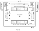
- FIGS. 3A , 3 B, 3 C, 3 D and 3 E are block diagrams of CAM systems in accordance with alternate embodiments of the present invention.
- FIG. 1 is a block diagram of a CAM system 150 in accordance with one embodiment of the present invention.
- CAM system 150 includes a CAM device 100 , an external V DD voltage supply 110 and an external V CORE voltage supply 120 .
- CAM device 100 can be, for example, a packaged integrated circuit die (chip), which is fabricated using conventional semiconductor processing techniques.
- CAM device 100 includes word line control circuit 101 , bit line control circuit 102 , search line control circuit 103 , match line control circuit 104 , CAM array 105 , V DD supply pad 111 , V CORE supply pad 121 and logic & control circuitry 130 .
- logic & control circuitry 130 includes conventional circuitry that may support or supplement CAM array 105 and the associated control circuits 101 - 104 .
- CAM array 105 includes M rows and N columns of CAM cells. Each CAM cell in CAM array 105 is labeled 10 R,C , wherein R is the row number of the cell, and C is the column number of the cell. Thus, array 105 includes CAM cells 10 1,1 - 10 M,N . These CAM cells can be, for example, binary or ternary CAM cells. Although CAM cells 10 1,1 - 10 M,N are illustrated as having a NOR-type configuration, it is understood that these CAM cells can have a NAND-type configuration in other embodiments.
- Each row of CAM cells is coupled to a corresponding word line. More specifically, rows 1 through M of CAM array 105 are coupled to word lines W 1 -W M , respectively. Word lines W 1 -W M are coupled to word line control circuit 101 .
- Each row of CAM cells is also coupled to a corresponding match line. More specifically, rows 1 through M of CAM array 105 are coupled to match lines M 1 -M M , respectively. Match lines M 1 -M M are coupled to match line control circuit 104 .
- Each column of CAM cells is coupled to a corresponding complementary bit line pair. More specifically, columns 1 through N of CAM array 105 are coupled to bit line pairs B 1 -B 1# to B N -B N# , respectively.
- Bit line pairs B 1 -B 1# to B N -B N# are coupled to bit line control circuit 102 .
- Each column of CAM cells is also coupled to a corresponding complementary search line pair. More specifically, columns 1 through N of CAM array 105 are coupled to search line pairs S 1 -S 1# to S N -S N# , respectively. Search line pairs S 1 -S 1# to S N -S N# , are coupled to search line control circuit 103 .
- Word line control circuit 101 , bit line control circuit 102 and logic & control circuitry 130 are coupled to V DD supply pad 111 .
- V DD supply pad 111 is coupled to receive a V DD supply voltage from external V DD voltage supply 110 .
- word line control circuit 101 , bit line control circuit 102 and logic & control circuitry 130 operate in response to the V DD supply voltage.
- Search line control circuit 103 and match line control circuit 104 are coupled to V CORE supply pad 121 .
- V CORE supply pad 121 is coupled to receive a V CORE supply voltage from external V CORE voltage supply 120 .
- search line control circuit 103 and match line control circuit 104 operate in response to the V CORE supply voltage.
- the V CORE supply voltage is less than the V DD supply voltage. Selection of the V CORE supply voltage is described in more detail below.
- V CORE supply pad 121 can be made, for example, through a printed circuit board, wherein the V CORE supply pad 121 is connected to the printed circuit board by a pin or a solder ball in a manner well known by those of ordinary skill in the art.
- V CORE supply pad 121 and one V DD supply pad 111 is illustrated in FIG. 1 , it is understood that CAM device 100 may include multiple V CORE supply pads and/or multiple V DD supply pads in alternate embodiments of the present invention.
- Word line control circuit 101 and bit line control circuit 102 implement read and write operations to CAM array 105 in a well-known manner, which is briefly described below.
- Word line control circuit 101 and bit line control circuit 102 may be collectively referred to as read/write access circuitry.
- bit line control circuit 102 applies the data to be written on bit line pairs B 1 -B 1# to B N -B N# .
- Word line control circuit 101 activates a word line signal on the word line of the row to be written. Under these conditions, the data provided on the bit lines is written to the CAM cells of the selected row.
- word line control circuit 101 and bit line control circuit 102 operate in response to the V DD supply voltage.
- the complementary bit lines have a signal swing from ground (0 Volts) to the V DD supply voltage.
- bit line control circuit 102 may provide a logic ‘1’ data value on complementary bit line pair B 1 -B 1# by applying the V DD supply voltage to bit line B 1 , and coupling complementary bit line B 1# to ground.
- the word lines also have a signal swing from ground to the V DD supply voltage.
- word line control circuit 101 may activate the word line W 1 by applying the V DD supply voltage to this word line, and de-activate the word line W 1 by coupling this word line to ground.
- word line control circuit 101 activates a word line of the row to be read
- bit line control circuit 102 activates internal sense amplifiers (not shown), which are coupled to complementary bit line pairs B 1 -B 1# to B N -B N# .
- the data stored in the CAM cells of the selected row is applied to the complementary bit line pairs.
- the enabled sense amplifiers within bit line control circuit 102 amplify the data signals on the bit line pairs, such that these data signals have a full signal swing equal to the V DD supply voltage. For example, a sense amplifier that detects a logic ‘1’ data value on complementary bit line pair B 1 -B 1# will pull bit line B 1 up to the V DD supply voltage, and pull complementary bit line B 1# down to ground.
- Word line control circuit 101 and bit line control circuit 102 implement read and write operations to CAM array 105 in a well-known manner, which is briefly described below.
- Word line control circuit 101 and bit line control circuit 102 may be collectively referred to as read/write access circuitry.
- search line control circuit 103 and match line control circuit 104 may implement search operations to CAM array 105 in the manner described below.
- Search line control circuit 103 and match line control circuit 104 may be collectively referred to as comparison access circuitry.
- both search line control circuit 103 and match line control circuit 104 operate in response to the V CORE supply voltage.
- Match line control circuit 104 initially pre-charges match lines M 1 -M M to the V CORE supply voltage.
- Search line control circuit 103 then applies search data to the complementary search line pairs S 1 -S 1# to S N -S N# .
- the search data signals have a full signal swing equal to the V CORE supply voltage.
- search line control circuit 103 may apply a logic ‘1’ search data value on complementary search line pair S 1 -S 1# by applying the V CORE supply voltage to search line S 1 , and coupling the complementary search line S 1# to ground.
- the search data values are compared with the data values stored in CAM cells. If the search data value applied to a CAM cell does not match the data value stored in the CAM cell, then the CAM cell discharges the associated match line to ground, thereby indicating a non-match condition. However, if the search data value applied to a CAM cell matches the data value stored in the CAM cell, then the CAM cell does not discharge the associated match line to ground. If each CAM cell in a given row stores a data value that matches the applied search data value, then the match line associated with this row is not discharged, and remains charged at (or near) the V CORE supply voltage to identify a matching condition. Note that the maximum signal swing on the match lines M 1 -M M is advantageously limited to the V CORE supply voltage.
- Match line control circuit 104 includes comparator circuitry that monitors the match lines to determine which (if any) of the match lines remain charged at the end of the search operation, thereby identifying any rows that store data that matches the applied search data.
- Match line control circuit 104 may also include a priority encoder that identifies the matching row having the highest assigned priority. As is well known in the art, the address of this highest priority matching row can be used to access another memory (not shown).
- search line control circuit 103 and match line control circuit 104 do not require special circuitry to drive and receive low swing signals.
- Reducing the signal swing on the search lines S 1 -S 1# to S N -S N# and the match lines M 1 -M M advantageously reduces the power consumed during search operations.
- CAM device 100 operates in response to a V DD supply voltage of 1.0 Volts and a V CORE supply voltage of 0.7 Volts.
- the power consumption of CAM device 100 is reduced by about 49% (i.e., 0.7*0.7) with respect to a conventional CAM device that operates the search line control circuit 103 and the match line control circuit 104 in response to the V DD supply voltage of 1.0 Volts.
- the search line control circuit 103 and the match line control circuit 104 can be over-designed.
- the transistors that operate in response to the V CORE supply voltage must be made larger than the transistors that operate in response to the V DD supply voltage. That is, the widths of timing-critical transistors that operate in response to the V CORE supply voltage are made larger to allow these transistors to meet the same speed performance as the transistors that operate in response to the V DD supply voltage. Because the search line and match line capacitances are dominated by wire and CAM cell capacitances, over-designing the search line control circuit 103 and the match line control circuit 104 will not add significant capacitance to the CAM device 100 .
- the circuitry selected to operate in response to the V CORE supply voltage is preferably limited to the most power consuming circuitry of the chip.
- FIG. 2 is a flow diagram 200 illustrating the manner in which the nominal value of the V CORE supply voltage is selected in accordance with one embodiment of the present invention.
- this CAM device is coupled to the external V DD voltage supply 110 , such that the word line control circuit 101 and the bit line control circuit 102 receive the V DD supply voltage (Step 201 ).
- the CAM device 100 is also coupled to an adjustable external V CORE voltage supply 120 , such that the search line control circuit 103 and the match line control circuit 104 receive the V CORE supply voltage (Step 202 ).
- the V CORE supply voltage is selected to have an initial value, which is less than or equal to the V DD supply voltage (Step 202 ).
- the initial value of the V CORE supply voltage is selected to have a value greater than the expected final V CORE supply voltage.
- the operating characteristics of the CAM device 100 are then tested at the selected V DD and V CORE voltages (Step 203 ). More specifically, test data is written to the CAM array 105 , and search operations are then performed to determine whether matching and non-matching conditions are reliably detected at the selected operating speed. If testing indicates that search operations can be reliably performed at the selected operating speed (Step 204 , Yes branch), then the V CORE voltage supply 120 is adjusted to reduce the V CORE supply voltage (Step 205 ). Processing then returns to Step 203 , wherein the operating characteristics of the CAM device 100 are tested at the reduced V CORE supply voltage.
- Step 204 a final value of the V CORE supply voltage is selected from the V CORE supply voltages that provided reliable performance at the selected operating speed (Step 206 ).
- the V CORE voltage supply 120 used to supply the CAM device 100 during normal operation of CAM system 150 is configured to provide this final value of the V CORE supply voltage.
- CAM system 150 is controlled to operate reliably at a desired speed, with minimum power consumption.
- Step 203 can be modified such that the CAM device is tested to determine the fastest reliable operating speed for the selected V CORE supply voltage. The final value of the V CORE supply voltage would then be selected to be the lowest V CORE supply voltage that provided reliable operation at the desired operating speed of CAM device 150 .
- FIGS. 3A , 3 B, 3 C, 3 D and 3 E are block diagrams that illustrate the manner in which the V CORE supply voltage may be applied to the control circuits 101 - 104 in accordance with alternate embodiments of the present invention. Similar elements are labeled with similar reference numbers in FIGS. 1 and 3 A- 3 E. Note that the logic & control circuitry 103 is coupled to receive the V DD supply voltage in each of the alternate embodiments represented by FIGS. 3A-3E . Also note that at least one of the search line control circuit 103 and the match line control circuit 104 is supplied with the V CORE supply voltage in each of these alternate embodiments.
- the V CORE supply voltage may be used to operate search line control circuit 103 , while the word line control circuit 101 , bit line control circuit 102 and match line control circuit 104 operate in response to the V DD supply voltage.
- power savings are realized due to the reduced swing of the search line signal S 1 -S 1# to S N -S N# .
- Match line signals M 1 -M M undergo a full signal swing equal to the V DD supply voltage, which may result in more reliable determination of match/non-match conditions.
- the V CORE supply voltage may be used to operate match line control circuit 104 , while the word line control circuit 101 , bit line control circuit 102 and search line control circuit 103 operate in response to the V DD supply voltage.
- power savings are realized due to the reduced swing of the match line signals M 1 -M M .
- Search line signals S 1 -S 1# to S N -S N# undergo a full signal swing equal to the V DD supply voltage, which may result in faster determination of match/non-match conditions.
- the V CORE supply voltage may be used to operate bit line control circuit 102 , search line control circuit 103 and match line control circuit 104 , while the word line control circuit 101 operates in response to the V DD supply voltage.
- power savings are realized due to the reduced swing of the bit line signals B 1 -B 1# to B N -B N# , the search line signals S 1 -S 1# to S N -S N# , and the match line signals M 1 -M M .
- Word line signals W 1 -W M undergo a full signal swing equal to the V DD supply voltage, which may result in faster and more reliable read and write operations.
- the V CORE supply voltage may be used to operate word line control circuit 101 , search line control circuit 103 and match line control circuit 104 , while the bit line control circuit 102 operates in response to the V DD supply voltage.
- power savings are realized due to the reduced swing of the word line signals W 1 -W M , the search line signals S 1 -S 1# to S N -S N# , and the match line signals M 1 -M M .
- Bit line signals B 1 -B 1# to B N -B N# undergo a full signal swing equal to the V DD supply voltage, which may result in faster and more reliable read and write operations.
- the V CORE supply voltage may be used to operate word line control circuit 101 , bit line control circuit 102 , search line control circuit 103 and match line control circuit 104 .
- power savings are realized due to the reduced swing of the word line signals W 1 -W M , the bit line signals B 1 -B 1# to B N -B N# , the search line signals S 1 -S 1# to S N -S N# , and the match line signals M 1 -M M .
Landscapes
- Engineering & Computer Science (AREA)
- Power Engineering (AREA)
- Dram (AREA)
Abstract
Description
Claims (19)
Priority Applications (1)
| Application Number | Priority Date | Filing Date | Title |
|---|---|---|---|
| US12/197,549 US7692941B2 (en) | 2008-08-25 | 2008-08-25 | Separate CAM core power supply for power saving |
Applications Claiming Priority (1)
| Application Number | Priority Date | Filing Date | Title |
|---|---|---|---|
| US12/197,549 US7692941B2 (en) | 2008-08-25 | 2008-08-25 | Separate CAM core power supply for power saving |
Publications (2)
| Publication Number | Publication Date |
|---|---|
| US20100046265A1 US20100046265A1 (en) | 2010-02-25 |
| US7692941B2 true US7692941B2 (en) | 2010-04-06 |
Family
ID=41696237
Family Applications (1)
| Application Number | Title | Priority Date | Filing Date |
|---|---|---|---|
| US12/197,549 Expired - Fee Related US7692941B2 (en) | 2008-08-25 | 2008-08-25 | Separate CAM core power supply for power saving |
Country Status (1)
| Country | Link |
|---|---|
| US (1) | US7692941B2 (en) |
Cited By (3)
| Publication number | Priority date | Publication date | Assignee | Title |
|---|---|---|---|---|
| US20110169562A1 (en) * | 2010-01-08 | 2011-07-14 | Mindspeed Technologies, Inc. | System on chip power management through package configuration |
| US8274265B1 (en) | 2007-02-28 | 2012-09-25 | Netlogic Microsystems, Inc. | Multi-phase power system with redundancy |
| TWI806334B (en) * | 2021-01-08 | 2023-06-21 | 新加坡商聯發科技(新加坡)私人有限公司 | A content addressable memory and the operating method thereof |
Families Citing this family (3)
| Publication number | Priority date | Publication date | Assignee | Title |
|---|---|---|---|---|
| US8719475B2 (en) * | 2010-07-13 | 2014-05-06 | Broadcom Corporation | Method and system for utilizing low power superspeed inter-chip (LP-SSIC) communications |
| KR20190041071A (en) * | 2017-10-12 | 2019-04-22 | 에스케이하이닉스 주식회사 | Memory chip, package device and operating method thereof |
| CN110797066B (en) * | 2019-10-31 | 2020-08-04 | 新华三半导体技术有限公司 | Voltage swing amplitude control circuit of CAM (computer-aided manufacturing) match line |
Citations (1)
| Publication number | Priority date | Publication date | Assignee | Title |
|---|---|---|---|---|
| US7471537B1 (en) * | 2006-06-23 | 2008-12-30 | Integrated Device Technology, Ltd. | Content addressable memories (CAM) having low power dynamic match line sensing circuits therein |
-
2008
- 2008-08-25 US US12/197,549 patent/US7692941B2/en not_active Expired - Fee Related
Patent Citations (1)
| Publication number | Priority date | Publication date | Assignee | Title |
|---|---|---|---|---|
| US7471537B1 (en) * | 2006-06-23 | 2008-12-30 | Integrated Device Technology, Ltd. | Content addressable memories (CAM) having low power dynamic match line sensing circuits therein |
Cited By (6)
| Publication number | Priority date | Publication date | Assignee | Title |
|---|---|---|---|---|
| US8274265B1 (en) | 2007-02-28 | 2012-09-25 | Netlogic Microsystems, Inc. | Multi-phase power system with redundancy |
| US8836306B2 (en) | 2007-02-28 | 2014-09-16 | Netlogic Microsystems, Inc. | Multi-phase power system with redundancy |
| US8901909B2 (en) | 2007-02-28 | 2014-12-02 | Netlogic Microsystems, Inc. | Multi-phase power system with redundancy |
| US20110169562A1 (en) * | 2010-01-08 | 2011-07-14 | Mindspeed Technologies, Inc. | System on chip power management through package configuration |
| US8717093B2 (en) * | 2010-01-08 | 2014-05-06 | Mindspeed Technologies, Inc. | System on chip power management through package configuration |
| TWI806334B (en) * | 2021-01-08 | 2023-06-21 | 新加坡商聯發科技(新加坡)私人有限公司 | A content addressable memory and the operating method thereof |
Also Published As
| Publication number | Publication date |
|---|---|
| US20100046265A1 (en) | 2010-02-25 |
Similar Documents
| Publication | Publication Date | Title |
|---|---|---|
| US6418067B1 (en) | Semiconductor memory device suitable for merging with logic | |
| US9424891B2 (en) | Methods and devices for temperature sensing of a memory device | |
| US7692941B2 (en) | Separate CAM core power supply for power saving | |
| US7593272B2 (en) | Detection of row-to-row shorts and other row decode defects in memory devices | |
| JP3673027B2 (en) | Semiconductor memory device having semiconductor memory circuit to be tested | |
| US8072820B2 (en) | System and method for reducing pin-count of memory devices, and memory device testers for same | |
| JP2000036200A (en) | Integrated circuit chip, its operating method and dram | |
| KR102104188B1 (en) | Apparatus and methods for terminating low power states in memory devices | |
| KR20150033101A (en) | Semiconductor device and system including the same | |
| JP5030336B2 (en) | Semiconductor integrated circuit device | |
| TW200933642A (en) | Method and apparatus for increasing yield in an electronic circuit | |
| JP2003168299A (en) | Memory circuit having compression test function | |
| TW559820B (en) | Method to test several word-lines of a semiconductor-memory arrangement | |
| US20060221690A1 (en) | Test mode for detecting a floating word line | |
| US20080237587A1 (en) | Method and circuit for stressing upper level interconnects in semiconductor devices | |
| US6333882B1 (en) | Equilibration/pre-charge circuit for a memory device | |
| US6590819B1 (en) | Digit line equilibration using time-multiplexed isolation | |
| US7760564B2 (en) | Non-volatile memory structure | |
| US7620835B2 (en) | Voltage supply control device and method | |
| KR100626385B1 (en) | Semiconductor memory device and multi-chip package having the same | |
| EP0809178B1 (en) | Multiple-bit comparator with reliable output timing and reduced hazards | |
| US7120070B2 (en) | Method for testing the serviceability of bit lines in a DRAM memory device | |
| US7046562B2 (en) | Integrated circuit reset circuitry | |
| JP2002190527A (en) | Semiconductor integrated circuit | |
| US6469946B2 (en) | Semiconductor memory and its test method |
Legal Events
| Date | Code | Title | Description |
|---|---|---|---|
| AS | Assignment |
Owner name: INTEGRATED DEVICE TECHNOLOGY, INC.,CALIFORNIA Free format text: ASSIGNMENT OF ASSIGNORS INTEREST;ASSIGNORS:CHU, SCOTT;PARK, KEE;REEL/FRAME:021436/0397 Effective date: 20080822 |
|
| AS | Assignment |
Owner name: SILICON VALLEY BANK,CALIFORNIA Free format text: SECURITY AGREEMENT;ASSIGNORS:NETLOGIC MICROSYSTEMS, INC.;NETLOGIC MICROSYSTEMS INTERNATIONAL LIMITED;NETLOGIC MICROSYSTEMS CAYMANS LIMITED;REEL/FRAME:022973/0710 Effective date: 20090717 Owner name: SILICON VALLEY BANK, CALIFORNIA Free format text: SECURITY AGREEMENT;ASSIGNORS:NETLOGIC MICROSYSTEMS, INC.;NETLOGIC MICROSYSTEMS INTERNATIONAL LIMITED;NETLOGIC MICROSYSTEMS CAYMANS LIMITED;REEL/FRAME:022973/0710 Effective date: 20090717 |
|
| AS | Assignment |
Owner name: NETLOGIC MICROSYSTEMS, INC.,CALIFORNIA Free format text: ASSIGNMENT OF ASSIGNORS INTEREST;ASSIGNOR:INTEGRATED DEVICE TECHNOLOGY, INC.;REEL/FRAME:022997/0607 Effective date: 20090717 |
|
| FEPP | Fee payment procedure |
Free format text: PAYOR NUMBER ASSIGNED (ORIGINAL EVENT CODE: ASPN); ENTITY STATUS OF PATENT OWNER: LARGE ENTITY Free format text: PAYER NUMBER DE-ASSIGNED (ORIGINAL EVENT CODE: RMPN); ENTITY STATUS OF PATENT OWNER: LARGE ENTITY |
|
| STCF | Information on status: patent grant |
Free format text: PATENTED CASE |
|
| AS | Assignment |
Owner name: NETLOGIC MICROSYSTEMS CAYMANS LIMITED, CALIFORNIA Free format text: RELEASE BY SECURED PARTY;ASSIGNOR:SILICON VALLEY BANK;REEL/FRAME:026830/0141 Effective date: 20110826 Owner name: NETLOGIC MICROSYSTEMS INTERNATIONAL LIMITED, CALIF Free format text: RELEASE BY SECURED PARTY;ASSIGNOR:SILICON VALLEY BANK;REEL/FRAME:026830/0141 Effective date: 20110826 Owner name: NETLOGIC MICROSYSTEMS, INC., CALIFORNIA Free format text: RELEASE BY SECURED PARTY;ASSIGNOR:SILICON VALLEY BANK;REEL/FRAME:026830/0141 Effective date: 20110826 |
|
| FPAY | Fee payment |
Year of fee payment: 4 |
|
| AS | Assignment |
Owner name: NETLOGIC I LLC, DELAWARE Free format text: CHANGE OF NAME;ASSIGNOR:NETLOGIC MICROSYSTEMS, INC.;REEL/FRAME:035443/0824 Effective date: 20130123 Owner name: BROADCOM CORPORATION, CALIFORNIA Free format text: ASSIGNMENT OF ASSIGNORS INTEREST;ASSIGNOR:NETLOGIC I LLC;REEL/FRAME:035443/0763 Effective date: 20150327 |
|
| AS | Assignment |
Owner name: BANK OF AMERICA, N.A., AS COLLATERAL AGENT, NORTH CAROLINA Free format text: PATENT SECURITY AGREEMENT;ASSIGNOR:BROADCOM CORPORATION;REEL/FRAME:037806/0001 Effective date: 20160201 Owner name: BANK OF AMERICA, N.A., AS COLLATERAL AGENT, NORTH Free format text: PATENT SECURITY AGREEMENT;ASSIGNOR:BROADCOM CORPORATION;REEL/FRAME:037806/0001 Effective date: 20160201 |
|
| AS | Assignment |
Owner name: AVAGO TECHNOLOGIES GENERAL IP (SINGAPORE) PTE. LTD., SINGAPORE Free format text: ASSIGNMENT OF ASSIGNORS INTEREST;ASSIGNOR:BROADCOM CORPORATION;REEL/FRAME:041706/0001 Effective date: 20170120 Owner name: AVAGO TECHNOLOGIES GENERAL IP (SINGAPORE) PTE. LTD Free format text: ASSIGNMENT OF ASSIGNORS INTEREST;ASSIGNOR:BROADCOM CORPORATION;REEL/FRAME:041706/0001 Effective date: 20170120 |
|
| AS | Assignment |
Owner name: BROADCOM CORPORATION, CALIFORNIA Free format text: TERMINATION AND RELEASE OF SECURITY INTEREST IN PATENTS;ASSIGNOR:BANK OF AMERICA, N.A., AS COLLATERAL AGENT;REEL/FRAME:041712/0001 Effective date: 20170119 |
|
| MAFP | Maintenance fee payment |
Free format text: PAYMENT OF MAINTENANCE FEE, 8TH YEAR, LARGE ENTITY (ORIGINAL EVENT CODE: M1552) Year of fee payment: 8 |
|
| AS | Assignment |
Owner name: AVAGO TECHNOLOGIES INTERNATIONAL SALES PTE. LIMITE Free format text: MERGER;ASSIGNOR:AVAGO TECHNOLOGIES GENERAL IP (SINGAPORE) PTE. LTD.;REEL/FRAME:047196/0687 Effective date: 20180509 |
|
| AS | Assignment |
Owner name: AVAGO TECHNOLOGIES INTERNATIONAL SALES PTE. LIMITE Free format text: CORRECTIVE ASSIGNMENT TO CORRECT THE EFFECTIVE DATE OF MERGER TO 9/5/2018 PREVIOUSLY RECORDED AT REEL: 047196 FRAME: 0687. ASSIGNOR(S) HEREBY CONFIRMS THE MERGER;ASSIGNOR:AVAGO TECHNOLOGIES GENERAL IP (SINGAPORE) PTE. LTD.;REEL/FRAME:047630/0344 Effective date: 20180905 |
|
| AS | Assignment |
Owner name: AVAGO TECHNOLOGIES INTERNATIONAL SALES PTE. LIMITE Free format text: CORRECTIVE ASSIGNMENT TO CORRECT THE PROPERTY NUMBERS PREVIOUSLY RECORDED AT REEL: 47630 FRAME: 344. ASSIGNOR(S) HEREBY CONFIRMS THE ASSIGNMENT;ASSIGNOR:AVAGO TECHNOLOGIES GENERAL IP (SINGAPORE) PTE. LTD.;REEL/FRAME:048883/0267 Effective date: 20180905 |
|
| FEPP | Fee payment procedure |
Free format text: MAINTENANCE FEE REMINDER MAILED (ORIGINAL EVENT CODE: REM.); ENTITY STATUS OF PATENT OWNER: LARGE ENTITY |
|
| LAPS | Lapse for failure to pay maintenance fees |
Free format text: PATENT EXPIRED FOR FAILURE TO PAY MAINTENANCE FEES (ORIGINAL EVENT CODE: EXP.); ENTITY STATUS OF PATENT OWNER: LARGE ENTITY |
|
| STCH | Information on status: patent discontinuation |
Free format text: PATENT EXPIRED DUE TO NONPAYMENT OF MAINTENANCE FEES UNDER 37 CFR 1.362 |
|
| FP | Lapsed due to failure to pay maintenance fee |
Effective date: 20220406 |