US7687333B2 - Method of fabricating thin film transistor and array substrate for liquid crystal display device including the same - Google Patents
Method of fabricating thin film transistor and array substrate for liquid crystal display device including the same Download PDFInfo
- Publication number
- US7687333B2 US7687333B2 US11/965,423 US96542307A US7687333B2 US 7687333 B2 US7687333 B2 US 7687333B2 US 96542307 A US96542307 A US 96542307A US 7687333 B2 US7687333 B2 US 7687333B2
- Authority
- US
- United States
- Prior art keywords
- forming
- layer
- source
- metal layer
- drain electrodes
- Prior art date
- Legal status (The legal status is an assumption and is not a legal conclusion. Google has not performed a legal analysis and makes no representation as to the accuracy of the status listed.)
- Active
Links
Images


Classifications
-
- H—ELECTRICITY
- H10—SEMICONDUCTOR DEVICES; ELECTRIC SOLID-STATE DEVICES NOT OTHERWISE PROVIDED FOR
- H10D—INORGANIC ELECTRIC SEMICONDUCTOR DEVICES
- H10D30/00—Field-effect transistors [FET]
- H10D30/60—Insulated-gate field-effect transistors [IGFET]
- H10D30/67—Thin-film transistors [TFT]
- H10D30/6729—Thin-film transistors [TFT] characterised by the electrodes
- H10D30/6737—Thin-film transistors [TFT] characterised by the electrodes characterised by the electrode materials
-
- H—ELECTRICITY
- H10—SEMICONDUCTOR DEVICES; ELECTRIC SOLID-STATE DEVICES NOT OTHERWISE PROVIDED FOR
- H10D—INORGANIC ELECTRIC SEMICONDUCTOR DEVICES
- H10D30/00—Field-effect transistors [FET]
- H10D30/60—Insulated-gate field-effect transistors [IGFET]
- H10D30/67—Thin-film transistors [TFT]
- H10D30/674—Thin-film transistors [TFT] characterised by the active materials
- H10D30/6741—Group IV materials, e.g. germanium or silicon carbide
- H10D30/6743—Silicon
-
- H—ELECTRICITY
- H10—SEMICONDUCTOR DEVICES; ELECTRIC SOLID-STATE DEVICES NOT OTHERWISE PROVIDED FOR
- H10D—INORGANIC ELECTRIC SEMICONDUCTOR DEVICES
- H10D86/00—Integrated devices formed in or on insulating or conducting substrates, e.g. formed in silicon-on-insulator [SOI] substrates or on stainless steel or glass substrates
- H10D86/01—Manufacture or treatment
- H10D86/021—Manufacture or treatment of multiple TFTs
- H10D86/0231—Manufacture or treatment of multiple TFTs using masks, e.g. half-tone masks
-
- H—ELECTRICITY
- H10—SEMICONDUCTOR DEVICES; ELECTRIC SOLID-STATE DEVICES NOT OTHERWISE PROVIDED FOR
- H10D—INORGANIC ELECTRIC SEMICONDUCTOR DEVICES
- H10D86/00—Integrated devices formed in or on insulating or conducting substrates, e.g. formed in silicon-on-insulator [SOI] substrates or on stainless steel or glass substrates
- H10D86/40—Integrated devices formed in or on insulating or conducting substrates, e.g. formed in silicon-on-insulator [SOI] substrates or on stainless steel or glass substrates characterised by multiple TFTs
- H10D86/441—Interconnections, e.g. scanning lines
-
- H—ELECTRICITY
- H10—SEMICONDUCTOR DEVICES; ELECTRIC SOLID-STATE DEVICES NOT OTHERWISE PROVIDED FOR
- H10D—INORGANIC ELECTRIC SEMICONDUCTOR DEVICES
- H10D86/00—Integrated devices formed in or on insulating or conducting substrates, e.g. formed in silicon-on-insulator [SOI] substrates or on stainless steel or glass substrates
- H10D86/40—Integrated devices formed in or on insulating or conducting substrates, e.g. formed in silicon-on-insulator [SOI] substrates or on stainless steel or glass substrates characterised by multiple TFTs
- H10D86/60—Integrated devices formed in or on insulating or conducting substrates, e.g. formed in silicon-on-insulator [SOI] substrates or on stainless steel or glass substrates characterised by multiple TFTs wherein the TFTs are in active matrices
-
- H—ELECTRICITY
- H10—SEMICONDUCTOR DEVICES; ELECTRIC SOLID-STATE DEVICES NOT OTHERWISE PROVIDED FOR
- H10P—GENERIC PROCESSES OR APPARATUS FOR THE MANUFACTURE OR TREATMENT OF DEVICES COVERED BY CLASS H10
- H10P14/00—Formation of materials, e.g. in the shape of layers or pillars
- H10P14/40—Formation of materials, e.g. in the shape of layers or pillars of conductive or resistive materials
- H10P14/42—Formation of materials, e.g. in the shape of layers or pillars of conductive or resistive materials using a gas or vapour
- H10P14/44—Physical vapour deposition [PVD]
-
- H—ELECTRICITY
- H10—SEMICONDUCTOR DEVICES; ELECTRIC SOLID-STATE DEVICES NOT OTHERWISE PROVIDED FOR
- H10W—GENERIC PACKAGES, INTERCONNECTIONS, CONNECTORS OR OTHER CONSTRUCTIONAL DETAILS OF DEVICES COVERED BY CLASS H10
- H10W20/00—Interconnections in chips, wafers or substrates
- H10W20/01—Manufacture or treatment
- H10W20/031—Manufacture or treatment of conductive parts of the interconnections
- H10W20/032—Manufacture or treatment of conductive parts of the interconnections of conductive barrier, adhesion or liner layers
Definitions
- the present invention relates to a liquid crystal display (LCD) device and more particularly to a method of fabricating a thin film transistor (TFT) and an array substrate for an LCD device including the TFT.
- LCD liquid crystal display
- TFT thin film transistor
- Plat panel display devices such as an LCD device, a plasma display panel (PDP), a vacuum fluorescent display (VFD) device and an organic electroluminescent display (OELD) device, have been developed.
- LCD liquid crystal display
- PDP plasma display panel
- VFD vacuum fluorescent display
- OELD organic electroluminescent display
- LCD devices since the LCD device has a smaller size, lower power consumption than a display device using cathode-ray tubes (CRT), the display device using CRT is replaced by the LCD device. Also, LCD devices are widely used for notebook computers, monitors, TV, and so on, because of their high contrast ratio and characteristics adequate to display moving images.
- CTR cathode-ray tubes
- the LCD device uses optical anisotropy and polarization properties of liquid crystal molecules to display images.
- the LCD device includes an array substrate including a thin film transistor (TFT) as a switching element and a pixel electrode, a color filter substrate including a color filter layer and a common electrode, and a liquid crystal layer having the liquid crystal molecules.
- TFT thin film transistor
- the liquid crystal layer is interposed between the array substrate and the color filter substrate so as to be driven by a vertical electric field induced between the pixel and common electrodes.
- FIG. 1 is a schematic plan view of an array substrate for an LCD device according to the related art
- FIG. 2 is a cross-sectional view taken along the line II-II in FIG. 1 .
- a gate line 20 , a gate electrode 25 , an active layer 40 , a source electrode 32 and a drain electrode 34 , a data line 30 , and a pixel electrode 70 are formed on a substrate 10 having a pixel region P.
- the gate and data lines 20 and 30 cross each other to define the pixel region P.
- the gate electrode 25 is connected to the gate line 20
- the active layer 40 is formed over the gate electrode 25 .
- the source electrode 32 is connected to the data line 30 and spaced apart from the drain electrode 34 .
- the gate electrode 25 , the active layer 40 , an ohmic contact layer (not shown), the source electrode 32 and the drain electrode 34 constitute a thin film transistor (TFT) T.
- TFT thin film transistor
- the pixel electrode 50 is formed in the pixel region “P” to be connected to the drain electrode 34 through a drain contact hole H 1 .
- a barrier metal pattern is formed on the ohmic contact layer (not shown) and under the source and drain electrodes 32 and 34 .
- FIG. 2 A method of fabricating an array substrate is explained with FIG. 2 .
- the gate electrode 25 is formed on the substrate 10 by depositing and patterning a first metal layer (not shown).
- the gate line 20 (of FIG. 1 ) is formed from the first metal layer (not shown).
- an inorganic insulating material such as silicon nitride (SiNx) and silicon oxide (SiO2), is deposited on an entire surface of the substrate 10 including the gate electrode 25 and the gate line 20 (of FIG. 1 ) to form a gate insulating layer 45 .
- the active layer 40 and the impurity-doped amorphous silicon layer are sequentially formed on the gate insulating layer 45 .
- the active layer 40 and the impurity-doped amorphous silicon layer (not shown) overlap the gate electrode 25 .
- the active layer 40 and the impurity-doped amorphous silicon layer (not shown) may be formed by a plasma enhanced chemical vapor deposition (PECVD).
- PECVD plasma enhanced chemical vapor deposition
- the active layer 40 is formed of intrinsic amorphous silicon, while the impurity-doped amorphous silicon layer (not shown) is formed of impurity-doped amorphous silicon.
- the ohmic contact layer 41 is formed of intrinsic amorphous silicon, while the impurity-doped amorphous silicon layer (not shown) is formed of impurity-doped amorphous silicon.
- a barrier metal layer (not shown) and a second metal layer (not shown) are sequentially formed on the ohmic contact layer 41 .
- the barrier metal layer (not shown) is formed of one of titanium (Ti), molybdenum (Mo) and molybdenum-titanium (MoTi) alloy, and the second metal layer (not shown) is formed of copper (Cu).
- the second metal layer (not shown) is sequentially patterned to form the source and drain electrodes 32 and 34 .
- the data line 30 (of FIG. 1 ) is formed.
- the barrier metal layer (not shown) and the impurity-doped amorphous silicon layer (not shown) are patterned using the source and drain electrodes 32 and 34 to form a barrier metal pattern 35 and the ohmic contact layer 41 .
- a portion of the active layer 40 is exposed between the ohmic contact layer 41 .
- the exposed portion of the active layer 40 is defined as a channel region.
- the gate electrode 25 , the active layer 40 , the ohmic contact layer 41 , the source electrode 32 and the drain electrode 34 constitute the thin film transistor (TFT) T.
- an inorganic insulating material such as silicon nitride (SiNx) and silicon oxide (SiO2), is deposited to form a passivation layer 55 is foiled on the source and drain electrodes 32 and 34 . And then, the passivation layer 55 is patterned to form the drain contact hole H 1 exposing a portion of the drain electrode 34 .
- a pixel electrode 70 of a transparent conductive material is formed on the passivation layer 55 and in the pixel region P.
- the pixel electrode 70 is connected to the drain electrode 34 through the drain contact hole H 1 .
- the barrier metal pattern 35 is formed of one of Ti, Mo and MoTi alloy to prevent a Cu material in the source and drain electrodes 32 and 34 being diffused. Since the source and drain electrodes 32 and 34 and the barrier metal pattern 35 are formed of different material, two deposition processes are required. Moreover, since different type etchants should be used, fabricating process becomes complicated.
- a deposition layer when a MoTi alloy target is used in a sputtering device, a deposition layer includes a relatively high impurity concentration. Accordingly, the deposition layer has a low adhesive strength to lower or/and upper layers.
- the present invention is directed to a method of a thin film transistor and an array substrate for an LCD device including the same that substantially obviates one or more of the problems due to limitations and disadvantages of the related art.
- a method of fabricating a thin film transistor comprises forming a gate electrode on a substrate; forming a gate insulating layer on the gate electrode; forming a semiconductor layer on the gate insulating layer, the semiconductor layer corresponding to the gate electrode; forming first and second barrier patterns on the semiconductor layer, the first and second barrier patterns including copper nitride; and forming source and drain electrodes on the first and second barrier patterns, respectively, the source and drain electrodes including pure copper.
- a method of fabricating an array substrate for a liquid crystal display device comprises forming a gate electrode and a gate line on a substrate, the gate electrode connected to the gate line; forming a gate insulating layer on the gate electrode and the gate line; forming a semiconductor layer on the gate insulating layer, the semiconductor layer corresponding to the gate electrode; forming first and second barrier patterns on the semiconductor layer, the first and second barrier patterns including copper nitride; forming a data line and source electrode and drain electrodes, the data line crossing the gate line and connected to the source electrode, the source and drain electrodes on the first and second barrier patterns, respectively, and including pure copper; and forming a pixel electrode connected to the drain electrode.
- FIG. 1 is a schematic plan view of an array substrate for an LCD device according to the related art.
- FIG. 2 is a cross-sectional view taken along the line II-II in FIG. 1 .
- FIGS. 3A to 3G are cross-sectional views showing fabricating processes of a portion of an array substrate for an LCD device including a TFT according to the present invention.
- FIGS. 4A to 4G are cross-sectional views showing fabricating processes of a portion of an array substrate for an LCD device including a TFT according to the present invention.
- FIG. 5 is a scanning electron microscope (SEM) picture of a portion of a thin film transistor according to the present invention.
- FIG. 6 is a graph showing a specific resistivity of a thin film transistor depending on a temperature.
- FIGS. 3A to 3G are cross-sectional views showing fabricating processes of a portion of an array substrate for an LCD device including a TFT according to the present invention.
- a pixel region P including a switching region S is defined.
- a first metal layer (not shown) is formed on the substrate 110 and then patterned through a first mask process to form a gate electrode 125 in the switching region S.
- a gate line (not shown), which is connected to the gate electrode 125 , is formed on the substrate 110 .
- an inorganic insulating material such as silicon nitride (SiNx) and silicon oxide (SiO2), is deposited on an entire surface of the substrate 110 including the gate electrode 25 and the gate line 20 (of FIG. 1 ) to form a gate insulating layer 145 .
- an intrinsic amorphous silicon layer (not shown) and an impurity-doped amorphous silicon layer (not shown) are sequentially formed the gate insulating layer 145 .
- the intrinsic amorphous silicon layer (not shown) and the impurity-doped amorphous silicon layer (not shown) may be deposited by a chemical vapor deposition (CVD) method.
- the intrinsic amorphous silicon layer (not shown) and the impurity-doped amorphous silicon layer (not shown) are patterned through a second mask process to form an active layer 140 and an impurity-doped amorphous silicon pattern 142 .
- the active layer 140 and the impurity-doped amorphous silicon pattern 142 correspond to the gate electrode 125 . Namely, they are disposed ill the switching region S.
- FIGS. 3C to 3E show a third mask process.
- a second metal layer 128 and a third metal layer 130 are sequentially formed on the substrate 110 including the active layer 140 and the impurity-doped amorphous silicon pattern 142 .
- the second metal layer 128 includes copper nitride (CuN)
- the third metal layer 130 includes pure copper (Cu).
- the second and third metal layers 128 and 130 arc formed in a same sputtering chamber using a pure Cu target and a nitride gas source. In more detail, when a Cu metallic material begins to be deposited with the pure Cu target, a nitride gas is injected into the sputtering chamber.
- the process temperature of the sputtering chamber is less than about 350 centigrade. Accordingly, the second metal layer 128 of copper nitride (CuN) is deposited on an entire surface of the substrate 110 including the impurity-doped amorphous silicon pattern 142 . After forming the second metal layer 128 with a pre-determined thickness, nitride gas injection is stopped. As a result, the third metal layer 130 of pure Cu is deposited on the second metal layer 128 . Because the second and third metal layers 128 and 130 are continuously deposited, it seems that a lower region, where N 2 is rich, and an upper region, where N 2 is deplete, are continuously laminated.
- CuN copper nitride
- a thickness of the summation of the CuN layer and the pure Cu layer has a range with about 50 angstroms to 500 angstroms, and the pure Cu layer has a thickness greater than the CuN layer.
- a photoresist (PR) layer 150 is formed on the third metal layer 130 .
- a mask M having a transmitting portion A 1 and a blocking portion A 2 are disposed over the PR layer 150 .
- the transmitting portion A 1 has a relatively high transmittance so that light through the transmitting portion can completely change the PR layer 150 chemically.
- the blocking portion A 2 shields light completely. Namely, a transmittance of the transmitting portion A 1 is greater than that of the blocking portion A 2 .
- the blocking portion A 2 corresponds to a portion where the third metal layer 130 should remain.
- the blocking portion A 2 corresponds to both end portions of the gate electrode 125 , and the transmitting portion A 1 is disposed between the blocking portions A 2 . Namely, the transmitting portion A 1 corresponds to a central portion of the gate electrode 125 .
- the PR layer 150 is exposed through the mask M and developed to form a PR pattern 151 , as shown in FIG. 3D .
- the PR pattern 151 corresponding to the blocking portion A 2 are formed on the third metal layer 130 to correspond to the both end portion of the gate electrode 125 , and the PR layer 150 corresponding to the transmitting portion A 1 is perfectly removed such that the third metal layer 130 is exposed by the PR pattern 151 . Namely, the third metal layer 130 corresponding to the center portion of the gate electrode 125 is exposed.
- the exposed third metal layer 130 (of FIG. 3D ) and the second metal layer 128 (of FIG. 3D ) are wet-etched using the PR pattern 151 as an etching mask to form source and drain electrodes 132 and 134 from the third metal layer 130 (of FIG. 3D ) and a barrier pattern 135 including firsts and second sub-barrier patterns 135 a and 135 b from the second metal layer 128 , respectively.
- a data line (not shown), which cross the gate line (not shown) to define the pixel region P and is connected to the source electrode 132 , is formed from the third metal layer 130 (of FIG. 3D ).
- the barrier pattern 135 prevents a Cu material in the source and drain electrodes 132 and 134 being diffused into the impurity-doped amorphous silicon pattern 142 from which an ohmic contact layer is formed. Since the second metal layer 128 (of FIG. 3D ) and the third metal layer 130 (of FIG. 3D ) are etched, the impurity-doped amorphous silicon layer 141 (of FIG. 130 ) is exposed.
- the second and third metal layer 128 and 130 include a similar or the same kind metal material, the same etchant, for example, phosphoric acid (H 3 PO 4 ), nitric acid (HNO 3 ), acetic acid (CH 3 COOH) and their mixture with water (H 2 O), may be used for etching them. Accordingly, the fabricating process becomes further simply, and the galvanic corrosion problem in the related art is prevented.
- the same etchant for example, phosphoric acid (H 3 PO 4 ), nitric acid (HNO 3 ), acetic acid (CH 3 COOH) and their mixture with water (H 2 O)
- the second metal layer 128 (of FIG. 3D ) of CuN has an etching rate to the above etchant lower than the third metal layer 130 (of FIG. 3D ) of pure Cu. Accordingly, after being etched, side portions of the barrier pattern 135 have a taper slope having a taper angle with a range of about 30 degrees to about 60 degrees. Referring to FIG. 5 , the taper angle is defined an angle ⁇ between a top surface of an ohmic contact layer 141 and a side surface of the barrier pattern 135 . Accordingly, the barrier pattern 135 has a high adhesive strength to the ohmic contact layer 141 .
- an exposed portion of the impurity-doped amorphous silicon 142 is dry-etched to form an ohmic contact layer 141 including first and second ohmic contact patterns 141 a and 141 b and expose a portion of the active layer 140 .
- the exposed portion of the active layer 140 is exposed through respective pairs of the first and second ohmic contact patterns 141 a and 141 b , the first and second barrier patterns 135 a and 135 b , and the source and drain electrodes 132 and 134 .
- the active layer 140 and the ohmic contact layer 141 constitute a semiconductor layer.
- the PR pattern 151 (of FIG. 3E ) is removed, and then an inorganic insulating material, such as silicon nitride (SiNx) and silicon oxide (SiO2), is deposited on an entire surface of the substrate 110 including the source and drain electrodes 132 and 134 to form a passivation layer 155 . And then, the passivation layer 155 is patterned through a fourth mask process to form a drain contact hole H 2 exposing a portion of the drain electrode 134 .
- an inorganic insulating material such as silicon nitride (SiNx) and silicon oxide (SiO2)
- a transparent conductive material such as indium-tin-oxide (ITO) and indium-zinc-oxide (IZO) is deposited on the passivation layer 155 and patterned through a fifth mask process to form a pixel electrode 170 .
- the pixel electrode 170 is connected to the drain electrode 134 through the drain contact hole H 2 .
- An array substrate for an LCD device is fabricated by the above-mentioned five mask processes.
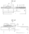
- FIGS. 4A to 4G are cross-sectional views showing fabricating processes of a portion of an array substrate for an LCD device including a TFT according to the present invention.
- FIG. 4A show a first mask process.
- a first metal layer (not shown) is formed on the substrate 210 and then patterned through a first mask process to form a gate electrode 225 in the switching region S.
- a gate line (not shown), which is connected to the gate electrode 225 , is formed on the substrate 210 .
- FIGS. 4B to 4E show a second mask process. Different from a fabricating method explained with FIGS. 3A to 3G , the source and drain electrodes, the barrier pattern, the ohmic contact layer and the active layer are formed through a single mask process in this embodiment.
- a gate insulating layer 245 an intrinsic amorphous silicon layer 238 , an impurity-doped amorphous silicon layer 239 , a second metal layer 226 , a third metal layer 230 , and a PR layer 250 are sequentially formed on an entire surface of the substrate 210 including the gate electrode 225 .
- the gate insulating layer 245 includes an inorganic insulating material, such as silicon nitride (SiNx) and silicon oxide (SiO2).
- the second metal layer 226 includes copper nitride (CuN), while the third metal layer 130 includes pure copper (Cu).
- a thickness of the summation of the CuN layer and the pure Cu layer has a range with about 50 angstroms to 500 angstroms, and the pure Cu layer has a thickness greater than the CuN layer.
- the second and third metal layers 128 and 130 are formed in a same sputtering chamber using a pure Cu target and a nitride gas source. A detailed depositing method is explained with FIG. 3C .
- a mask M having a transmitting portion B 1 , a blocking portion B 2 and a half-transmitting portion B 3 are disposed over the PR layer 250 .
- the transmitting portion B 1 has a relatively high transmittance so that light through the transmitting portion can completely change the PR layer 214 chemically.
- the blocking portion B 2 shields light completely. Namely, a transmittance of the half-transmitting portion B 3 is smaller than that of the transmitting portion B 1 and is greater than that of the blocking portion B 2 .
- the blocking portion B 2 corresponds to a portion where the third metal layer 230 should remain.
- the blocking portion B 2 corresponds to both end portions of the gate electrode 225 , and the half-transmitting portion B 3 is disposed between the blocking portions B 2 .
- the half-transmitting portion B 3 corresponds to a central portion of the gate electrode 225 .
- the PR layer 250 is exposed through the mask M and developed to form first and second PR patterns 251 a and 251 b , as shown in FIG. 4C .
- the first PR pattern 251 a corresponds to the blocking portion B 2
- the second PR pattern 251 b corresponds to the half-transmitting portion B 3 .
- the first and second PR patterns 251 a and 251 b are disposed on the third metal layer 230 corresponding to the switching region S.
- the second PR pattern 251 b corresponds to the center portion of the gate electrode 225 and has a lower thickness than the first PR pattern 251 a .
- the first PR pattern 251 a is also formed to correspond to a portion where the data line is formed. Moreover, since the PR layer 250 (of FIG. 4B ) corresponding to the transmitting portion B 1 of the mask M is perfectly removed such that the third metal layer 230 is exposed.
- an exposed portion of the third metal layer 230 (of FIG. 4C ), the second metal layer 226 (of FIG. 4C ), the impurity-doped amorphous silicon layer 239 (of FIG. 4C ) and the intrinsic amorphous silicon layer 238 (of FIG. 4C ) are etched to form an active layer 240 from the intrinsic amorphous silicon layer 238 (of FIG. 4C ), an impurity-doped amorphous silicon pattern 242 from the impurity-doped amorphous silicon layer 239 (of FIG. 4C ), a barrier metal layer 228 from the second metal layer 226 (of FIG.
- the second metal layer 226 (of FIG. 4C ) and the third metal layer 230 (of FIG. 4C ) are wet-etched using an etchant, such as phosphoric acid (H 3 PO 4 ), nitric acid (HNO 3 ), acetic acid (CH 3 COOH) and their mixture with water (H 2 O), respectively, and the impurity-doped amorphous silicon layer 239 (of FIG. 4C ) and the intrinsic amorphous silicon layer 238 (of FIG. 4C ) are dry-etched.
- an etchant such as phosphoric acid (H 3 PO 4 ), nitric acid (HNO 3 ), acetic acid (CH 3 COOH) and their mixture with water (H 2 O), respectively, and the impurity-doped amorphous silicon layer 239 (of FIG. 4C ) and the intrinsic amorphous silicon layer 238 (of FIG. 4C ) are dry-etched.
- the first PR pattern 251 a (of FIG.
- a third PR pattern 251 c is formed from the first PR pattern 251 a (of FIG. 4C ), and both end portions of the source-drain metal layer 231 are exposed.
- exposed portions of the source-drain metal layer 231 (of FIG. 4D ), the barrier metal layer 228 (of FIG. 4D ) and the impurity-doped amorphous silicon pattern 242 (of FIG. 4D ) are etched to form source and drain electrodes 232 and 234 from the source-drain metal layer 231 (of FIG. 4D ), a barrier pattern 235 including first and second sub-barrier patterns 235 a and 235 b from the barrier metal layer 228 (of FIG. 4D ), and an ohmic contact layer 241 including first and second ohmic contact patterns 241 a and 241 b from the impurity-doped amorphous silicon pattern 242 (of FIG. 4D ).
- the active layer 240 is exposed between the first and second ohmic contact patterns 241 a and 241 b.
- the second and third metal layer 226 and 230 include a similar or the same kind metal material, the same etchant, for example, phosphoric acid (H 3 PO 4 ), nitric acid (HNO 3 ), acetic acid (CH 3 COOH) and their mixture with water (H 2 O), may be used for etching them. Accordingly, the fabricating process becomes further simply, and the galvanic corrosion problem in the related art is prevented.
- the barrier pattern 235 has a high adhesive strength to the ohmic contact layer 241 . The barrier pattern 235 prevents a Cu material in the source and drain electrodes 232 and 234 being diffused into the ohmic contact layer 241 .
- FIG. 4F show a third mask process.
- an inorganic insulating material such as silicon nitride (SiNx) and silicon oxide (SiO2), is deposited on an entire surface of the substrate 210 including the source and drain electrodes 232 and 234 to form a passivation layer 255 .
- the passivation layer 255 is patterned through a third mask process to form a drain contact hole H 3 exposing a portion of the drain electrode 234 .
- a transparent conductive material such as indium-tin-oxide (ITO) and indium-zinc-oxide (IZO) is deposited on the passivation layer 255 and patterned through a fifth mask process to form a pixel electrode 270 .
- the pixel electrode 270 is connected to the drain electrode 234 through the drain contact hole H 2 .
- an array substrate for an LCD device is fabricated by four mask processes.
- FIG. 5 is a scanning electron microscope (SEM) picture of a portion of a thin film transistor according to the present invention.
- SEM scanning electron microscope
- FIG. 6 is a graph showing a specific resistivity of a thin film transistor depending on a temperature.
- the specific resistivity of triple-layered structure which includes the ohmic contact layer of impurity-doped amorphous silicon, the barrier pattern of copper nitride and the source and drain electrodes of pure copper, is inverse proportion to a temperature.
- the layer at asdep has a greatest specific resistivity. Namely, the higher is the temperature, the lower the resistivity is. It means that an ohmic contact property between the ohmic contact layer and each of the source and drain electrodes is improved due to the barrier pattern.
Landscapes
- Thin Film Transistor (AREA)
Abstract
Description
Claims (14)
Applications Claiming Priority (2)
| Application Number | Priority Date | Filing Date | Title |
|---|---|---|---|
| KR10-2007-0025215 | 2007-03-14 | ||
| KR1020070025215A KR20080084084A (en) | 2007-03-14 | 2007-03-14 | Method of manufacturing thin film transistor and array substrate for liquid crystal display device comprising same |
Publications (2)
| Publication Number | Publication Date |
|---|---|
| US20080227243A1 US20080227243A1 (en) | 2008-09-18 |
| US7687333B2 true US7687333B2 (en) | 2010-03-30 |
Family
ID=39763120
Family Applications (1)
| Application Number | Title | Priority Date | Filing Date |
|---|---|---|---|
| US11/965,423 Active US7687333B2 (en) | 2007-03-14 | 2007-12-27 | Method of fabricating thin film transistor and array substrate for liquid crystal display device including the same |
Country Status (2)
| Country | Link |
|---|---|
| US (1) | US7687333B2 (en) |
| KR (1) | KR20080084084A (en) |
Cited By (3)
| Publication number | Priority date | Publication date | Assignee | Title |
|---|---|---|---|---|
| US8753975B1 (en) | 2013-02-01 | 2014-06-17 | Globalfoundries Inc. | Methods of forming conductive copper-based structures using a copper-based nitride seed layer without a barrier layer and the resulting device |
| US8859419B2 (en) | 2013-02-01 | 2014-10-14 | Globalfoundries Inc. | Methods of forming copper-based nitride liner/passivation layers for conductive copper structures and the resulting device |
| CN104882488A (en) * | 2015-06-15 | 2015-09-02 | 合肥鑫晟光电科技有限公司 | Film transistor, array substrate, manufacturing method for array substrate, and display device |
Families Citing this family (7)
| Publication number | Priority date | Publication date | Assignee | Title |
|---|---|---|---|---|
| KR101253497B1 (en) * | 2008-06-02 | 2013-04-11 | 엘지디스플레이 주식회사 | Method of fabricating array substrate for liquid crystal display device |
| CN102090158A (en) * | 2008-07-22 | 2011-06-08 | 国立大学法人东北大学 | Wiring substrate and manufacturing method thereof |
| TWI405017B (en) * | 2008-12-18 | 2013-08-11 | Lg Display Co Ltd | Array substrate of display device and manufacturing method thereof |
| KR101884796B1 (en) * | 2010-12-07 | 2018-08-03 | 엘지디스플레이 주식회사 | Thin film transistor, Flat display device, and Method for fabricating the same |
| KR101968115B1 (en) * | 2012-04-23 | 2019-08-13 | 엘지디스플레이 주식회사 | Array substrate and method of fabricating the same |
| CN103915452B (en) * | 2014-03-28 | 2016-04-06 | 京东方科技集团股份有限公司 | A kind of array base palte, its manufacture method and display unit |
| KR102826432B1 (en) * | 2020-02-10 | 2025-06-30 | 삼성디스플레이 주식회사 | Display apparatus and manufacturing the same |
Citations (4)
| Publication number | Priority date | Publication date | Assignee | Title |
|---|---|---|---|---|
| KR20050023625A (en) | 2003-09-01 | 2005-03-10 | 동부아남반도체 주식회사 | Method for formating copper diffusion prevention film in semiconductor |
| US20070013078A1 (en) * | 2005-07-15 | 2007-01-18 | Je-Hun Lee | Wire structure, method for fabricating wire, thin film transistor substrate, and method for fabricating thin film transistor substrate |
| US7352004B2 (en) * | 2004-10-26 | 2008-04-01 | Samsung Electronics Co., Ltd. | Thin film transistor array panel and method for manufacturing the same |
| US20080182352A1 (en) * | 2003-06-30 | 2008-07-31 | Won-Ho Cho | Array substrate for LCD device having double-layered metal structure and manufacturing method thereof |
-
2007
- 2007-03-14 KR KR1020070025215A patent/KR20080084084A/en not_active Ceased
- 2007-12-27 US US11/965,423 patent/US7687333B2/en active Active
Patent Citations (4)
| Publication number | Priority date | Publication date | Assignee | Title |
|---|---|---|---|---|
| US20080182352A1 (en) * | 2003-06-30 | 2008-07-31 | Won-Ho Cho | Array substrate for LCD device having double-layered metal structure and manufacturing method thereof |
| KR20050023625A (en) | 2003-09-01 | 2005-03-10 | 동부아남반도체 주식회사 | Method for formating copper diffusion prevention film in semiconductor |
| US7352004B2 (en) * | 2004-10-26 | 2008-04-01 | Samsung Electronics Co., Ltd. | Thin film transistor array panel and method for manufacturing the same |
| US20070013078A1 (en) * | 2005-07-15 | 2007-01-18 | Je-Hun Lee | Wire structure, method for fabricating wire, thin film transistor substrate, and method for fabricating thin film transistor substrate |
Non-Patent Citations (1)
| Title |
|---|
| Yue et al., Copper nitride thin film prepared by reactive radio-frequency magnetron sputtering, Journal of Applied Physics 98, 103506 (2005), pp. 1-7. |
Cited By (6)
| Publication number | Priority date | Publication date | Assignee | Title |
|---|---|---|---|---|
| US8753975B1 (en) | 2013-02-01 | 2014-06-17 | Globalfoundries Inc. | Methods of forming conductive copper-based structures using a copper-based nitride seed layer without a barrier layer and the resulting device |
| US8859419B2 (en) | 2013-02-01 | 2014-10-14 | Globalfoundries Inc. | Methods of forming copper-based nitride liner/passivation layers for conductive copper structures and the resulting device |
| US9318436B2 (en) | 2013-02-01 | 2016-04-19 | Globalfoundries Inc. | Copper based nitride liner passivation layers for conductive copper structures |
| CN104882488A (en) * | 2015-06-15 | 2015-09-02 | 合肥鑫晟光电科技有限公司 | Film transistor, array substrate, manufacturing method for array substrate, and display device |
| CN104882488B (en) * | 2015-06-15 | 2018-03-20 | 合肥鑫晟光电科技有限公司 | Thin film transistor (TFT), array base palte and preparation method thereof, display device |
| US10658516B2 (en) | 2015-06-15 | 2020-05-19 | Boe Technology Group Co., Ltd. | Thin film transistor, array substrate, method for manufacturing the same, and display device |
Also Published As
| Publication number | Publication date |
|---|---|
| US20080227243A1 (en) | 2008-09-18 |
| KR20080084084A (en) | 2008-09-19 |
Similar Documents
| Publication | Publication Date | Title |
|---|---|---|
| US7687333B2 (en) | Method of fabricating thin film transistor and array substrate for liquid crystal display device including the same | |
| US8502229B2 (en) | Array substrate for display device and method of fabricating the same | |
| US8927993B2 (en) | Array substrate for fringe field switching mode liquid crystal display and method of manufacturing the same | |
| US6861368B2 (en) | Array substrate for a liquid crystal display device having an improved contact property and fabricating method thereof | |
| US9842934B2 (en) | Array substrate and method of fabricating the same | |
| US8068188B2 (en) | Thin film transistor array panel and manufacturing method thereof | |
| US9337346B2 (en) | Array substrate and method of fabricating the same | |
| US7915062B2 (en) | Method of manufacturing a TFT array substrate | |
| US20100200862A1 (en) | Liquid crystal display device and fabricating method thereof | |
| CN108646487B (en) | FFS (fringe field switching) type array substrate and manufacturing method thereof | |
| US20160343735A1 (en) | Array substrate, its manufacturing method and display device | |
| CN102902111B (en) | Method of forming transparent electrode and fabricating array substrate for liquid crystal display device | |
| CN100481496C (en) | LCD and thin film transistor array panel thereof | |
| WO2017008333A1 (en) | Manufacturing method for tft substrate structure | |
| US7833813B2 (en) | Thin film transistor array panel and method of manufacturing the same | |
| US6876406B2 (en) | Structure for preventing disconnection in liquid crystal display device and manufacturing method thereof | |
| US20090184319A1 (en) | Display substrate and a method of manufacturing the display substrate | |
| US7952670B2 (en) | Liquid crystal display comprising a semiconductor layer integrally formed and including a crossover portion, a TFT portion, and a connection portion and manufacturing method for the same | |
| CN100446260C (en) | TFT array panel and its manufacturing method | |
| US20070145374A1 (en) | Thin film transistor for display panel | |
| US20070231974A1 (en) | Thin film transistor having copper line and fabricating method thereof | |
| KR100922792B1 (en) | Manufacturing method of array substrate of liquid crystal display device | |
| KR20050105422A (en) | Liquid crystal display panel and fabricating method thereof | |
| KR101923500B1 (en) | method of forming gate insulating film and method of manufacturing liquid crystal display device using the same | |
| KR101266448B1 (en) | Thin film transistor and display substrate including the same and manufacturing method thereof |
Legal Events
| Date | Code | Title | Description |
|---|---|---|---|
| AS | Assignment |
Owner name: LG DISPLAY CO., LTD., KOREA, REPUBLIC OF Free format text: CHANGE OF NAME;ASSIGNOR:LG.PHILIPS LCD CO., LTD.;REEL/FRAME:020985/0675 Effective date: 20080304 Owner name: LG DISPLAY CO., LTD.,KOREA, REPUBLIC OF Free format text: CHANGE OF NAME;ASSIGNOR:LG.PHILIPS LCD CO., LTD.;REEL/FRAME:020985/0675 Effective date: 20080304 |
|
| AS | Assignment |
Owner name: LG DISPLAY CO., LTD., KOREA, REPUBLIC OF Free format text: ASSIGNMENT OF ASSIGNORS INTEREST;ASSIGNORS:YANG, HEE-JUNG;KIM, DONG-SUN;HO, WON-JOON;AND OTHERS;REEL/FRAME:021197/0744 Effective date: 20071224 Owner name: LG DISPLAY CO., LTD.,KOREA, REPUBLIC OF Free format text: ASSIGNMENT OF ASSIGNORS INTEREST;ASSIGNORS:YANG, HEE-JUNG;KIM, DONG-SUN;HO, WON-JOON;AND OTHERS;REEL/FRAME:021197/0744 Effective date: 20071224 |
|
| FEPP | Fee payment procedure |
Free format text: PAYOR NUMBER ASSIGNED (ORIGINAL EVENT CODE: ASPN); ENTITY STATUS OF PATENT OWNER: LARGE ENTITY |
|
| STCF | Information on status: patent grant |
Free format text: PATENTED CASE |
|
| FPAY | Fee payment |
Year of fee payment: 4 |
|
| FPAY | Fee payment |
Year of fee payment: 8 |
|
| MAFP | Maintenance fee payment |
Free format text: PAYMENT OF MAINTENANCE FEE, 12TH YEAR, LARGE ENTITY (ORIGINAL EVENT CODE: M1553); ENTITY STATUS OF PATENT OWNER: LARGE ENTITY Year of fee payment: 12 |