US7679442B2 - Output distortion cancellation circuit - Google Patents
Output distortion cancellation circuit Download PDFInfo
- Publication number
- US7679442B2 US7679442B2 US12/103,153 US10315308A US7679442B2 US 7679442 B2 US7679442 B2 US 7679442B2 US 10315308 A US10315308 A US 10315308A US 7679442 B2 US7679442 B2 US 7679442B2
- Authority
- US
- United States
- Prior art keywords
- coupled
- bipolar transistor
- base current
- resistor
- nonlinear
- Prior art date
- Legal status (The legal status is an assumption and is not a legal conclusion. Google has not performed a legal analysis and makes no representation as to the accuracy of the status listed.)
- Active, expires
Links
- 238000000034 method Methods 0.000 claims description 9
- 238000010586 diagram Methods 0.000 description 2
- 238000007792 addition Methods 0.000 description 1
Images

Classifications
-
- H—ELECTRICITY
- H03—ELECTRONIC CIRCUITRY
- H03F—AMPLIFIERS
- H03F1/00—Details of amplifiers with only discharge tubes, only semiconductor devices or only unspecified devices as amplifying elements
- H03F1/32—Modifications of amplifiers to reduce non-linear distortion
- H03F1/3211—Modifications of amplifiers to reduce non-linear distortion in differential amplifiers
-
- H—ELECTRICITY
- H03—ELECTRONIC CIRCUITRY
- H03F—AMPLIFIERS
- H03F3/00—Amplifiers with only discharge tubes or only semiconductor devices as amplifying elements
- H03F3/30—Single-ended push-pull [SEPP] amplifiers; Phase-splitters therefor
- H03F3/3069—Single-ended push-pull [SEPP] amplifiers; Phase-splitters therefor the emitters of complementary power transistors being connected to the output
- H03F3/3071—Single-ended push-pull [SEPP] amplifiers; Phase-splitters therefor the emitters of complementary power transistors being connected to the output with asymmetrical driving of the end stage
-
- H—ELECTRICITY
- H03—ELECTRONIC CIRCUITRY
- H03F—AMPLIFIERS
- H03F3/00—Amplifiers with only discharge tubes or only semiconductor devices as amplifying elements
- H03F3/45—Differential amplifiers
- H03F3/45071—Differential amplifiers with semiconductor devices only
- H03F3/45076—Differential amplifiers with semiconductor devices only characterised by the way of implementation of the active amplifying circuit in the differential amplifier
- H03F3/4508—Differential amplifiers with semiconductor devices only characterised by the way of implementation of the active amplifying circuit in the differential amplifier using bipolar transistors as the active amplifying circuit
- H03F3/45085—Long tailed pairs
- H03F3/45094—Folded cascode stages
-
- H—ELECTRICITY
- H03—ELECTRONIC CIRCUITRY
- H03F—AMPLIFIERS
- H03F2203/00—Indexing scheme relating to amplifiers with only discharge tubes or only semiconductor devices as amplifying elements covered by H03F3/00
- H03F2203/30—Indexing scheme relating to single-ended push-pull [SEPP]; Phase-splitters therefor
- H03F2203/30078—A resistor being added in the pull stage of the SEPP amplifier
-
- H—ELECTRICITY
- H03—ELECTRONIC CIRCUITRY
- H03F—AMPLIFIERS
- H03F2203/00—Indexing scheme relating to amplifiers with only discharge tubes or only semiconductor devices as amplifying elements covered by H03F3/00
- H03F2203/30—Indexing scheme relating to single-ended push-pull [SEPP]; Phase-splitters therefor
- H03F2203/30111—A resistor being added in the push stage of the SEPP amplifier
-
- H—ELECTRICITY
- H03—ELECTRONIC CIRCUITRY
- H03F—AMPLIFIERS
- H03F2203/00—Indexing scheme relating to amplifiers with only discharge tubes or only semiconductor devices as amplifying elements covered by H03F3/00
- H03F2203/45—Indexing scheme relating to differential amplifiers
- H03F2203/45392—Indexing scheme relating to differential amplifiers the AAC comprising resistors in the source circuit of the AAC before the common source coupling
-
- H—ELECTRICITY
- H03—ELECTRONIC CIRCUITRY
- H03F—AMPLIFIERS
- H03F2203/00—Indexing scheme relating to amplifiers with only discharge tubes or only semiconductor devices as amplifying elements covered by H03F3/00
- H03F2203/45—Indexing scheme relating to differential amplifiers
- H03F2203/45702—Indexing scheme relating to differential amplifiers the LC comprising two resistors
-
- H—ELECTRICITY
- H03—ELECTRONIC CIRCUITRY
- H03F—AMPLIFIERS
- H03F2203/00—Indexing scheme relating to amplifiers with only discharge tubes or only semiconductor devices as amplifying elements covered by H03F3/00
- H03F2203/45—Indexing scheme relating to differential amplifiers
- H03F2203/45722—Indexing scheme relating to differential amplifiers the LC comprising one or more source followers, as post buffer or driver stages, in cascade in the LC
Definitions
- the invention relates to the field of amplifiers, and in particular to differential amplifiers removing output distortions.
- Differential amplifiers are commonly employed as key components in many integrated circuits. However, the usefulness of differential amplifiers in many instrumentation type applications is often limited by non-linearities in their gain characteristics. These non-linearities also limit the dynamic range of input signal voltage magnitudes over which the amplifiers can be employed.
- the linear dynamic range of a differential amplifier can be extended through the use of “emitter-degeneration”.
- the amplifier is provided with a pair of constant-current sources separately connected to the emitters of the transistors of the amplifier and further an “emitter feedback” resistor is connected between the emitters of these transistors.
- This type of circuitry reduces non-linearities in the gain of a differential amplifier but only to a limited extent.
- an output distortion cancellation circuit includes a first transistor arrangement receiving a nonlinear current associated with a nonlinear differential error signal.
- the first transistor arrangement produces a reflected base current that is applied to one side of a differential input pair.
- a second transistor arrangement eliminates the nonlinear differential error signal by producing a replicated base current that replicates the reflected base current.
- the replicated base current is applied to an opposite side of the differential input pair thus the output distortion cancellation circuit creating a deflection of approximately equal magnitude to the reflected base current so as to eliminate the nonlinear differential error signal.
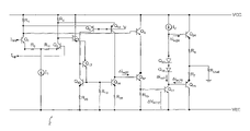
- the collector of bipolar transistor Q 5 is coupled to the voltage source VCC.
- the emitter of bipolar transistor Q 5 is coupled to the collector of bipolar transistor Q 12 .
- the emitter of pnp bipolar transistor Q 9 is coupled to the collector of bipolar transistor Q 1 , and the collector of bipolar transistor Q 9 is coupled to the base of bipolar transistor Q 12 and the collector of bipolar transistor Q 13 .
- the base of bipolar transistor Q 9 is coupled to a voltage source V and the base of bipolar transistor Q 10 .
- the emitter of bipolar transistor Q 12 is coupled to the bases of bipolar transistors Q 13 and Q 14 .
- the emitter of bipolar transistor Q 13 is coupled to a resistor R 23 .
- a resistor R 10 is coupled to bases of bipolar transistors Q 13 and Q 14 and to VEE.
- the emitter of bipolar transistor Q 14 is coupled to resistor R 26 . Both resistors R 23 and R 26 are also coupled to VEE.
- the emitter of a pnp bipolar transistor Q 10 is coupled to resistor R 2 .
- the collector of bipolar transistor Q 10 is coupled to the collector of bipolar transistor Q 14 .
- the collector of bipolar transistor Q 4 is coupled to the voltage source VCC, and the base of bipolar transistor Q 4 is coupled to the resistor R 1 .
- the emitter of bipolar transistor Q 4 is coupled to the collector of bipolar transistor Q 37 .
- the base of bipolar transistor Q 37 is coupled to the collector of bipolar transistor Q 14 , and the emitter of bipolar transistor Q 37 is coupled to a resistor R 15 , which is also coupled to VEE.
- the bipolar transistor Q 24 provides a change in the base current ( ⁇ i bq24 ) that does not match the change in the base current ( ⁇ i bq25 ) of the bipolar transistor Q 25 for a swing of the same magnitude in the negative direction.
- This nonlinearity change of current together with a changing current of the current source I 2 develops a nonlinear collector current ( ⁇ i cq17 ) through the bipolar transistor Q 17 .
- the ensuing voltage change between the base and emitter ( ⁇ V BE17 ) of the bipolar transistor Q 17 across resistor R 15 results in a nonlinear current through bipolar transistor Q 37 , which adds to the non-linear base current of bipolar transistor Q 17 . That error is reflected to one side of the differential input pair as a base current of the bipolar transistor Q 37 .
- the base current ( ⁇ i bq37 ) of the bipolar transistor Q 37 is replicated by the bipolar transistor Q 4 and fed to the opposite differential pair collector, thus creating a common mode error signal that can be easily rejected by the differential pair, out of an otherwise single current error that would cause a non-linear signal at the input of the amplifier.
- the circuit is particularly effective in reducing nonlinearities that grow larger with heavier loading since the base currents of the output devices increase as a function of load represented by the resistor Rload.
Landscapes
- Engineering & Computer Science (AREA)
- Power Engineering (AREA)
- Physics & Mathematics (AREA)
- Nonlinear Science (AREA)
- Amplifiers (AREA)
Abstract
Description
Claims (13)
Priority Applications (1)
| Application Number | Priority Date | Filing Date | Title |
|---|---|---|---|
| US12/103,153 US7679442B2 (en) | 2008-04-15 | 2008-04-15 | Output distortion cancellation circuit |
Applications Claiming Priority (1)
| Application Number | Priority Date | Filing Date | Title |
|---|---|---|---|
| US12/103,153 US7679442B2 (en) | 2008-04-15 | 2008-04-15 | Output distortion cancellation circuit |
Publications (2)
| Publication Number | Publication Date |
|---|---|
| US20090256634A1 US20090256634A1 (en) | 2009-10-15 |
| US7679442B2 true US7679442B2 (en) | 2010-03-16 |
Family
ID=41163486
Family Applications (1)
| Application Number | Title | Priority Date | Filing Date |
|---|---|---|---|
| US12/103,153 Active 2028-05-14 US7679442B2 (en) | 2008-04-15 | 2008-04-15 | Output distortion cancellation circuit |
Country Status (1)
| Country | Link |
|---|---|
| US (1) | US7679442B2 (en) |
Cited By (1)
| Publication number | Priority date | Publication date | Assignee | Title |
|---|---|---|---|---|
| US8907725B2 (en) | 2012-09-24 | 2014-12-09 | Analog Devices, Inc. | Circuit to prevent load-induced non-linearity in operational amplifiers |
Citations (1)
| Publication number | Priority date | Publication date | Assignee | Title |
|---|---|---|---|---|
| US5150074A (en) * | 1991-05-03 | 1992-09-22 | Analog Devices, Inc. | Wide-band transconductance generator |
-
2008
- 2008-04-15 US US12/103,153 patent/US7679442B2/en active Active
Patent Citations (1)
| Publication number | Priority date | Publication date | Assignee | Title |
|---|---|---|---|---|
| US5150074A (en) * | 1991-05-03 | 1992-09-22 | Analog Devices, Inc. | Wide-band transconductance generator |
Cited By (1)
| Publication number | Priority date | Publication date | Assignee | Title |
|---|---|---|---|---|
| US8907725B2 (en) | 2012-09-24 | 2014-12-09 | Analog Devices, Inc. | Circuit to prevent load-induced non-linearity in operational amplifiers |
Also Published As
| Publication number | Publication date |
|---|---|
| US20090256634A1 (en) | 2009-10-15 |
Similar Documents
| Publication | Publication Date | Title |
|---|---|---|
| US5907262A (en) | Folded-cascode amplifier stage | |
| US7298210B2 (en) | Fast settling, low noise, low offset operational amplifier and method | |
| US6489848B2 (en) | Linear and multi-sin h transconductance circuits | |
| JP3088262B2 (en) | Low distortion differential amplifier circuit | |
| US4748420A (en) | Quadcomp amplifier | |
| JP2005509347A (en) | Power amplifier with distortion compensation | |
| US6483382B1 (en) | Current compensation circuit for improved open-loop gain in an amplifier | |
| US7135927B2 (en) | Ultra fast, low noise operational amplifier with dynamic biasing | |
| US5825228A (en) | Low quiescent power, high output power rail-to rail amplifier output stages and methods for using same | |
| TWI647905B (en) | Pre-compensator for compensating the linearity of the amplifier | |
| US7250791B2 (en) | Current feedback amplifiers | |
| US5053718A (en) | Feedback control reducing signal distortion produced by differential amplifier stage | |
| US7471150B2 (en) | Class AB folded cascode stage and method for low noise, low power, low-offset operational amplifier | |
| US4068187A (en) | Audio-frequency power amplifiers | |
| US7679442B2 (en) | Output distortion cancellation circuit | |
| US20050007198A1 (en) | Power amplifier module | |
| JP3080488B2 (en) | Differential amplifier | |
| US9998080B2 (en) | Low voltage supply amplifier | |
| US6630866B2 (en) | High beta output stage for high speed operational amplifier | |
| US4972158A (en) | Transistor amplifier with variable bias circuits | |
| JPH04369105A (en) | Amplifier | |
| US6448853B1 (en) | Distortion improvement in amplifiers | |
| US4123723A (en) | Transistor amplifier circuit | |
| US9985589B2 (en) | System and method for improving total harmonic distortion of an amplifier | |
| US20060055460A1 (en) | Transimpedance amplifier with a high gain/bandwidth product for conversion of a DAC output current |
Legal Events
| Date | Code | Title | Description |
|---|---|---|---|
| AS | Assignment |
Owner name: ANALOG DEVICES, INC., MASSACHUSETTS Free format text: ASSIGNMENT OF ASSIGNORS INTEREST;ASSIGNORS:GERSTENHABER, MOSHE;BUNDOCK, JAMES;REEL/FRAME:021193/0221 Effective date: 20080702 Owner name: ANALOG DEVICES, INC.,MASSACHUSETTS Free format text: ASSIGNMENT OF ASSIGNORS INTEREST;ASSIGNORS:GERSTENHABER, MOSHE;BUNDOCK, JAMES;REEL/FRAME:021193/0221 Effective date: 20080702 |
|
| STCF | Information on status: patent grant |
Free format text: PATENTED CASE |
|
| FPAY | Fee payment |
Year of fee payment: 4 |
|
| MAFP | Maintenance fee payment |
Free format text: PAYMENT OF MAINTENANCE FEE, 8TH YEAR, LARGE ENTITY (ORIGINAL EVENT CODE: M1552) Year of fee payment: 8 |
|
| MAFP | Maintenance fee payment |
Free format text: PAYMENT OF MAINTENANCE FEE, 12TH YEAR, LARGE ENTITY (ORIGINAL EVENT CODE: M1553); ENTITY STATUS OF PATENT OWNER: LARGE ENTITY Year of fee payment: 12 |