US7640652B2 - Method of making a current sensing chip resistor - Google Patents

Method of making a current sensing chip resistor Download PDF

Info

Publication number
US7640652B2
US7640652B2 US11/703,835 US70383507A US7640652B2 US 7640652 B2 US7640652 B2 US 7640652B2 US 70383507 A US70383507 A US 70383507A US 7640652 B2 US7640652 B2 US 7640652B2
Authority
US
United States
Prior art keywords
resistor
aluminum nitride
nitride substrate
manufacturing process
layer
Prior art date
Legal status (The legal status is an assumption and is not a legal conclusion. Google has not performed a legal analysis and makes no representation as to the accuracy of the status listed.)
Expired - Fee Related, expires
Application number
US11/703,835
Other versions
US20080194057A1 (en
Inventor
Shen-Li Hsiao
Shih-Long Wei
Current Assignee (The listed assignees may be inaccurate. Google has not performed a legal analysis and makes no representation or warranty as to the accuracy of the list.)
Viking Tech Corp
Original Assignee
Viking Tech Corp
Priority date (The priority date is an assumption and is not a legal conclusion. Google has not performed a legal analysis and makes no representation as to the accuracy of the date listed.)
Filing date
Publication date
Application filed by Viking Tech Corp filed Critical Viking Tech Corp
Priority to US11/703,835 priority Critical patent/US7640652B2/en
Assigned to VIKING TECH CORPORATION reassignment VIKING TECH CORPORATION ASSIGNMENT OF ASSIGNORS INTEREST (SEE DOCUMENT FOR DETAILS). Assignors: HSIAO, SHEN-LI, WEI, SHIH-LONG
Publication of US20080194057A1 publication Critical patent/US20080194057A1/en
Application granted granted Critical
Publication of US7640652B2 publication Critical patent/US7640652B2/en
Expired - Fee Related legal-status Critical Current
Adjusted expiration legal-status Critical

Links

Images

Classifications

    • HELECTRICITY
    • H10SEMICONDUCTOR DEVICES; ELECTRIC SOLID-STATE DEVICES NOT OTHERWISE PROVIDED FOR
    • H10DINORGANIC ELECTRIC SEMICONDUCTOR DEVICES
    • H10D1/00Resistors, capacitors or inductors
    • H10D1/40Resistors
    • H10D1/47Resistors having no potential barriers
    • YGENERAL TAGGING OF NEW TECHNOLOGICAL DEVELOPMENTS; GENERAL TAGGING OF CROSS-SECTIONAL TECHNOLOGIES SPANNING OVER SEVERAL SECTIONS OF THE IPC; TECHNICAL SUBJECTS COVERED BY FORMER USPC CROSS-REFERENCE ART COLLECTIONS [XRACs] AND DIGESTS
    • Y10TECHNICAL SUBJECTS COVERED BY FORMER USPC
    • Y10TTECHNICAL SUBJECTS COVERED BY FORMER US CLASSIFICATION
    • Y10T29/00Metal working
    • Y10T29/49Method of mechanical manufacture
    • Y10T29/49002Electrical device making
    • Y10T29/49082Resistor making
    • Y10T29/49099Coating resistive material on a base

Definitions

  • the present invention relates to a method of making a current sensing chip resistor, and more particularly to a manufacturing method, wherein a thin-film process is utilized to make the resistor, and an aluminum nitride (AlN) substrate and a technique of a flip chip structure are used in the process.
  • AlN aluminum nitride
  • a conventional process A for making a resistor includes a rear-side conductor printing A 2 , a front-side resistor printing A 3 , a front-side conductor printing A 4 , a high-temperature baking A 5 , a glass protective layer printing A 6 , and a glass protective layer baking A 7 on an aluminum oxide (Al 2 O 3 ) substrate A 1 .
  • Al 2 O 3 aluminum oxide
  • the product will have a low power (1 W), a low precision (1%), a low conductivity, a high temperature coefficient, and a high noise.
  • the resistor manufacturing process A does not use a technique of a flip chip structure of a single-side manufacturing process; therefore, a problem of utilization space of a PCB (Printed Circuit Board) will be increased.
  • the primary object of present invention is to provide a method of making a current sensing chip resistor, wherein a thin-film process is utilized in the resistor manufacturing process, and an aluminum nitride (AlN) substrate and a technique of a flip chip structure is used in the process, such that the resistor can be provided with a high power, a high precision, a high thermal conductivity, and a utilization space of a PCB can be saved.
  • AlN aluminum nitride
  • FIG. 1 shows a block diagram of an implementation of a prior art.
  • FIG. 2 shows a first block diagram of an implementation of the present invention.
  • FIG. 3 shows a second block diagram of an implementation of the present invention.
  • FIG. 4 shows a first schematic view of an embodiment of the present invention.
  • FIG. 5 shows a second schematic view of an embodiment of the present invention.
  • FIG. 6 shows a third schematic view of an embodiment of the present invention.
  • FIG. 7 shows a fourth schematic view of an embodiment of the present invention.
  • FIG. 8 shows a fifth schematic view of an embodiment of the present invention.
  • FIG. 9 shows a sixth schematic view of an embodiment of the present invention.
  • FIG. 10 shows a seventh schematic view of an embodiment of the present invention.
  • FIG. 11 shows an eighth schematic view of an embodiment of the present invention.
  • FIG. 12 shows a first table of an embodiment of the present invention.
  • FIG. 13 shows a second table of an embodiment of the present invention.
  • a resistor manufacturing process B comprises a pre-process C and a post-process D.
  • a resistor mask layer coating C 2 is first performed on an aluminum nitride (AlN) substrate C 1 , followed by performing a resistor layer sputtering C 3 .
  • a resistor mask layer removal C 4 is performed on the aluminum nitride substrate C 1 , followed by performing a resistor protective layer coating C 5 , and then by performing a conductive layer plating C 6 on the aluminum nitride substrate C 1 .
  • a laser diode separation dicing C 7 is performed, and then the post-process D is proceeding.
  • a laser resistance dicing adjustment Dl is performed on the aluminum nitride substrate C 1 to adjust an accuracy of the resistance, and then a resistor protective layer printing D 2 is performed, followed by performing a marking printing D 3 on the aluminum nitride substrate C 1 .
  • a resistor protective layer baking-to-dry and hardening D 4 is performed, and then a primary cutting D 5 is performed on the aluminum nitride substrate C 1 .
  • a side conductor sputtering D 6 is performed on sides of the aluminum nitride substrate C 1 , followed by a secondary cutting D 7 .
  • a nickel layer plating D 8 is first performed on a surface of the aluminum nitride substrate C 1 , and then a tin layer plating D 9 is performed. After accomplishing the tin layer plating D 9 , a finished product of resistor is formed, which is then packaged D 10 to sell to users in need.
  • the resistor manufacturing process B includes respectively the pre-process C and the post-process D, the substrate material required in making the resistor is an aluminum nitride substrate E, and a thin-film process is used for the resistor manufacturing process B, in association with a technique of flip chip structure of a single-side manufacturing process. Accordingly, the resistor mask layer coating C 2 is first performed on the aluminum nitride substrate E, to coat a plurality of stripes of mask layer E 1 on a base E 2 of the aluminum nitride substrate E.
  • the resistor layer sputtering C 3 is then performed on the aluminum nitride substrate E, which coats a film layer on the base E 2 of the aluminum nitride substrate E.
  • the base E 2 of the aluminum nitride substrate E is provided with a resistor layer E 3 , and then the resistor mask layer C 4 is removed, which results in the base E 2 of the aluminum nitride substrate E after removing the mask layer E 1 .
  • the step of resistor protective layer coating C 5 is followed, to coat a plurality of stripes of protective layer E 4 on the aluminum nitride substrate E, and to form a grid pattern for the protective layer E 4 and the resistor layer E 3 on the aluminum nitride substrate E.
  • the conductive layer plating C 6 is performed to plate a conductive layer E 5 on the aluminum nitride substrate E, at positions where the protective layer E 4 is not printed.
  • the step of laser diode separation dicing C 7 is followed.
  • This laser diode separation dicing C 7 uses laser to dice on the aluminum nitride substrate E, to form cutting lines E 6 in a grid pattern on the aluminum nitride substrate E, followed by proceeding with the post-process D.
  • the laser resistance dicing adjustment is followed to adjust the resistance to an accurate value.
  • the resistor protective layer printing D 2 is performed, and then followed by the marking printing D 3 , which prints a marking E 7 on the protective layer E 4 of the aluminum nitride substrate E, thereby allowing a user to be aware of the resistance of this resistor.
  • the step of resistor protective layer baking-to-dry and hardening D 4 is performed, to bake dry the protective layer E 4 of the aluminum nitride substrate E at temperature of 220 ⁇ 10° C.
  • the primary cutting D 5 is performed on the aluminum nitride substrate E, which divides the cutting lines E 6 which are extended in a direction on the aluminum nitride substrate E to result in a semi-finished product E 8 .
  • the step of side conductor sputtering D 6 is followed, which sputters the conductive layer E 5 at sides of the semi-finished product E 8 , so as to facilitate the user to easily weld and conduct a PCB.
  • the secondary cutting D 7 is followed, which divides the cutting lines E 6 which are extended along the other direction on the semi-finished product E 8 , to result in a resistor E 10 .
  • the nickel layer plating D 8 and the tin layer plating D 9 are followed, to plate nickel and tin on a surface E 9 of the resistor E 10 , thereby accomplishing the manufacturing of the resistor E 10 , and enabling a packaging to the finished resistor product D 10 .
  • the thin-film process is utilized, and the aluminum nitride substrate C 1 and the technique of flip chip structure of the single-side manufacturing process are employed, so as to achieve performances of a high power (>2 W), a high precision ( ⁇ 0.5%), a high thermal conductivity (150 ⁇ 230 mW), and a saving of utilization space of the PCB (30%).

Landscapes

  • Apparatuses And Processes For Manufacturing Resistors (AREA)

Abstract

A method of making a current sensing chip resistor is composed of a resistor manufacturing process which is constituted by a pre-process and a post-process. In addition, a thin-film process is used for the resistor manufacturing process, and the aluminum nitride substrate is used in the thin-film, in association with a technique of flip chip structure of single-side manufacturing process, enabling the resistor to be provided with performances of a high power, a high precision, a high thermal conductivity, a low temperature coefficient, a low noise, and a saving of utilization space of PCB (Printed Circuit Board).

Description

BACKGROUND OF THE INVENTION
(a) Field of the Invention
The present invention relates to a method of making a current sensing chip resistor, and more particularly to a manufacturing method, wherein a thin-film process is utilized to make the resistor, and an aluminum nitride (AlN) substrate and a technique of a flip chip structure are used in the process.
(b) Description of the Prior Art
Referring to FIG. 1, a conventional process A for making a resistor includes a rear-side conductor printing A2, a front-side resistor printing A3, a front-side conductor printing A4, a high-temperature baking A5, a glass protective layer printing A6, and a glass protective layer baking A7 on an aluminum oxide (Al2O3) substrate A1. However, as the aluminum oxide substrate A1 is used in a pre-process, and only a thick-film process is used for the resistor manufacturing process A, the product will have a low power (1 W), a low precision (1%), a low conductivity, a high temperature coefficient, and a high noise. In addition, the resistor manufacturing process A does not use a technique of a flip chip structure of a single-side manufacturing process; therefore, a problem of utilization space of a PCB (Printed Circuit Board) will be increased.
Therefore, how to eliminate the aforementioned shortcomings is a technical issue to be solved by the present inventor.
SUMMARY OF THE INVENTION
The primary object of present invention is to provide a method of making a current sensing chip resistor, wherein a thin-film process is utilized in the resistor manufacturing process, and an aluminum nitride (AlN) substrate and a technique of a flip chip structure is used in the process, such that the resistor can be provided with a high power, a high precision, a high thermal conductivity, and a utilization space of a PCB can be saved.
To enable a further understanding of the said objectives and the technological methods of the invention herein, the brief description of the drawings below is followed by the detailed description of the preferred embodiments.
BRIEF DESCRIPTION OF THE DRAWINGS
FIG. 1 shows a block diagram of an implementation of a prior art.
FIG. 2 shows a first block diagram of an implementation of the present invention.
FIG. 3 shows a second block diagram of an implementation of the present invention.
FIG. 4 shows a first schematic view of an embodiment of the present invention.
FIG. 5 shows a second schematic view of an embodiment of the present invention.
FIG. 6 shows a third schematic view of an embodiment of the present invention.
FIG. 7 shows a fourth schematic view of an embodiment of the present invention.
FIG. 8 shows a fifth schematic view of an embodiment of the present invention.
FIG. 9 shows a sixth schematic view of an embodiment of the present invention.
FIG. 10 shows a seventh schematic view of an embodiment of the present invention.
FIG. 11 shows an eighth schematic view of an embodiment of the present invention.
FIG. 12 shows a first table of an embodiment of the present invention.
FIG. 13 shows a second table of an embodiment of the present invention.
DETAILED DESCRIPTION OF THE PREFERRED EMBODIMENTS
The present invention is to provide a method of making a current sensing chip resistor. Referring to FIG. 2 and FIG. 3, a resistor manufacturing process B comprises a pre-process C and a post-process D. For the pre-process C, a resistor mask layer coating C2 is first performed on an aluminum nitride (AlN) substrate C1, followed by performing a resistor layer sputtering C3. Next, a resistor mask layer removal C4 is performed on the aluminum nitride substrate C1, followed by performing a resistor protective layer coating C5, and then by performing a conductive layer plating C6 on the aluminum nitride substrate C1. Finally, a laser diode separation dicing C7 is performed, and then the post-process D is proceeding.
For the post-process D, a laser resistance dicing adjustment Dl is performed on the aluminum nitride substrate C1 to adjust an accuracy of the resistance, and then a resistor protective layer printing D2 is performed, followed by performing a marking printing D3 on the aluminum nitride substrate C1. After accomplishing the marking printing D3, a resistor protective layer baking-to-dry and hardening D4 is performed, and then a primary cutting D5 is performed on the aluminum nitride substrate C1. Next, a side conductor sputtering D6 is performed on sides of the aluminum nitride substrate C1, followed by a secondary cutting D7. After that, a nickel layer plating D8 is first performed on a surface of the aluminum nitride substrate C1, and then a tin layer plating D9 is performed. After accomplishing the tin layer plating D9, a finished product of resistor is formed, which is then packaged D10 to sell to users in need.
Referring to FIGS. 3 to 5, the resistor manufacturing process B includes respectively the pre-process C and the post-process D, the substrate material required in making the resistor is an aluminum nitride substrate E, and a thin-film process is used for the resistor manufacturing process B, in association with a technique of flip chip structure of a single-side manufacturing process. Accordingly, the resistor mask layer coating C2 is first performed on the aluminum nitride substrate E, to coat a plurality of stripes of mask layer E1 on a base E2 of the aluminum nitride substrate E. As the mask layer E1 of the base E2 is not conductive, the resistor layer sputtering C3 is then performed on the aluminum nitride substrate E, which coats a film layer on the base E2 of the aluminum nitride substrate E. After coating on the aluminum nitride substrate E, the base E2 of the aluminum nitride substrate E is provided with a resistor layer E3, and then the resistor mask layer C4 is removed, which results in the base E2 of the aluminum nitride substrate E after removing the mask layer E1.
Referring to FIG. 3, FIG. 6, and FIG. 7, after accomplishing the resistor mask layer removal C4 on the aluminum nitride substrate E, the step of resistor protective layer coating C5 is followed, to coat a plurality of stripes of protective layer E4 on the aluminum nitride substrate E, and to form a grid pattern for the protective layer E4 and the resistor layer E3 on the aluminum nitride substrate E. After accomplishing the resistor protective layer coating C5, the conductive layer plating C6 is performed to plate a conductive layer E5 on the aluminum nitride substrate E, at positions where the protective layer E4 is not printed.
Referring to FIG. 3, FIG. 8, and FIG. 9, after accomplishing the conductive layer plating C6 on the aluminum nitride substrate E, the step of laser diode separation dicing C7 is followed. This laser diode separation dicing C7 uses laser to dice on the aluminum nitride substrate E, to form cutting lines E6 in a grid pattern on the aluminum nitride substrate E, followed by proceeding with the post-process D. When the laser diode separation dicing C7 is accomplished, the laser resistance dicing adjustment is followed to adjust the resistance to an accurate value. After accomplishing the laser resistance dicing adjustment D1, the resistor protective layer printing D2 is performed, and then followed by the marking printing D3, which prints a marking E7 on the protective layer E4 of the aluminum nitride substrate E, thereby allowing a user to be aware of the resistance of this resistor. After accomplishing the marking printing D3, the step of resistor protective layer baking-to-dry and hardening D4 is performed, to bake dry the protective layer E4 of the aluminum nitride substrate E at temperature of 220±10° C.
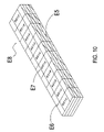
Referring to FIG. 3, FIG. 10, and FIG. 11, after accomplishing the resistor protective layer baking-to-dry and hardening D4, the primary cutting D5 is performed on the aluminum nitride substrate E, which divides the cutting lines E6 which are extended in a direction on the aluminum nitride substrate E to result in a semi-finished product E8. After performing the primary cutting D5, the step of side conductor sputtering D6 is followed, which sputters the conductive layer E5 at sides of the semi-finished product E8, so as to facilitate the user to easily weld and conduct a PCB. After accomplishing the side conductor sputtering D6, the secondary cutting D7 is followed, which divides the cutting lines E6 which are extended along the other direction on the semi-finished product E8, to result in a resistor E10. After accomplishing the secondary cutting D7, the nickel layer plating D8 and the tin layer plating D9 are followed, to plate nickel and tin on a surface E9 of the resistor E10, thereby accomplishing the manufacturing of the resistor E10, and enabling a packaging to the finished resistor product D10.
Referring to FIG. 3, FIG. 11, FIG. 12, and FIG. 13, when making the resistor E10, the thin-film process is utilized, and the aluminum nitride substrate C1 and the technique of flip chip structure of the single-side manufacturing process are employed, so as to achieve performances of a high power (>2 W), a high precision (≦0.5%), a high thermal conductivity (150˜230 mW), and a saving of utilization space of the PCB (30%).
To further manifest the advancement and practicability of the present invention, the advantages thereof are listed as follow:
    • 1. The aluminum nitride substrate, thin-film process, and flip chip structure of the single-side manufacturing process are used.
    • 2. According to item 1, the performance of high power (>2 W) can be resulted.
    • 3. According to item 1, the performance of high precision (≦0.5%) can be resulted.
    • 4. According to item 1, the performance of high thermal conductivity (150˜230 mW) can be resulted.
    • 5. According to item 1, the saving of utilization of PCB (30%) can be achieved.
    • 6. It is provided with industrial competitiveness.
    • 7. It is provided with a value of business utilization.
    • 8. It is provided with novelty.
It is of course to be understood that the embodiments described herein is merely illustrative of the principles of the invention and that a wide variety of modifications thereto may be effected by persons skilled in the art without departing from the spirit and scope of the invention as set forth in the following claims.

Claims (1)

1. A method of making a current sensing chip resistor, comprising a resistor manufacturing process comprised of a pre-process and a post-process,
wherein the pre-process further comprises the following sequential steps:
performing a resistor mask layer coating on an aluminum nitride substrate;
performing a resistor layer sputtering;
removing a resistor mask layer;
performing a resistor protective layer coating;
performing a conductive layer plating on the aluminum nitride substrate;
performing a laser diode separation dicing;
performing the post-processing, the post processing comprising the following sequential steps:
performing a laser resistance dicing adjustment to adjust the accuracy of the resistance;
performing a resistor protective layer printing;
performing a marking printing;
performing a resistor protective layer baking-to-dry and hardening;
performing a primary cutting on the aluminum nitride substrate;
performing a side conductor sputtering;
performing a secondary cutting;
performing a nickel layer plating;
performing a tin layer plating; and
packaging the apparatus,
wherein a thin-film process is used for the resistor manufacturing process and the aluminum nitride substrate,
wherein the thin-film process uses a single-side flip chip structure manufacturing process.
US11/703,835 2007-02-08 2007-02-08 Method of making a current sensing chip resistor Expired - Fee Related US7640652B2 (en)

Priority Applications (1)

Application Number Priority Date Filing Date Title
US11/703,835 US7640652B2 (en) 2007-02-08 2007-02-08 Method of making a current sensing chip resistor

Applications Claiming Priority (1)

Application Number Priority Date Filing Date Title
US11/703,835 US7640652B2 (en) 2007-02-08 2007-02-08 Method of making a current sensing chip resistor

Publications (2)

Publication Number Publication Date
US20080194057A1 US20080194057A1 (en) 2008-08-14
US7640652B2 true US7640652B2 (en) 2010-01-05

Family

ID=39686183

Family Applications (1)

Application Number Title Priority Date Filing Date
US11/703,835 Expired - Fee Related US7640652B2 (en) 2007-02-08 2007-02-08 Method of making a current sensing chip resistor

Country Status (1)

Country Link
US (1) US7640652B2 (en)

Citations (5)

* Cited by examiner, † Cited by third party
Publication number Priority date Publication date Assignee Title
US20020026706A1 (en) * 2000-08-10 2002-03-07 Yoshio Kurita Method of making chip resistor
US20020118094A1 (en) * 1999-07-30 2002-08-29 Shigeru Kambara Chip resistor and method of making the same
US6492896B2 (en) * 2000-07-10 2002-12-10 Rohm Co., Ltd. Chip resistor
US20030156008A1 (en) * 2001-03-01 2003-08-21 Tsutomu Nakanishi Resistor
US20040075717A1 (en) * 2002-10-16 2004-04-22 O'brien Seamus Wafer processing apparatus and method

Patent Citations (5)

* Cited by examiner, † Cited by third party
Publication number Priority date Publication date Assignee Title
US20020118094A1 (en) * 1999-07-30 2002-08-29 Shigeru Kambara Chip resistor and method of making the same
US6492896B2 (en) * 2000-07-10 2002-12-10 Rohm Co., Ltd. Chip resistor
US20020026706A1 (en) * 2000-08-10 2002-03-07 Yoshio Kurita Method of making chip resistor
US20030156008A1 (en) * 2001-03-01 2003-08-21 Tsutomu Nakanishi Resistor
US20040075717A1 (en) * 2002-10-16 2004-04-22 O'brien Seamus Wafer processing apparatus and method

Also Published As

Publication number Publication date
US20080194057A1 (en) 2008-08-14

Similar Documents

Publication Publication Date Title
US8242878B2 (en) Resistor and method for making same
US8994491B2 (en) Chip resistor and method of manufacturing the same
CN105374480A (en) High-power chip whole-film fixed resistor and production method thereof
CN106898448A (en) Chip resistor and its manufacture method
CN100524547C (en) Method for manufacturing current sensing chip resistor
US7640652B2 (en) Method of making a current sensing chip resistor
JP2014116456A (en) Chip resistor, current sensor device, and manufacturing method of chip resistor
JP5499518B2 (en) Method for manufacturing thin film chip resistor
CN109830351B (en) Chip resistor and processing method thereof
CN103400674B (en) The manufacture method of ultrathin alloy plate sensitive resistor
CN206725638U (en) The terminal current sensing component of noncontinuous electrode four
JP5042420B2 (en) Manufacturing method of chip resistor
CN109324219A (en) Short-electrode four-terminal current sensing component and its production process
CN109326400A (en) A current detection resistor and its manufacturing process
JP2001307903A (en) Manufacturing method of thin film resistor
JP3196519B2 (en) Method of manufacturing rectangular thin film chip resistor
JP3304130B2 (en) Method of manufacturing rectangular thin film chip resistor
WO2012039020A1 (en) Method for producing metal plate low-resistance chip resistor
CN110246640A (en) A kind of hurtless measure resistance value method for repairing and regulating
JP2006019323A (en) Resistance composition, chip resistor and their manufacturing method
CN206181536U (en) Ceramic substrate convenient to discernment
US20250140450A1 (en) Chip resistor
JP3766663B2 (en) Manufacturing method of chip parts
JP2002056767A (en) Chip type fuse and its narrow fusing section forming method
TWI566261B (en) Thick film chip resistor

Legal Events

Date Code Title Description
AS Assignment

Owner name: VIKING TECH CORPORATION, TAIWAN

Free format text: ASSIGNMENT OF ASSIGNORS INTEREST;ASSIGNORS:HSIAO, SHEN-LI;WEI, SHIH-LONG;REEL/FRAME:018978/0805

Effective date: 20070108

FPAY Fee payment

Year of fee payment: 4

FEPP Fee payment procedure

Free format text: MAINTENANCE FEE REMINDER MAILED (ORIGINAL EVENT CODE: REM.)

LAPS Lapse for failure to pay maintenance fees

Free format text: PATENT EXPIRED FOR FAILURE TO PAY MAINTENANCE FEES (ORIGINAL EVENT CODE: EXP.)

STCH Information on status: patent discontinuation

Free format text: PATENT EXPIRED DUE TO NONPAYMENT OF MAINTENANCE FEES UNDER 37 CFR 1.362

FP Lapsed due to failure to pay maintenance fee

Effective date: 20180105