US7638248B2 - Electrophotographic photoconductor - Google Patents
Electrophotographic photoconductor Download PDFInfo
- Publication number
- US7638248B2 US7638248B2 US11/593,504 US59350406A US7638248B2 US 7638248 B2 US7638248 B2 US 7638248B2 US 59350406 A US59350406 A US 59350406A US 7638248 B2 US7638248 B2 US 7638248B2
- Authority
- US
- United States
- Prior art keywords
- electrophotographic photoconductor
- charge transporting
- photoconductor
- image
- layer
- Prior art date
- Legal status (The legal status is an assumption and is not a legal conclusion. Google has not performed a legal analysis and makes no representation as to the accuracy of the status listed.)
- Expired - Fee Related, expires
Links
Images


Classifications
-
- G—PHYSICS
- G03—PHOTOGRAPHY; CINEMATOGRAPHY; ANALOGOUS TECHNIQUES USING WAVES OTHER THAN OPTICAL WAVES; ELECTROGRAPHY; HOLOGRAPHY
- G03G—ELECTROGRAPHY; ELECTROPHOTOGRAPHY; MAGNETOGRAPHY
- G03G5/00—Recording members for original recording by exposure, e.g. to light, to heat, to electrons; Manufacture thereof; Selection of materials therefor
- G03G5/02—Charge-receiving layers
- G03G5/04—Photoconductive layers; Charge-generation layers or charge-transporting layers; Additives therefor; Binders therefor
- G03G5/05—Organic bonding materials; Methods for coating a substrate with a photoconductive layer; Inert supplements for use in photoconductive layers
- G03G5/0528—Macromolecular bonding materials
- G03G5/0557—Macromolecular bonding materials obtained otherwise than by reactions only involving carbon-to-carbon unsatured bonds
- G03G5/0564—Polycarbonates
-
- G—PHYSICS
- G03—PHOTOGRAPHY; CINEMATOGRAPHY; ANALOGOUS TECHNIQUES USING WAVES OTHER THAN OPTICAL WAVES; ELECTROGRAPHY; HOLOGRAPHY
- G03G—ELECTROGRAPHY; ELECTROPHOTOGRAPHY; MAGNETOGRAPHY
- G03G5/00—Recording members for original recording by exposure, e.g. to light, to heat, to electrons; Manufacture thereof; Selection of materials therefor
- G03G5/02—Charge-receiving layers
- G03G5/04—Photoconductive layers; Charge-generation layers or charge-transporting layers; Additives therefor; Binders therefor
- G03G5/043—Photoconductive layers characterised by having two or more layers or characterised by their composite structure
- G03G5/047—Photoconductive layers characterised by having two or more layers or characterised by their composite structure characterised by the charge-generation layers or charge transport layers
-
- G—PHYSICS
- G03—PHOTOGRAPHY; CINEMATOGRAPHY; ANALOGOUS TECHNIQUES USING WAVES OTHER THAN OPTICAL WAVES; ELECTROGRAPHY; HOLOGRAPHY
- G03G—ELECTROGRAPHY; ELECTROPHOTOGRAPHY; MAGNETOGRAPHY
- G03G5/00—Recording members for original recording by exposure, e.g. to light, to heat, to electrons; Manufacture thereof; Selection of materials therefor
- G03G5/02—Charge-receiving layers
- G03G5/04—Photoconductive layers; Charge-generation layers or charge-transporting layers; Additives therefor; Binders therefor
- G03G5/06—Photoconductive layers; Charge-generation layers or charge-transporting layers; Additives therefor; Binders therefor characterised by the photoconductive material being organic
- G03G5/0601—Acyclic or carbocyclic compounds
- G03G5/0612—Acyclic or carbocyclic compounds containing nitrogen
- G03G5/0614—Amines
- G03G5/06142—Amines arylamine
- G03G5/06147—Amines arylamine alkenylarylamine
- G03G5/061473—Amines arylamine alkenylarylamine plural alkenyl groups linked directly to the same aryl group
-
- G—PHYSICS
- G03—PHOTOGRAPHY; CINEMATOGRAPHY; ANALOGOUS TECHNIQUES USING WAVES OTHER THAN OPTICAL WAVES; ELECTROGRAPHY; HOLOGRAPHY
- G03G—ELECTROGRAPHY; ELECTROPHOTOGRAPHY; MAGNETOGRAPHY
- G03G5/00—Recording members for original recording by exposure, e.g. to light, to heat, to electrons; Manufacture thereof; Selection of materials therefor
- G03G5/02—Charge-receiving layers
- G03G5/04—Photoconductive layers; Charge-generation layers or charge-transporting layers; Additives therefor; Binders therefor
- G03G5/06—Photoconductive layers; Charge-generation layers or charge-transporting layers; Additives therefor; Binders therefor characterised by the photoconductive material being organic
- G03G5/0601—Acyclic or carbocyclic compounds
- G03G5/0612—Acyclic or carbocyclic compounds containing nitrogen
- G03G5/0614—Amines
- G03G5/06149—Amines enamine
-
- G—PHYSICS
- G03—PHOTOGRAPHY; CINEMATOGRAPHY; ANALOGOUS TECHNIQUES USING WAVES OTHER THAN OPTICAL WAVES; ELECTROGRAPHY; HOLOGRAPHY
- G03G—ELECTROGRAPHY; ELECTROPHOTOGRAPHY; MAGNETOGRAPHY
- G03G5/00—Recording members for original recording by exposure, e.g. to light, to heat, to electrons; Manufacture thereof; Selection of materials therefor
- G03G5/02—Charge-receiving layers
- G03G5/04—Photoconductive layers; Charge-generation layers or charge-transporting layers; Additives therefor; Binders therefor
- G03G5/06—Photoconductive layers; Charge-generation layers or charge-transporting layers; Additives therefor; Binders therefor characterised by the photoconductive material being organic
- G03G5/0664—Dyes
- G03G5/0666—Dyes containing a methine or polymethine group
- G03G5/0672—Dyes containing a methine or polymethine group containing two or more methine or polymethine groups
-
- G—PHYSICS
- G03—PHOTOGRAPHY; CINEMATOGRAPHY; ANALOGOUS TECHNIQUES USING WAVES OTHER THAN OPTICAL WAVES; ELECTROGRAPHY; HOLOGRAPHY
- G03G—ELECTROGRAPHY; ELECTROPHOTOGRAPHY; MAGNETOGRAPHY
- G03G5/00—Recording members for original recording by exposure, e.g. to light, to heat, to electrons; Manufacture thereof; Selection of materials therefor
- G03G5/14—Inert intermediate or cover layers for charge-receiving layers
- G03G5/147—Cover layers
- G03G5/14708—Cover layers comprising organic material
- G03G5/14713—Macromolecular material
- G03G5/14747—Macromolecular material obtained otherwise than by reactions only involving carbon-to-carbon unsaturated bonds
- G03G5/14756—Polycarbonates
Definitions
- the invention relates to an electrophotographic photoconductor to be used for image formation by electrophotography and an image forming apparatus provided with the electrophotographic photoconductor.
- An electrophotographic image forming apparatus to be used for a copying machine, a printer, a facsimile apparatus (hereinafter, referred to as electrophotographic apparatus in some cases) or the like forms an image through the following electrophotographic process.
- a photosensitive layer of an electrophotographic photoconductor (hereinafter, simply referred to as photoconductor in some cases) installed in the apparatus is evenly charged at a prescribed potential by an electric charger and exposed to light such as laser beam radiated by exposure means corresponding to image information to form an electrostatic latent image.
- a developer is supplied to the formed electrostatic latent image from development means for depositing colored fine particles called as a toner, which is a component of the developer, on the surface of the photoconductor to develop the electrostatic latent image and visualize a toner image. Further, the formed toner image is transferred onto a transfer material such as recording paper from the surface of the photoconductor by transfer means and fixed by fixing means.
- a transfer material such as recording paper
- the toner on the photoconductor surface is not necessarily entirely transferred and shifted to the recording paper, but partially remains on the photoconductor surface or the paper powder of the recording paper brought into contact with the photoconductor at the time of transfer may remain while being stuck to the photoconductor surface.
- the remaining toner and the foreign substances such as the adhering paper powder on the photoconductor surface cause a bad effect on the quality of an image to be formed and therefore they are removed by a cleaning apparatus.
- the electrophotographic photoconductor to be used in such electrophotographic process is composed by layering a photosensitive layer containing photoconductive material on a conductive substrate made of a conductive material.
- an electrophotographic photoconductor using an inorganic photoconductive material hereinafter, referred to as inorganic photoconductor.
- Typical examples of the inorganic photoconductor are selenium type photoconductors having a photoconductive layer containing such as amorphous selenium (a-Se) or an amorphous selenium-arsenic (a-AsSe); zinc oxide type or cadmium sulfide type photoconductors having a photoconductive layer containing zinc oxide (ZnO) or cadmium sulfide (CdS) dispersed together with a sensitizer such as a coloring material in a resin; and amorphous silicon type photoconductors, having a photoconductive layer containing amorphous silicon (a-Si) (hereinafter, referred to as a-Si photoconductor).
- a-Se amorphous selenium
- a-AsSe amorphous selenium-arsenic
- ZnO zinc oxide
- CdS cadmium sulfide
- a-Si photoconductor a
- the inorganic photoconductor has the following disadvantageous points. That is, the selenium type photoconductors and the cadmium sulfide type photoconductors are problematic in the heat resistance and storage stability. Further, selenium and cadmium are toxic to living things including human being and their use is a problem in terms of the environmental pollution and therefore, it is required to collect the photoconductors using them and to properly dispose them after use. Moreover, the zinc oxide type photoconductors are disadvantageously less sensitive and inferior in durability and therefore, they are scarcely used today.
- the a-Si photoconductors drawing attention as an environment-friendly inorganic photoconductor are advantageous having high sensitivity and good durability, however since they are disadvantageously produced by a plasma chemical vapor deposition method, it is difficult to evenly form a photosensitive-layer and image defects are easily caused. Further, the a-Si photoconductors are inferior in the productivity and thus the production cost is disadvantageously high.
- inorganic photoconductors have many disadvantageous points, it has been required to develop new photoconductive materials to be used for the electrophotographic photoconductor and accordingly an organic type photoconductive material, that is an organic photoconductor (Organic Photoconductor: abbreviated OPC), has been often used in place of the conventionally used inorganic type photoconductive material.
- organic photoconductor Organic Photoconductor: abbreviated OPC
- organic photoconductor The electrophotographic photoconductor using an organic type photoconductive material (hereinafter, referred to as organic photoconductor) is rather much advantageous as compared with the inorganic photoconductor in terms of toxicity, production cost, and option of the material planning although having slight problems in the sensitivity, durability, and environmental stability. Further, the organic photoconductor has an advantageous point that its photoconductive layer can be formed by an easy and economical method, for example, by an immersion coating method.
- the organic photoconductor tends to be used dominantly for the electrophotographic photoconductor. Further based on the recent investigations and developments, the sensitivity and durability of the organic photoconductor have been improved and today the organic photoconductor has been used for the electrophotographic photoconductor, except special cases.
- the capability of the organic photoconductor has been remarkably improved by development of a function-separation type photoconductor in which the charge generating function and the charge transporting function are allotted to respectively different substances. That is, the function-separation type photoconductor has an advantageous point in addition to the above-mentioned advantages of the organic photoconductor that the option of selecting materials composing the photoconductive layer is wide and that the production of a photoconductor having desired characteristics is relatively easy.
- This function-separation type photoconductor is classified into a layered type and a monolayer type and in a layered type function-separation photoconductor, a layered type photoconductive layer composed of a charge generating layer containing a charge generating substance to which the charge generating function is allotted and a charge transporting layer containing a charge transporting substance to which the charge transporting function is allotted.
- the above-mentioned charge generating layer and charge transporting layer are, in general, formed by dispersing the charge generating substance and the charge transporting substance respectively in binder resins, which are binders.
- the monolayer type function-separation photoconductor has a monolayer type photoconductive layer formed by dispersing the charge generating substance and the charge transporting substance together in a binder resin.
- the charge generating substance to be used for the function-separation type photoconductor have been investigated many kinds of substances such as phthalocyanine pigments, squarylium coloring materials, azo pigments, perylene pigments, polycyclic quinone pigments, cyanine coloring materials, squaric acid dyes, and pyrylium type coloring materials and various kinds of materials with high light fastness and high charge generating capability have been proposed.
- pyrazoline compounds As the charge transporting substance have been developed pyrazoline compounds, hydrazone compounds, triphenylamine compounds, stilbene compounds and moreover, in recent years, pyrene derivatives, naphthalene derivatives, and terphenyl derivatives having condensed polycyclic hydrocarbons as a center mother skeletone have been developed.
- a charge transporting substance is required
- the photoconductor has been required to have high sensitivity as a photoconductor characteristic and the charge transporting substance is required to have particularly high charge transporting capability corresponding to the demands for miniaturization and high speed to electrophotographic apparatus such as digital copying machines and printers. Further in the high speed electrophotographic process, since the time from exposure to development is short, it is required for the photoconductor to be excellent in the photo-response.
- the photo-response of the photoconductor is low, that is, if the decaying speed of the surface potential after the exposure is slow, the remaining potential rises and the photoconductor is used repeatedly in the state that the surface potential is not sufficiently decayed and the surface charge to be removed is not sufficiently eliminated by the exposure to result in undesirable consequence such as early deterioration of the quality of images.
- the charge generated in the charge generating substance by light absorption is transported to the photosensitive layer surface by the charge transporting substance and the surface charge in the portion of the photoconductor radiated with light is removed, so that the photo-response depends on the charge transporting capacity of the charge transporting substance. Accordingly, also in terms of actualization of a photoconductor having sufficient photo-response, the charge transporting substance is required to have high charge transporting capability.
- the photoconductor In actual use of an electrophotographic apparatus, since the above-mentioned operations of charging, exposure, development, transfer, cleaning, and static elimination are repeated for the photoconductor under various conditions, the photoconductor is required to have environmental stability, electric stability, and durability to external mechanical force in addition to the high sensitivity and excellent photo-response.
- the photoconductor it is required for the photoconductor to have a surface layer hard to be abraded by sliding and friction with a cleaning member or the like. Accordingly, it is made possible to provide a photoconductor excellent in high durability to printing by specifying physical properties of the photoconductor surface satisfying the above-mentioned aims.
- Hardness is one of indexes for evaluation of the physical properties of a wide range of materials including the electrophotographic photoconductor surface, particularly for evaluation of mechanical properties. Hardness is defined as the stress of a material when a presser is pushed into the material. It is tried to quantify a mechanical property of a film composing the electrophotographic photoconductor surface by using the hardness as a physical parameter informing the physical property of a material. For example, a scratching strength test, a pencil hardness test, and a Vickers hardness test have been known well as a testing method for measuring the hardness. However, in any hardness test, there are problems in measurements of mechanical properties of a material showing complicated behaviors such as plasticity, elasticity (including delay component) as a film containing an organic matter, or the like.
- Vickers hardness test evaluates the hardness by measuring the length of the pressed trace in a film, however it reflects only the plasticity of the film and it cannot precisely evaluate a mechanical property of organic matter which may be deformed at a high elastic deformation ratio. Accordingly, mechanical properties of a film made of organic matter have to be evaluated in consideration of various characteristics.
- plastic power plastic deformation ratio, ⁇ plast , %) and elastic power (elastic deformation ratio, ⁇ HU , %) are described as the physical properties to be used for judgment of long term abrasion resistance, durability, and operational stability (e.g. reference to JP 2000-10320 and JP 2002-6526).
- the plastic power is a percentage of the ratio of the plastic deformation workload to the total of the plastic deformation workload (energy required for the plastic deformation) and the elastic workload (energy required for the elastic deformation).
- the elastic power is a percentage of the ratio of the elastic deformation workload to the total of the plastic deformation workload and the elastic workload.
- the total of the plastic power and the elastic power becomes 100 (%).
- JP 2000-10320 practically describes that the plastic power (plastic deformation ratio) is set to be in a range from 30 to 70% and that the universal hardness (Hu) measured by a universal hardness test standardized in DIN50359-1 is set in a range from 230 to 700 N/mm 2 . Further, the Document No. 5 describes that such setting in the numerical range prevents mechanical deterioration of the photoconductor surface layer.
- the numerical range of the plastic power from 30 to 70% is a range covering almost all of organic photosensitive layers containing binder resins used commonly today. Accordingly, even if the plastic power is in the above-mentioned range, it is not necessarily always possible to obtain an organic photosensitive layer excellent in long term abrasion resistance, durability, and operation stability.
- the numeral value of 32 to 60% for the elastic power means the same as that the plastic power is in a range from 40 to 68% and similarly to JP 2000-10320, it covers almost all of electrophotographic photoconductors having an organic photosensitive layer as the surface layer which have been used today.
- curable resin to be used as the binder resin is also common in technical fields of electrophotographic photoconductors.
- JP 2002-6526 does not practically describe the solution means of obtaining an organic photosensitive layer excellent in long term abrasion resistance, durability, and operation stability. Further, the electrophotographic photoconductor of JP 2002-6526 has a problem that formation of the protection layer containing the curable resin leads to the cost up.
- a polyarylate type resin described in JP 2004-219922 is disclosed to have a type of resin excellent in exhibition of high printing durability, however in terms of the solubility, it is indispensable to use a halogenated benzene such as monochlorobenzene and a specified halogen type organic solvent and in terms of the effect on the health of human being and global environmental preservation, it cannot be denied that the production is limited considerably.
- an aim of the invention is to solve the problem and provide a photoconductor usable for a long term.
- an electrophotographic photoconductor which is obtained by successively layering at least a charge generating layer and a charge transporting layer containing a binder resin and a charge transporting material on a conductive substrate and of which the charge transporting layer have a layered structure composed of a plurality of charge transporting layers of which the outermost charge transporting layer of the electrophotographic photoconductor has elastic power ( ⁇ HU ) and hardness value of plastic deformation respectively specified ranges in the surface coating hardness test, and these findings have now led to completion of the invention.
- the invention provides an electrophotographic photoconductor comprising a conductive substrate and at least a charge generating layer and a charge transporting layer successively layered on the substrate, wherein the charge transporting layer comprises a charge transporting material (M) and a binder resin (B) which contains, as a main component, a compound represented by the general formula (1):
- the invention provides an electrophotographic photoconductor as described above, in which the charge transporting layer contains a charge transporting material having an enamine structure represented by the following formula (2).
- the invention provides an image forming apparatus comprising the above-mentioned electrophotographic photoconductor, charging means for charging the electrophotographic photoconductor, exposure means for exposing the charged electrophotographic photoconductor to light corresponding to the image information for forming an electrostatic latent image, development means for developing a toner image by developing the electrostatic latent image, transfer means for transferring the toner image to a transfer material from the surface of the electrophotographic photoconductor, and cleaning means for cleaning the surface of the electrophotographic photoconductor after the transfer of the toner image.
- an electrophotographic photoconductor excellent in both of the electric properties and printing durability and maintaining high durability for a long time can be obtained.
- the electrophotographic photoconductor makes it possible to miniaturize a copying machine and a printer, carry out image formation stably for a long duration, and provide an image formation apparatus at a low cost without requiring frequent maintenance.
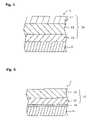
- FIG. 1 is a partial cross-sectional view showing a simplified configuration of an electrophotographic photoconductor 1 of an embodiment of the invention.
- FIG. 2 is a partial cross-sectional view showing a simplified configuration of an electrophotographic photoconductor 2 of an embodiment of the invention.
- FIG. 3 is a graph for explaining the method for calculating the elastic power ⁇ HU .
- FIG. 4 is a side face drawing of the configuration illustrating a simplified image formation apparatus 30 of the fourth embodiment of the invention.
- the invention is characterized in that the said charge transporting layer comprises a binder resin (B) which contains, as a main component, a compound represented by the general formula (1):
- R 1 , R 2 , R 3 , R 4 , R 5 , R 6 , R 7 and R 8 may be the same or different each other and each independently denote a hydrogen atom, a halogen atom, or a substituted or unsubstituted C 1 to C 6 alkyl group; and R 9 and R 10 may be the same or different each other and each independently denote a hydrogen atom, a halogen atom, a substituted or unsubstituted C 1 to C 6 alkyl group, a saturated cyclic C 4 to C 10 hydrocarbyl group, or a substituted or unsubstituted aryl group; and n denotes an integer.
- examples as a substituent which may substitute the C 1 to C 6 alkyl group denoted by R 1 , R 2 , R 3 , R 4 , R 5 , R 6 , R 7 , R 8 , R 9 , and R 10 are C 1 to C 4 alkyl groups such as methyl, ethyl, propyl, isopropyl, butyl, isobutyl or t-butyl group, and C 1 to C 4 alkoxy groups such as methoxy, ethoxy, propoxy, isopropoxy, butoxy, isobutoxy or t-butoxy group. Among them, methyl group is preferred.
- Examples as the said C 1 to C 6 alkyl group are C 1 to C 6 alkyl groups such as methyl, ethyl, propyl, butyl, pentyl and hexyl group, and structural isomer thereof. Among them, methyl group is preferred.
- examples of a substituent which may substitute the aryl group denoted by R 9 and R 10 are C 1 to C 4 alkyl groups such as methyl, ethyl, propyl, isopropyl, butyl, isobutyl or t-butyl group, and C 1 to C 4 alkoxy groups such as methoxy, ethoxy, propoxy, isopropoxy, butoxy, isobutoxy or t-butoxy group.
- methyl group is preferred.
- aryl group examples are aryl groups such as phenyl, tolyl, naphthyl or biphenyl. Among them, phenyl group is preferred.
- saturated cyclic C4 to C10 hydrocarbon residue examples are cyclobutyl, cyclopentyl, cyclohexyl, cycloheptyl, cyclooctyl or decanyl.
- n is a integer which denotes a polymerization degree of the compound represented by the formula (1) in which the number average molecular weight (Mn) of the said compound is in the range 20,000 to 100,000, preferably 30,000 to 80,000, determined by GPC (calculated based on polystyrenes).
- FIG. 1 is a partial cross-sectional view showing a simplified configuration of an electrophotographic photoconductor 1 of a first embodiment of the invention.
- the electrophotographic photoconductor 1 (hereinafter, referred to as photoconductor for short) of this embodiment comprises a cylindrical conductive substrate 11 made of a conductive material, a charge generating layer 12 containing a charge generating substance and formed on the outer circumferential face of the conductive substrate 11 , and charge transporting layers 13 and 14 containing a charge transporting substance and formed further on the charge generating layer 12 .
- the charge generating layer 12 and the charge transporting layers 13 and 14 compose a photosensitive layer 15 . That is, the photoconductor 1 is a layered type photoconductor.
- the conductive substrate 11 works as an electrode of the photoconductor 1 and also works as a support member for the respective layers 12 , 13 , and 14 .
- the shape of the conductive substrate 11 is cylindrical in this embodiment, however it is not limited to that and may be like a column, sheet or an endless belt.
- the conductive material composing the conductive substrate 11 to be used may be metal single substances such as aluminum, copper, zinc, and titanium, and alloys such as an aluminum alloy and a stainless steel. Further, the material may be those obtained by laminating a metal foil on the surface of a polymeric material such as polyethylene terephthalate, nylon, or polystyrene, hard paper, or glass; depositing a metal material on the surface; depositing or forming a layer of a conductive compound such as a conductive polymer, tin oxide, or indium oxide on the surface.
- a polymeric material such as polyethylene terephthalate, nylon, or polystyrene, hard paper, or glass
- depositing a metal material on the surface depositing or forming a layer of a conductive compound such as a conductive polymer, tin oxide, or indium oxide on the surface.
- These conductive materials may be used by being machined into a prescribed shape.
- the surface of the conductive substrate 11 may be subjected to diffused reflection treatment by anodization coating treatment, surface treatment by a chemical, hot water or the like, coloration treatment, or surface roughening within a range not affecting image quality.
- the charge generating layer 12 contains a charge generating substance generating electric charge by light absorption as a main component.
- Substances effective as the charge generating substance may include organic photoconductive materials, for example, azo type pigments such as monoazo type pigments, bisazo type pigments, and trisazo type pigments; indigo type pigments such as indigo and thioindigo; perylene type pigments such as peryleneimide and perylenic acid anhydride; polycyclic quinone type pigments such as anthraquinone and pyrenequinone; phthalocyanine type pigments such as metal phthalocyanine and non-metal phthalocyanine; squarylium coloring materials; pyrylium type salts and thiopyrylium salts; and triphenylmethane type coloring materials and inorganic photoconductive materials such as selenium and amorphous silicon.
- organic photoconductive materials for example, azo type pigments such as monoazo type pigments, bisazo type pigments, and trisazo type pigments; indigo type pigments such as indigo and thioindigo; per
- phthalocyanine type pigments are preferable and more particularly, it is preferable to use an oxotitanium phthalocyanine compound represented by the following general formula (A):
- X 1 , X 2 , X 3 , and X 4 are same or different each other and each independently denote a hydrogen atom, a halogen atom, an alkyl group or an alkoxy group; and r, s, y, and z independently denote an integer from 0 to 4.
- example as the halogen atom represented by X 1 , X 2 , X 3 and X 4 is a fluorine, a chlorine, a bromine or an iodine.
- Examples as the alkyl group denoted by X 1 , X 2 , X 3 and X 4 is a C 1 to C 4 alkyl group such as methyl, ethyl, propyl, isopropyl, butyl, isobutyl or t-butyl group.
- Examples as the alkoxy group denoted by X 1 , X 2 , X 3 and X 4 is a C 1 to C 4 alkoxy groups such as methoxy, ethoxy, propoxy, isopropoxy, butoxy, isobutoxy or t-butoxy group.
- the oxotitanium phthalocyanine compound represented by the above-mentioned general formula (A) is a charge generating substance having a high charge generation efficiency and a high charge injection efficiency and capable of generating a large quantity of electric charge by absorbing light when being used for the charge generating layer 12 and efficiently injecting the generated electric charge into the charge transporting substance contained in the charge transporting layer 13 without accumulating the generated charge in the inside to smoothly transport the electric charge to the surface of the photosensitive layer 15 .
- the oxotitanium phthalocyanine compound represented by the above-mentioned general formula (A) can be produced by conventionally known production methods such as a method described in Moser, Frank H and Arthur L. Thomas, “Phthalocyanine Compounds, Reinhold Publishing Corp., New York, 1963.
- oxotitanium phthalocyanine represented by the above-mentioned general formula (A) in which the groups denoted by X 1 , X 2 , X 3 , and X 4 are all hydrogen atoms is obtained by heating and melting phthalonitrile and titanium tetrachloride or causing thermal reaction of phthalonitrile and titanium tetrachloride in a proper solvent such as ⁇ -chloronaphthalene for synthesizing dichlorotitanium phthalocyanine and thereafter hydrolyzing the dichlorotitanium phthalocyanine in a base or water.
- the oxotitanium phthalocyanine can be produced by causing thermal reaction of isoindoline with a titanium tetraalkoxide such as tetrabutoxytitanium in a proper solvent such as N-methylpyrrolidone.
- the charge generating substance may be used in combination with a sensitizing dye such as triphenylmethane type dyes represented by Methyl Violet, Crystal Violet, Night Blue, and Victoria Blue; acridine dyes represented by erythrosine, Rhodamine B, Rhodamine 3 R, Acridine Orange, and Flaveosine; thiazine dyes represented by Methylene Blue and Methylene Green; oxazine dyes represented by Capryl Blue and Meldras Blue; cyanine type dyes, styryl dyes, pyrylium dyes, and thiopyrylium dyes.
- a sensitizing dye such as triphenylmethane type dyes represented by Methyl Violet, Crystal Violet, Night Blue, and Victoria Blue
- acridine dyes represented by erythrosine, Rhodamine B, Rhodamine 3 R, Acridine Orange, and Flaveosine
- thiazine dyes represented by Methylene Blue and Methylene Green
- a method for forming the charge generating layer 12 may be a method of depositing the above-mentioned charge generating substance on the surface of the conductive substrate 11 by vacuum evaporation or a method of applying a coating solution for the charge generating layer obtained by dispersing the above-mentioned charge generating substance in a proper solvent to the surface of the conductive substrate 11 .
- a method of preparing a coating solution for the charge generating layer by dispersing the charge generating substance in a binder resin solution obtained by mixing a binder resin, which is a binder, in a solvent in a conventionally known manner and applying the obtained coating solution to the surface of the conductive substrate 11 is preferably used.
- the method will be described.
- Examples to be used as the binder resin for the charge generating layer 12 may include resins such as polyester resin, polystyrene resin, polyurethane resin, phenol resin, alkyd resin, melamine resin, epoxy resin, silicone resin, acrylic resin, methacrylic resin, polycarbonate resin, polyarylate resin, phenoxy resin, polyvinylbutyral resin, and polyvinylformal resin and copolymer resins containing tow or more repeating units composing these resins.
- resins such as polyester resin, polystyrene resin, polyurethane resin, phenol resin, alkyd resin, melamine resin, epoxy resin, silicone resin, acrylic resin, methacrylic resin, polycarbonate resin, polyarylate resin, phenoxy resin, polyvinylbutyral resin, and polyvinylformal resin and copolymer resins containing tow or more repeating units composing these resins.
- copolymer resins may include insulating resins such as vinyl chloride-vinyl acetate copolymer resin, vinyl chloride-vinyl acetate-maleic anhydride copolymer resin, and acrylonitrile-styrene copolymer resin.
- the binder resin is not limited to these exemplified resins but may be commonly employed resins. These resins may be used alone or two or more of them may be used in form of a mixture.
- Examples to be used as the solvent for the coating solution of the charge generating layer are halogenated hydrocarbons such as dichloromethane and dichloroethane; ketones such as acetone, methyl ethyl ketone, cyclohexanone; esters such as ethyl acetate and butyl acetate; ethers such as tetrahydrofuran and dioxane; alkyl ethers of ethylene glycol such as 1,2-dimethoxyethane; aromatic hydrocarbons such as benzene, toluene, and xylene; and aprotic polar solvents such as N,N-dimethylformamide and N,N-dimethylacetamide.
- non-halogen type organic solvents are preferable in terms of the global environmental preservation. These solvents may be used alone or two or more of them may be used in form of a mixture.
- the ratio W 1 /W 2 of the weight W 1 of the charge generating substance and the weight W 2 of the binder resin in the charge generating layer 12 containing the charge generating substance and the binder resin is preferably in a range from ten hundredth (10/100) or higher to four hundred hundredth (400/100) or lower.
- the ratio W 1 /W 2 is lower than 10/100, the sensitivity of the photoconductor 1 is lowered and if the ratio W 1 /W 2 exceeds 400/100, it is found that not only the film strength of the charge generating layer 12 is lowered but also the dispersibility of the charge generating substance is lowered to increase coarse particles, so that the surface charge in a portion other than the portion to be eliminated by exposure is lowered to result in image defects and particularly in increase of fogging of images, so-called black flickers, due to deposition of a toner in very small black points in white background. Accordingly, the preferable range of the above-mentioned ratio W 1 /W 2 is set in a range from 10/100 or higher to 400/100 or lower.
- the charge generating substance may be crushed previously by a crusher before it is dispersed in the binder resin solution.
- Examples to be used as the crusher for the crushing treatment may be a ball mill, a sand mill, an attriter, a shaking mill, and a ultrasonic dispersing apparatus.
- examples to be used as a dispersing apparatus at the time of dispersing the charge generating substance in the binder resin solution may be a paint shaker, a ball mill, and a sand mill.
- the dispersion conditions at the time may be selected properly so as to prevent contamination with impurities due to abrasion of containers to be used and the components of the dispersion apparatus.
- a coating method of the coating solution for the charge generating layer may be, for example, a spray method, a bar coating method, a roll coating method, a blade method, a ring coating method, and an immersion coating method.
- An optimum method may be selected among these coating methods in consideration of the physical properties and productivity of the coating.
- the immersion coating method among the coating methods is a method for forming a layer on the surface of a substrate by immersing the substrate in a coating bath filled with a coating solution and successively pulling up the substrate at a constant speed or gradually changed speed and is relatively simple and excellent in the productivity and the cost and therefore the method has been often employed in the case of producing the electrophotographic photoconductor.
- An apparatus to be used for the immersion coating method may be equipped with a coating solution dispersion apparatus represented by a ultrasonic generating apparatus for stabilizing dispersibility of the coating solution.
- the thickness of the charge generating layer 12 is preferably in a range from 0.05 ⁇ m or thicker and 5 ⁇ m or thinner and more preferably in a range from 0.1 ⁇ m or thicker and 1 ⁇ m or thinner. It is found that if the thickness of the charge generating layer 12 is thinner than 0.05 ⁇ m, the light absorption efficiency is decreased to lower the sensitivity of the photoconductor 1 and if the thickness of the charge generating layer 12 exceeds 5 ⁇ m, the charge transfer in the inside of the charge generating layer 12 becomes a speed control step in the elimination of the surface charge of the photosensitive layer 15 to lower the sensitivity of the photoconductor 1 .
- the preferable range of the thickness of the charge generating layer 12 is set to be from 0.05 ⁇ m or thicker to 5 ⁇ m or thinner.
- the charge transporting layers 13 and 14 are formed on the charge generating layer 12 .
- the charge transporting layer 13 contains a charge transporting substance capable of receiving the electric charge generated by the charge generating substance contained in the charge generating layer 12 and transporting the electric charge and a binder resin for binding the charge transporting substance. Further, the charge transporting layer 14 similar to the charge transporting layer 13 is formed on the charge transporting layer 13 .
- Examples of the charge transporting substance to be used may be enamine derivatives, carbazole derivatives, oxazole derivatives, oxadiazole derivatives, thiazole derivatives, thiadiazole derivatives, triazole derivatives, imidazole derivatives, imidazolone derivatives, imidazolidine derivatives, bisimidazolidine derivatives, styryl compounds, hydrazone compounds, polycyclic aromatic compounds, indole derivatives, pyrazoline derivatives, oxazolone derivatives, benzimidazole derivatives, quinazoline derivatives, benzofuran derivatives, acridine derivatives, phenazine derivatives, aminostilbene derivatives, triarylamine derivatives, triarylmethane derivatives, phenylenediamine derivatives, stilbene derivatives, and benzidine derivatives.
- polymers having groups derived from the above-exemplified compounds in main chains or side chains for example poly(N-vinylcarbazole), poly(1-vinylpyrene), and poly(9-vinylanthracene) are also exemplified.
- the binder resin contained in the charge transporting layers 13 and 14 may be selected from resins containing polycarbonates represented by the above-mentioned general formula (1) as a main component.
- resin in which the said polycarbonate is a main component are polycarbonate resin TS2040TM (manufactured by Teijin Chemicals Ltd.), polycarbonate resin GH503TM (manufactured by Idemitsu Kosan Co., Ltd.), polycarbonate resin Z-400TM (manufactured by Mitsubishi Gas Chemical Company, Inc.).
- the polycarbonate resin TS2040TM (manufactured by Teijin Chemicals Ltd.) is preferred as a binding resin for charge transporting layer 13 , because of a solubility into a solvent, an evenness of a layer after formation of a coating, and a superior abrasion resistance.
- the polycarbonate resin GH503TM (manufactured by Idemitsu Kosan Co., Ltd.) is preferred as a binding resin for charge transfer layer 14 which is outermost surface layer, because of an abrasion resistance of the said resin itself as well as a superior scuff resistance of charge transfer layer 14 contacting toner, paper and cleaning blade.
- Examples usable other than those resins as a second component may be vinyl polymer resins such as poly(methyl methacrylate) resin, polystyrene resin, and poly(vinyl chloride) resin; copolymer resin containing two or more repeating units composing the vinyl polymer resins; polyester resin; polyester carbonate resin, polysulfone resin, phenoxy resin, epoxy resin, silicone resin, polyarylate resin, polyamide resin, polyether resin, polyurethane resin, polyacrylamide resin, and phenol resin.
- Thermosetting resin obtained by partially crosslinking these resins may also be included.
- the ratio M/B by weight of the charge transporting substance (M) and the binder resin (B) in the charge transporting layers 13 and 14 is considerably relevant to the printing durability of the photoconductor as described above.
- the M/B by weight of the charge transporting layer 14 (the outermost surface layer) is 30/70 or lower and the M/B by weight is more preferably 7/93 or higher and 20/80 or lower. Control of the ratio in the above-mentioned range makes it possible to set the following physical properties of the surface in desired ranges.
- the charge transporting layer 13 is desired to increase the M/B by weight in order to surely attain the sensitivity of the photoconductor, that is, to increase the ratio of the charge transporting material and the M/B by weight is preferably 50/50 or higher.
- increase of the M/B by weight is limited and the limited value is defined according to the type of the charge transporting material.
- various kinds of additives may be added to the charge transporting layers 13 and 14 .
- a plasticizer or a leveling agent may be added to the charge transporting layer 13 .
- the plasticizer may include dibasic acid esters such as phthalic acid esters; fatty acid esters; phosphoric acid esters; chlorinated paraffins, and epoxy type plasticizers.
- the leveling agent may include, for example, silicone type leveling agents.
- inorganic compounds such as titanium oxide and fluorine atom-containing polymer fine particles such as tetrafluoroethylene polymer fine particles may be added to the charge transporting layers 13 and 14 .
- the charge transporting layers 13 and 14 may be formed, for example, by producing a coating solution for charge transporting layers by dissolving a charge transporting substance and a binder resin in a proper solvent and dissolving or dispersing the above-mentioned additives if necessary and applying the obtained coating solution to the charge generating layer 12 .
- the solvent to be used for the coating solution for the charge transporting layers may be, for example, aromatic hydrocarbons such as benzene, toluene, xylene, and monochlorobenzene; halogenated hydrocarbons such as dichloromethane and dichloroethane; ethers such as tetrahydrofuran, dioxane, and dimethoxymethyl ether; and aprotic polar solvents such as N,N-dimethylformamide. These solvents may be used alone or two or more of them may be used in form of a mixture.
- the solvent may be also used while being mixed with a solvent such as an alcohol, acetonitrile, or methyl ethyl ketone if necessary.
- non-halogen type organic solvents are preferably usable in terms of the global environmental preservation.
- a coating method of the coating solution for the charge transporting layers may be, for example, a spray method, a bar coating method, a roll coating method, a blade method, a ring coating method, and an immersion coating method.
- the immersion coating method among the coating methods is excellent in various points as described above and therefore it is employed most frequently for forming the charge transporting layers 13 and 14 .
- each of the charge transporting layers 13 and 14 is preferably in a range from 1 ⁇ m or thicker and 20 ⁇ m or thinner and more preferably in a range from 5 ⁇ m or thicker and 15 ⁇ m or thinner.
- the entire thickness of the charge transporting layers 13 and 14 is preferably in a range from 5 ⁇ m or thicker and 40 ⁇ m or thinner and more preferably in a range from 10 ⁇ m or thicker and 30 ⁇ m or thinner. It is found that if the entire thickness of the charge transporting layers 13 and 14 is thinner than 5 ⁇ m, the charge retaining capability is decreased and if the entire thickness of the charge transporting layers 13 and 14 exceeds 50 ⁇ m, the resolution degree of the photoconductor 1 is lowered.
- the preferable range of the entire thickness of the charge transporting layers 13 and 14 is set to be from 5 ⁇ m or thicker to 40 ⁇ m or thinner.
- the elastic power ⁇ HU will be described.
- the mechanical work load W total consumed during the pushing is used partially for plastic deformation workload W plast and the rest is released as elastic recovery workload (elastic deformation workload) W elast at the time of removing the load.
- the elastic recovery workload (elastic deformation workload) W elast include a momentary elastic deformation component and a delayed elastic deformation component.
- the elastic power ⁇ HU expresses the viscoelasticity of a material and particularly a parameter relevant to the elastic restoration.
- the elastic power ⁇ HU in this embodiment is calculated as follows.
- the hysteresis line 8 shown in FIG. 3 shows the hysteresis of deformation (pushing depth alteration) of the pushing process from starting the pushing load application to the surface of the photoconductor 1 to the time when the load reaches the prescribed maximum pushing load Fmax (A ⁇ B), the load application retention process for keeping the maximum pushing load Fmax for a prescribed time t (B ⁇ C), and the load release process from the starting time of releasing the load to the time ending of releasing the load when the load reaches zero (0) (C ⁇ D).
- the elastic recovery workload W plast is defined as the area encircled by the pushing depth curve (C ⁇ D) in load release and the pushing depth h 2 .
- the elastic power ⁇ HU and the hardness Hplast of plastic deformation can be measured by bringing a quadrangular pyramid diamond presser (Vickers presser) into contact with an object and using an instrument capable of evaluating the hysteresis, e.g. Fisher Scope H100 V.
- the main factor for high durability for photoconductor is supposed to be effective to minimize the sliding on the photoconductor surface with the cleaning blade and the toner at the time of contact. That is, it is ideal that the photoconductor surface behaves as an elastic body to the force applied to the face at the time of sliding.
- the surface coating physical properties of the photoconductor 1 having the above-mentioned configuration are set so that the elastic power ( ⁇ HU ) is 50% or higher in the case of measurement by applying a highest pushing load of 5 mN to the surface of the layer at ambient temperature of 25° C. and at 50% relative humidity and hardness Hplast of plastic deformation is in a range from 220 N/mm 2 or higher to 275 N/mm 2 or lower.
- one or more sensitizers such as electron acceptor substances and coloring materials may be added to the respective layers of the photosensitive layer 15 .
- Examples of the electron acceptor substances to be used are acid anhydrides such as succinic anhydride, maleic anhydride, phthalic anhydride, 4-chlorophthalic anhydride; cyano compounds such as tetreacyanoethylene and terephthalomalondinitrile; aldehydes such as 4-nitorbenzaldehyde; anthraquinones such as anthraquinone and 1-nitoranthraquinone; polycyclic or heterocyclic nitro compounds such as 2,4,7-trinitrofluorene and 2,4,5,7-tetranitrofluorenone; and electron attractive materials such as diphenoquinone compounds. Further, polymerized compounds of these electron attractive materials are also usable.
- acid anhydrides such as succinic anhydride, maleic anhydride, phthalic anhydride, 4-chlorophthalic anhydride
- cyano compounds such as tetreacyanoethylene and terephthalomalondinitrile
- coloring materials can be used organic photoconductive compounds such as xanthene type coloring materials, thiazine type coloring materials, triphenylmethane type coloring materials, quinoline type pigments, and copper phthalocyanine. These organic photoconductive compounds work as an optical sensitizer.
- the respective layers 12 , 13 , and 14 of the photosensitive layer 15 may contain an antioxidant, a UV absorber, or the like. Particularly, it is preferable to add an antioxidant, a UV absorber or the like to the charge transporting layers 13 and 14 . Addition of these additives suppresses deterioration by oxidizing gases such as ozone and nitrogen oxide. Further, it can heighten the stability of the coating solution at the time of forming the respective layers by coating.
- antioxidants examples to be used as the antioxidant may be phenol type compounds, hydroquinone type compounds, tocopherol type compounds, and amine type compounds. Among them, phenol type compounds and amine type compounds are especially preferable and further hindered phenol derivatives and hindered amine derivatives and their mixtures more preferable.
- the use amount of these antioxidants is preferably 0.1 parts by weight or more and 50 parts by weight or less in total per 100 parts by weight of the charge transporting substance. It is found that if the use amount per 100 parts by weight of the charge transporting substance as the antioxidant is lower than 0.1 parts by weight, it is impossible to cause efficient effect on improvement of the stability of the coating solution and improvement of the durability of the photoconductor and if it exceeds 50 parts by weight, an adverse effect is caused on the photoconductor properties. Accordingly, a preferable range of the use amount of the antioxidant is set in a range from 0.1 parts by weight or higher to 50 parts by weight or lower per 100 parts by weight of the charge transporting substance.
- FIG. 2 is a partial cross-sectional view showing simplified configuration of the electrophotographic photoconductor 2 of a second embodiment of the invention.
- the electrophotographic photoconductor 2 of this embodiment same symbols are assigned to the parts similar and corresponding to those of the electrophotographic photoconductor 1 of the first embodiment and their explanations will be omitted.
- the outstanding point in the electrophotographic photoconductor 2 is formation of an intermediate layer 16 between the conductive substrate 11 and the photosensitive layer 15 .
- the chargeability is decreased in very small regions attributed to the defect of the conductive substrate 1 or the photosensitive layer 15 and fogging of the image such as black flickers may be caused to result in noticeable image defects.
- the electrophotographic photoconductor 2 of this embodiment since an intermediate layer 16 is formed between the conductive substrate 11 and photosensitive layer 15 as described above-mentioned, charge injection to the photosensitive layer 15 from the conductive substrate 11 can be prevented. Accordingly, decrease of the chargeability of the photosensitive layer 15 can be prevented and decrease of the surface charge in a portion other than the portions to be eliminated by exposure can be suppressed and thus occurrence of defects such as fogging of the image can be prevented.
- formation of the intermediate layer 16 can cover the defects of the surface of the conductive substrate 11 and make the surface even and accordingly, the formability of the photosensitive layer 15 can be heightened. Separation of the photosensitive layer 15 from the conductive substrate 11 is also prevented and the adhesiveness of the conductive substrate 11 and the photosensitive layer 15 can be improved.
- Resin layers containing various kinds of resin materials, an alumite layer, or the like may be used as the intermediate layer 16 .
- Examples of the resin materials forming the resin layers may be resins such as polyethylene resin, polypropylene resin, polystyrene resin, acrylic resin, vinyl chloride resin, vinyl acetate resin, polyurethane resin, epoxy resin, polyester resin, melamine resin, silicone resin, polyvinyl butyral resin, polyamide resin, and copolymer resins containing two or more repeating units composing these resins. Further, casein, gelatin, polyvinyl alcohol, and ethyl cellulose are also included.
- an alcohol-soluble nylon resin is preferable to use.
- the alcohol-soluble nylon resin are so-called copolymer nylon obtained by copolymerization of nylon such as 6-nylon, 6,6,-nylon, 6,10-nylon, 11-nylon, 2-nylon, and 12-nylon and resins obtained by chemically modifying the nylon such as N-alkoxymethyl-modified nylon and N-alkoxyethyl-modified nylon.
- the intermediate layer 16 may contain particles such as metal oxide particles. Addition of the particles to the intermediate layer 16 makes it possible to adjust the volume resistance of the intermediate layer 16 and efficiently prevent injection of electric charge to the photosensitive layer 15 from the conductive substrate 11 and at the same time to keep the electric properties of the photoconductor in various environmental conditions.
- Examples to be used as the metal oxide particles may be particles of titanium oxide, aluminum oxide, aluminum hydroxide, and tin oxide.
- the intermediate layer 16 may be formed, for example, by producing a coating solution for the intermediate layer by dissolving or dispersing the above-mentioned resin in a proper solvent and applying the coating solution to the surface of the conductive substrate 11 .
- the intermediate layer 16 may be formed by producing a coating solution for the intermediate layer by dispersing the particles in the resin solution obtained by dissolving or dispersing the above-mentioned resin in a proper solvent and applying the coating solution to the surface of the conductive substrate 11 .
- a solvent to be used for the coating solution for the intermediate layer may be, for example, a single solvent such as water, methanol, ethanol, or butanol; a mixture of water and alcohol, two or more alcohols, or alcohols with acetone or dioxolane, chlorine-based solvents such as dichloroethane, chloroform, or trichloroethane with alcohols.
- a single solvent such as water, methanol, ethanol, or butanol
- non-halogen type organic solvents are preferably usable in terms of the global environmental preservation.
- a method for dispersing the above-mentioned particle in the resin solution may be a common method using a ball mill, a sand mill, an attriter, a vibration mill, a ultrasonic dispersing apparatus, a paint shaker or the like.
- the ratio C/D of the total weight C of the resin and metal oxide and the weight D of the solvent used for the coating solution for the intermediate layer is preferably in a range from (1/99) to (40/60) and more preferably in a range from (2/98) to (30/70).
- the ratio E/F of the weight E of the resin and the weight F of the metal oxide is preferably in a range from (90/10) to (1/99) and more preferably in a range from (70/30) to (5/95).
- An application method of the coating solution for the intermediate layer may include a spray method, a bar coating method, a roll coating method, a blade method, a ring coating method, and an immersion coating method.
- the immersion coating method among the coating methods is employed preferably also for the formation of the intermediate layer 16 since the method is relatively simple and excellent in the productivity and the cost.
- the thickness of the intermediate layer 16 is preferably in a range from 0.01 ⁇ m or thicker to 20 ⁇ m or thinner and more preferably in a range from 0.05 ⁇ m or thicker and 10 ⁇ m or thinner.
- the intermediate layer 16 does not practically function well and is insufficient to give uniform surface property of covering the defects of the conductive substrate 11 and to prevent injection of the electric charge to the photosensitive layer 15 from the conductive substrate 1 to lower the chargeability of the photosensitive layer 15 . Further it is also found that if the thickness of the intermediate layer 16 exceeds 20 ⁇ m, in the case of forming the intermediate layer 16 by the immersion coating method, it becomes hard to form the intermediate layer 16 and impossible to uniformly form the photosensitive layer 15 on the intermediate layer 16 to result in decrease of the sensitivity of the photoconductor and therefore, it is not preferable. Accordingly, a preferable thickness of the intermediate layer 16 is set in a range from 0.01 ⁇ m or thicker to 20 ⁇ m or thinner.
- the production method of the photoconductor of the invention preferably includes a drying step of respective layers, that is, the charge generating layer 12 , the charge transporting layers 13 and 14 , and the intermediate layer 16 . It is found that if the drying temperature of the photoconductor is lower than about 50° C., the drying time is prolonged and if the drying temperature exceeds about 140° C., the electric properties in the case of repeat use may be worsened and images obtained by using the photoconductor may be deteriorated.
- the drying temperature of the photoconductor is preferably in a range from about 50° C. to 140° C. and more preferably in a range from about 80° C. to 130° C.
- FIG. 4 is a side face drawing of the configuration illustrating a simplified image formation apparatus 30 of the fourth embodiment of the invention.
- the image formation apparatus 30 shown in FIG. 4 is a laser printer comprising the photoconductor 1 of the first embodiment of the invention.
- FIG. 4 the configuration of the laser printer 30 and the image formation operation will be explained.
- the laser printer 30 described in FIG. 4 is an example for explaining the invention, however the image formation apparatus of the invention is not limited only to the following explanations.
- the laser printer 30 which is an image formation apparatus, comprises a photoconductor 1 , a semiconductor laser 31 , a rotating polygonal mirror 32 , a lens 34 , a mirror 35 , a corona charging apparatus 36 which is charging means, a developer 37 which is development means, a transfer sheet cassette 38 , a paper feeding roller 39 , a resist roller 40 , a transfer charging apparatus 41 which is transfer means, a separation charging apparatus 42 , a conveyer belt 43 , a fixing apparatus 44 , a paper discharge tray 45 , and a cleaner 46 which is cleaning means.
- the semiconductor laser 31 , the rotating polygonal mirror 32 , the lens 34 , and the mirror 35 compose exposure means 49 .
- the photoconductor 1 is disposed in the laser printer 30 in a manner that it can rotate in the direction shown as the arrow 47 by driving means not illustrated.
- the laser beam 33 emitted from the semiconductor laser 31 is repeatedly scanned in the longitudinal direction (the main scanning direction) on the surface of the photoconductor 1 by the rotating polygonal mirror 32 .
- the lens 34 has f- ⁇ characteristic and reflects the laser beam 33 by the mirror 35 to form an image on the surface of the photoconductor 1 and carry out exposure.
- the laser beam 33 is scanned as described above while the photoconductor 1 is rotated to form the image and accordingly an electrostatic latent image corresponding to the image information is formed on the surface of the photoconductor 1 .
- the above-mentioned corona charging apparatus 36 , the developer 37 , the transfer charging apparatus 41 , a separation charging apparatus 42 , and the cleaner 46 are arranged in this order from the upstream to the downstream in the rotating direction of the photoconductor 1 shown by the arrow 47 .
- the corona charging apparatus 36 is installed upstream of the image focused point of the laser beam 33 in the direction of the rotating direction of the photoconductor 1 to evenly charge the surface of the photoconductor 1 . Accordingly, the laser beam 33 exposes the surface of the photoconductor 1 which is charged evenly and the charge quantity of the parts exposed by the laser beam 33 and the charge quantity of the un-exposed parts differ from each other to form the above-mentioned electrostatic image.
- the developer 37 is installed downstream of the image focused point of the laser beam 33 in the rotating direction of the photoconductor 1 and supplies the toner to the electrostatic latent image formed on the surface of the photoconductor 1 to develop the electrostatic latent image as a toner image.
- Sheets of the transfer paper 48 housed in the transfer paper cassette 38 is taken out one by one by the paper feeding roller 39 and led to the transfer charging apparatus 41 synchronously with the exposure of the photoconductor 1 by the resist roller 40 .
- the toner image is transferred on the transfer paper 48 by the transfer charging apparatus 41 .
- the separation charging apparatus 42 installed in vicinity of the transfer charging apparatus 41 eliminates static electricity of the transfer paper on which the toner image is transferred and separates the paper from the photoconductor 1 .
- the transfer paper 48 separated from the photoconductor 1 is conveyed to the fixing apparatus 44 by the conveyer belt 43 and the toner image is fixed by the fixing apparatus 44 .
- the transfer paper 44 on which the image is formed in the above-mentioned manner is discharged toward the paper discharge tray 45 .
- the photoconductor 1 kept continuously rotating on is cleaned by removing foreign matter such as the remaining toner and paper powder from the surface by the cleaner 46 .
- the photoconductor 1 After the static electricity is removed by a static elimination lamp, which is not illustrated and installed together with the cleaner 46 , from the photoconductor 1 whose surface is cleaned by the cleaner 46 , the photoconductor 1 is further kept rotating on and the series of the image formation steps starting from the charging of the photoconductor 1 are repeated.
- a static elimination lamp which is not illustrated and installed together with the cleaner 46
- the toner forming the toner image is easily transferred to the transfer paper 48 from the surface of the photoconductor 1 and scarcely remains as the remaining toner on the photoconductor 1 and the paper powder of the transfer paper 48 in contact with at the time of transfer hardly adheres to the surface of the photoconductor 1 .
- the cleaning blade of the cleaner 46 installed for cleaning the surface of the photoconductor 1 after the transfer of the toner image.
- the polishing power of the cleaning blade can be set lower in the image forming apparatus according to the invention and the contacting force of the cleaning blade with the surface of the photoconductor 1 can be set low, so that the service life of the photoconductor 1 can be prolonged. Further, since the surface of the photoconductor 1 is made free from the adhered foreign matter such as the toner and paper powder after cleaning and is kept clean constantly, it is made possible to form images with good image quality stably for a long duration.
- the laser printer 30 which is an image formation apparatus within a scope of the invention is capable of forming images without deteriorating the image quality stably for a long time under varying conditions.
- the life of the photoconductor 1 is long and the cleaner 46 is made possible to have a simple configuration, so that the image formation apparatus 30 which does not require frequent maintenance can be produced at a low cost.
- the electric property is not deteriorated even if the photoconductor 1 is exposed to light, image quality deterioration attributed to exposure of the photoconductor 1 to light can be suppressed at the time of maintenance
- the laser printer 30 which is an image formation apparatus, described above as the embodiment of the invention is not limited to the configuration illustrated in FIG. 4 and those which employ the photoconductor according to the invention may have any other optional configuration described below.
- the separation charging apparatus 42 may not be installed. Further, the photoconductor 1 may be formed in a form of a process cartridge while being united with at least one of the corona discharging apparatus 36 , the developing apparatus 37 , and the cleaner 46 .
- the process cartridge may be, for example, a cartridge in which the photoconductor 1 , the corona discharging apparatus 36 , the developing apparatus 37 , and the cleaner 46 are assembled; a cartridge in which the photoconductor 1 , the corona discharging apparatus 36 , and the developing apparatus 37 are assembled; a cartridge in which the photoconductor 1 and the cleaner 46 are assembled; and a cartridge in which the photoconductor 1 and the developing apparatus 37 are assembled.
- the charging apparatus is not necessarily limited to the corona discharging apparatus 36 and a corotron charging apparatus, a scorotron charging apparatus, a sawtooth charging apparatus, a roller charging apparatus and the like may be used.
- the developer 37 may be a contact type or a non-contact type one.
- the cleaner 46 may be a blush cleaner.
- timing of applying high potential such as development bias may be adjusted to eliminate the static elimination lamp. That is in the case where the diameter of the photoconductor is small or in the case of a low speed low end printer, it is possible to install no static elimination lamp in terms of save of the installation space.
- each of photoconductors of Examples and Comparative Examples was produced by forming a photosensitive layer on a conductive substrate made of aluminum and having a diameter of 30 mm and a length of 340 mm under various conditions and each of the produced photoconductors will be described.
- a coating solution for an underlayer was produced by dispersing 3 part by weight of TTO-MI-1 (TM, titanium oxide fine particles manufactured by Ishihara Sangyo Kaisha, Ltd.), 3 part by weight of CM-8000 (TM, alcohol-soluble nylon resin, manufactured by Toray Industries, Inc.), 60 part by weight of methanol, and 40 part by weight of 1,3-dioxolane for 10 hours by a paint shaker.
- the coating solution was applied to a cylindrical support made of aluminum with a diameter of 30 mm and a length of 340 mm in 0.9 ⁇ m thickness of the undercoat by an immersion coating method.
- a coating solution for a charge generating layer was produced by dispersing 10 part by weight of a butyral resin (TM: S-lec BM-2, manufactured by Sekisui Chemical Co., Ltd.), 1400 part by weight of 1,3-dioxolane, and 15 part by weight of the titanyl phthalocyanine represented by the following general formula (A):
- X 1 , X 2 , X 3 , and X 4 are the same as defined above; and r, s, y, and z each independently denote 0: by a ball mill for 72 hours.
- the charge generating layer in a thickness of 0.2 ⁇ m was formed using the coating solution by the immersion coating method on the cylindrical support made of aluminum and bearing the above-mentioned undercoat.
- the coating solution by the immersion coating method the charge transporting layer in a thickness of 15 ⁇ m after heating treatment was formed further on the previously formed charge generating layer.
- the heat treatment at a temperature of 130° C. for 1 hour was carried out to adjust the total thickness of the charge transporting layers to be 25 ⁇ m and thus the photoconductor of Example 1 was produced.
- An electrophotographic photoconductor was produced in the same manner as Example 1, except that in the formation of two charge transporting layers, a butadiene type compound represented by the following formula (3):
- An electrophotographic photoconductor was produced in the same manner as Example 1, except that in the formation of two charge transporting layers, a styryl type compound represented by the following formula (4):
- An electrophotographic photoconductor was produced in the same manner as Example 1, except that that the charge transporting layer was made to be a single layer having the same composition as that of the outermost surface layer of Example 3.
- An electrophotographic photoconductor was produced in the same manner as Example 1, except that that the binder resin in the outermost surface layer was changed to 25 part by weight of polycarbonate resin GH 503 (manufactured by Idemitsu Kosan Co., Ltd.) and 20 part by weight of M300 (manufactured by Idemitsu Kosan Co., Ltd.).
- the charge transporting materials and the binder resins for the charge transporting layers were changes so as to adjust the elastic power ⁇ HU and the hardness Hplast of plastic deformation in desired values.
- Each of the respective photoconductors of Examples 1 to 5 and Comparative Examples 1 to 4 was disposed in a digital copying machine AR-450 (manufactured by Sharp Corp.) modified for the test and image formation was carried out to evaluate the sensitivity, the printing durability, and the image unevenness. Evaluation methods for the respective properties will be described.
- the developer was disassembled from the copying machine for the test and a surface potentiometer (344 model: manufactured by Trek Japan) was installed at the development portion instead.
- a surface potentiometer (344 model: manufactured by Trek Japan) was installed at the development portion instead.
- the surface potential of each photoconductor was adjusted at ⁇ 650V in the case of no exposure to laser beam in environments of normal temperature/normal humidity (N/N: normal temperature/normal humidity) of 25° C. and at 50% relative humidity and in that state, the surface potential of the photoconductor in the case of exposure to laser beam was measured as the exposure voltage VL (V).
- V exposure voltage
- the absolute value of the exposure potential VL was lower, the sensitivity was evaluated as higher.
- the pressure of the cleaning blade of the cleaning unit installed in a modified machine AR-450 against the photoconductor, so-called the cleaning blade pressure was adjusted to be 21 gf/cm (2.06 ⁇ 10 ⁇ 1 N/cm) as an initial linear pressure.
- a letter test chart was formed on 100,000 sheets of recording paper to carry out the printing durability test for each photoconductor.
- the thickness of the photosensitive layer was measured before starting the printing durability test and after the image formation on 100,000 sheets of the recording paper, using a momentary multi-light measurement system MCPD-1100 (manufactured by Otsuka Electronics Co., Ltd.) by a light interference method and the abrasion quantity of the photosensitive layer per 100,000 turns of the photoconductor drum was calculated from the difference of the thickness of the photosensitive layer before starting the printing durability test and after the image formation on 100,000 sheets of the recording paper. As the abrasion quantity was higher, the printing durability was evaluated to be worse.
- MCPD-1100 manufactured by Otsuka Electronics Co., Ltd.
- the evaluation standard of the density unevenness was as follows.
- the photoconductors of Examples 1 to 5 having 50 (%) or higher elastic power ( ⁇ HU ) of the charge transporting layer in the surface and hardness Hplast of plastic deformation in the range of the invention that is, in a range from 220 N/mm 2 or higher to 275 N/mm 2 or lower showed the abrasion quantity per 100,000 turns in a range from 0.60 to 0.95 ⁇ m and all were evaluated highly.
- the elastic power of the outermost layer is set to be 50% or higher; the hardness Hplast of plastic deformation is set in a range from 220 N/mm 2 or higher to 275 N/mm 2 or lower; the ratio M/B by weight is controlled preferably; and a preferable enamine type charge transporting material is selected; it is made possible to obtain an electrophotographic photoconductor excellent in printing durability and high photo-response.
- an electrophotographic photoconductor of the invention if an electrophotographic photoconductor of the invention is disposed in a laser printer, which is an image formation apparatus, image formation free from image quality deterioration can be carried out stably for a long time under various conditions. Further, since the cleaner to be installed can be simplified, an image formation apparatus of the invention can be produced at a low cost and does not require frequent maintenance by disposing the photoconductor with a long life. Moreover, since the electric properties are not deteriorated even if the photoconductor is exposed to light, the image formation apparatus to be obtained using the photoconductor is provided with resistance to image quality deterioration attributed to the exposure of the photoconductor at the time of maintenance.
Abstract
Description
- (1) to be stable to light and heat;
- (2) to be stable to active substances such as ozone, nitrogen oxide (NOx), and nitric acid generated by corona discharge at the time of charging a photoconductor;
- (3) to have high charge transporting capability;
- (4) to have high compatibility with an organic solvent and a binder resin; and
- (5) to be produced easily at a low cost.

-
- in which R1, R2, R3, R4, R5, R6, R7 and R8, may be the same or different each other and each independently denote a hydrogen atom, a halogen atom, or a substituted or unsubstituted C1 to C6 alkyl group; and R9 and R10 may be the same or different each other and each independently denote a hydrogen atom, a halogen atom, a substituted or unsubstituted C1 to C6 alkyl group, a saturated cyclic C4 to C10 hydrocarbyl group, or a substituted or unsubstituted aryl group; and n denotes an integer:
and further has a layered structure composed of a plurality of said charge transporting layers wherein the outermost layer of the said charge transporting layers show 50% or higher elastic power (ηHU) measured in the surface coating hardness test by applying a highest pushing load of 5 mN to the surface layer at ambient temperature of 25° C. and at 50% relative humidity and hardness (Hplast) of plastic deformation in a range from 220 N/mm2 or higher to 275 N/mm2 or lower.
- in which R1, R2, R3, R4, R5, R6, R7 and R8, may be the same or different each other and each independently denote a hydrogen atom, a halogen atom, or a substituted or unsubstituted C1 to C6 alkyl group; and R9 and R10 may be the same or different each other and each independently denote a hydrogen atom, a halogen atom, a substituted or unsubstituted C1 to C6 alkyl group, a saturated cyclic C4 to C10 hydrocarbyl group, or a substituted or unsubstituted aryl group; and n denotes an integer:


in which R1, R2, R3, R4, R5, R6, R7 and R8, may be the same or different each other and each independently denote a hydrogen atom, a halogen atom, or a substituted or unsubstituted C1 to C6 alkyl group; and R9 and R10 may be the same or different each other and each independently denote a hydrogen atom, a halogen atom, a substituted or unsubstituted C1 to C6 alkyl group, a saturated cyclic C4 to C10 hydrocarbyl group, or a substituted or unsubstituted aryl group; and n denotes an integer.

in which X1, X2, X3, and X4 are same or different each other and each independently denote a hydrogen atom, a halogen atom, an alkyl group or an alkoxy group; and r, s, y, and z independently denote an integer from 0 to 4.
ηHU =W elast /W total×100(%) (1)
wherein Wtotal=Welast+Wplast.
Hplast=Fmax/A(hr)
wherein Fmax: the maximum pushing load and A(hr): pressed trace surface area at the resilient pushing depth Hr.

wherein X1, X2, X3, and X4 are the same as defined above; and r, s, y, and z each independently denote 0: by a ball mill for 72 hours. The charge generating layer in a thickness of 0.2 μm was formed using the coating solution by the immersion coating method on the cylindrical support made of aluminum and bearing the above-mentioned undercoat.

was used as the charge transporting substance.

was used as the charge transporting substance.
- ◯: no density unevenness was observed in the half-tone images by eye observation: and good images
- ×: density unevenness was observed in the half-tone images by eye observation: the unevenness was a problematic level for practical use
[Evaluation Results]
| TABLE 1 |
| Evaluation results |
| Abrasion | |||
| Exposure | quantity |
| Outermost layer | Second surface layer | potential | of layer | Image | Compre- |
| Thick- | Thick- | ηHU | Hplast | (N/N) | (μm/100,000 | (density | hensive | ||||||
| CTM | M/B | ness | CTM | M/B | ness | (%) | (N/mm2) | VL(−V) | turns) | unevenness) | evaluation | ||
| Example | Enamine | 10/90 | 10 | Enamine | 60/40 | 15 | 53.1 | 255.2 | 80 | 0.6 | ◯ | ⊚ |
| 1 | type | type | ||||||||||
| compound | compound | |||||||||||
| (2) | (2) | |||||||||||
| Example | Enamine | 20/80 | 10 | Enamine | 60/40 | 15 | 50.9 | 260.5 | 75 | 0.8 | ◯ | ⊚ |
| 2 | type | type | ||||||||||
| compound | compound | |||||||||||
| (2) | (2) | |||||||||||
| Example | Enamine | 27/73 | 10 | Enamine | 60/40 | 15 | 50.2 | 264.7 | 70 | 0.9 | ◯ | ◯ |
| 3 | type | type | ||||||||||
| compound | compound | |||||||||||
| (2) | (2) | |||||||||||
| Example | Butadiene | 10/90 | 10 | Butadiene | 60/40 | 15 | 50 | 230.5 | 65 | 0.95 | ◯ | ◯ |
| 4 | compound | compound | ||||||||||
| (3) | (3) | |||||||||||
| Example | Styryl | 10/90 | 10 | Styryl | 60/40 | 15 | 52.5 | 257.1 | 95 | 0.7 | ◯ | ◯ |
| 5 | type | type | ||||||||||
| compound | compound | |||||||||||
| (4) | (4) | |||||||||||
| Comparative | Enamine | 27/73 | 25 | 0 | 50.4 | 266.4 | 180 | 0.85 | ◯ | X | ||
| Example | type | |||||||||||
| 1 | compound | |||||||||||
| (2) | ||||||||||||
| Comparative | Enamine | 10/90 | 10 | Enamine | 60/40 | 15 | 54.1 | 281 | 90 | 0.5 | X | X |
| Example | type | type | ||||||||||
| 2 | compound | compound | ||||||||||
| (2) | (2) | |||||||||||
| Comparative | Enamine | 35/65 | 10 | Enamine | 60/40 | 15 | 49 | 271.5 | 60 | 1.5 | ◯ | X |
| Example | type | type | ||||||||||
| 3 | compound | compound | ||||||||||
| (2) | (2) | |||||||||||
| Comparative | Enamine | 6/94 | 10 | Enamine | 60/40 | 15 | 51.5 | 215 | 93 | 1.1 | ◯ | X |
| Example | type | type | ||||||||||
| 4 | compound | compound | ||||||||||
| (2) | (2) | |||||||||||
Claims (10)


Applications Claiming Priority (4)
| Application Number | Priority Date | Filing Date | Title |
|---|---|---|---|
| JP2005322619 | 2005-11-07 | ||
| JP2005-322619 | 2005-11-07 | ||
| JP2006282860A JP4138832B2 (en) | 2005-11-07 | 2006-10-17 | Electrophotographic photoreceptor |
| JP2006-282860 | 2006-10-17 |
Publications (2)
| Publication Number | Publication Date |
|---|---|
| US20070105031A1 US20070105031A1 (en) | 2007-05-10 |
| US7638248B2 true US7638248B2 (en) | 2009-12-29 |
Family
ID=38004142
Family Applications (1)
| Application Number | Title | Priority Date | Filing Date |
|---|---|---|---|
| US11/593,504 Expired - Fee Related US7638248B2 (en) | 2005-11-07 | 2006-11-07 | Electrophotographic photoconductor |
Country Status (2)
| Country | Link |
|---|---|
| US (1) | US7638248B2 (en) |
| JP (1) | JP4138832B2 (en) |
Families Citing this family (6)
| Publication number | Priority date | Publication date | Assignee | Title |
|---|---|---|---|---|
| JP4663768B2 (en) * | 2008-04-15 | 2011-04-06 | シャープ株式会社 | Image forming apparatus provided with electrophotographic photosensitive member |
| US8216751B2 (en) * | 2010-01-19 | 2012-07-10 | Xerox Corporation | Curl-free flexible imaging member and methods of making the same |
| US9122183B2 (en) * | 2012-03-16 | 2015-09-01 | Ricoh Company, Ltd. | Electrophotographic photoreceptor, image forming apparatus and process cartridge |
| JP2014224960A (en) * | 2013-01-10 | 2014-12-04 | 株式会社リコー | Cleaning device, process cartridge, and image forming apparatus |
| CN109791383B (en) | 2016-09-29 | 2022-11-22 | 三菱化学株式会社 | Electrophotographic photoreceptor, electrophotographic photoreceptor cartridge, and image forming apparatus |
| KR102478351B1 (en) * | 2017-08-10 | 2022-12-16 | 스미토모덴키고교가부시키가이샤 | Indenter made of polycrystalline diamond, method for evaluating crack generation load using the same, and evaluation device therefor |
Citations (20)
| Publication number | Priority date | Publication date | Assignee | Title |
|---|---|---|---|---|
| US4774224A (en) * | 1987-11-20 | 1988-09-27 | Eastman Kodak Company | Resin-coated paper support for receiving element used in thermal dye transfer |
| US4808505A (en) * | 1986-04-08 | 1989-02-28 | Minolta Camera Kabushiki Kaisha | Photosensitive member with enamine charge transport material |
| JPH0251162A (en) | 1988-08-12 | 1990-02-21 | Mitsubishi Paper Mills Ltd | Electrophotographic sensitive body |
| JPH0643674A (en) | 1992-07-24 | 1994-02-18 | Sharp Corp | Electrophotographic sensitive body |
| JPH06250429A (en) | 1993-02-25 | 1994-09-09 | Fuji Xerox Co Ltd | Electrophotographic sensitive body |
| JPH07134430A (en) | 1993-11-11 | 1995-05-23 | Sharp Corp | Electrophotographic photoreceptor |
| JPH1069107A (en) | 1996-08-28 | 1998-03-10 | Mitsubishi Paper Mills Ltd | Electrophotographic photoreceptor |
| US5972551A (en) * | 1996-12-26 | 1999-10-26 | Sharp Kabushiki Kaisha | Crystalline titanyl phthalocyanines and use thereof |
| JP2000010320A (en) | 1998-06-24 | 2000-01-14 | Canon Inc | Electrophotographic photoreceptor, process cartridge and electrophotographic device |
| JP2000214602A (en) | 1999-01-25 | 2000-08-04 | Fuji Xerox Co Ltd | Image forming device |
| JP2002006526A (en) | 2000-06-21 | 2002-01-09 | Canon Inc | Electrophotograhic photoreceptor and process cartridge and electrophotographic device having the same electrophotographic photoreceptor |
| US20040101770A1 (en) * | 2002-09-04 | 2004-05-27 | Sharp Kabushiki Kaisha | Organic photoconductive material, electrophotographic photoreceptor comprising the same, and image-forming apparatus |
| JP2004219922A (en) | 2003-01-17 | 2004-08-05 | Canon Inc | Electrophotographic photoreceptor |
| US20040151999A1 (en) * | 2002-12-16 | 2004-08-05 | Xerox Corporation | Imaging members |
| US6780554B2 (en) * | 2002-12-16 | 2004-08-24 | Xerox Corporation | Imaging member |
| US20050136349A1 (en) * | 2003-12-23 | 2005-06-23 | Xerox Corporation | Imaging members |
| JP2005164626A (en) | 2003-11-28 | 2005-06-23 | Canon Inc | Electrophotographic photoreceptor, electrophotographic apparatus, and process cartridge |
| US20060222979A1 (en) * | 2003-04-24 | 2006-10-05 | Kazuya Ishida | Electrophotographic photoreceptor, electrophotographic image forming method, and electrophotographic device |
| US7416824B2 (en) * | 2003-05-12 | 2008-08-26 | Sharp Kabushiki Kaisha | Organic photoconductive material electrophotographic photoreceptor and image forming apparatus using the same |
| US7449269B2 (en) * | 2004-01-14 | 2008-11-11 | Sharp Kabushiki Kaisha | Electrophotographic photoreceptor having defined mobility of electric charges in photosensitive layer and image forming device incorporating same |
-
2006
- 2006-10-17 JP JP2006282860A patent/JP4138832B2/en active Active
- 2006-11-07 US US11/593,504 patent/US7638248B2/en not_active Expired - Fee Related
Patent Citations (21)
| Publication number | Priority date | Publication date | Assignee | Title |
|---|---|---|---|---|
| US4808505A (en) * | 1986-04-08 | 1989-02-28 | Minolta Camera Kabushiki Kaisha | Photosensitive member with enamine charge transport material |
| US4774224A (en) * | 1987-11-20 | 1988-09-27 | Eastman Kodak Company | Resin-coated paper support for receiving element used in thermal dye transfer |
| JPH0251162A (en) | 1988-08-12 | 1990-02-21 | Mitsubishi Paper Mills Ltd | Electrophotographic sensitive body |
| JPH0643674A (en) | 1992-07-24 | 1994-02-18 | Sharp Corp | Electrophotographic sensitive body |
| JPH06250429A (en) | 1993-02-25 | 1994-09-09 | Fuji Xerox Co Ltd | Electrophotographic sensitive body |
| JPH07134430A (en) | 1993-11-11 | 1995-05-23 | Sharp Corp | Electrophotographic photoreceptor |
| JPH1069107A (en) | 1996-08-28 | 1998-03-10 | Mitsubishi Paper Mills Ltd | Electrophotographic photoreceptor |
| US5972551A (en) * | 1996-12-26 | 1999-10-26 | Sharp Kabushiki Kaisha | Crystalline titanyl phthalocyanines and use thereof |
| JP2000010320A (en) | 1998-06-24 | 2000-01-14 | Canon Inc | Electrophotographic photoreceptor, process cartridge and electrophotographic device |
| JP2000214602A (en) | 1999-01-25 | 2000-08-04 | Fuji Xerox Co Ltd | Image forming device |
| JP2002006526A (en) | 2000-06-21 | 2002-01-09 | Canon Inc | Electrophotograhic photoreceptor and process cartridge and electrophotographic device having the same electrophotographic photoreceptor |
| US20040101770A1 (en) * | 2002-09-04 | 2004-05-27 | Sharp Kabushiki Kaisha | Organic photoconductive material, electrophotographic photoreceptor comprising the same, and image-forming apparatus |
| US20040151999A1 (en) * | 2002-12-16 | 2004-08-05 | Xerox Corporation | Imaging members |
| US6780554B2 (en) * | 2002-12-16 | 2004-08-24 | Xerox Corporation | Imaging member |
| JP2004219922A (en) | 2003-01-17 | 2004-08-05 | Canon Inc | Electrophotographic photoreceptor |
| US20060222979A1 (en) * | 2003-04-24 | 2006-10-05 | Kazuya Ishida | Electrophotographic photoreceptor, electrophotographic image forming method, and electrophotographic device |
| US7416824B2 (en) * | 2003-05-12 | 2008-08-26 | Sharp Kabushiki Kaisha | Organic photoconductive material electrophotographic photoreceptor and image forming apparatus using the same |
| JP2005164626A (en) | 2003-11-28 | 2005-06-23 | Canon Inc | Electrophotographic photoreceptor, electrophotographic apparatus, and process cartridge |
| US20050136349A1 (en) * | 2003-12-23 | 2005-06-23 | Xerox Corporation | Imaging members |
| US20070082282A1 (en) * | 2003-12-23 | 2007-04-12 | Xerox Corporation | Imaging members |
| US7449269B2 (en) * | 2004-01-14 | 2008-11-11 | Sharp Kabushiki Kaisha | Electrophotographic photoreceptor having defined mobility of electric charges in photosensitive layer and image forming device incorporating same |
Non-Patent Citations (2)
| Title |
|---|
| Diamond, Arthur S & David Weiss (eds.) Handbook of Imaging Materials, 2nd ed . . New York: Marcel-Dekker, Inc. (Nov. 2001) pp. 145-164. * |
| English language translation of JP 2002-365820 (2002). * |
Also Published As
| Publication number | Publication date |
|---|---|
| JP4138832B2 (en) | 2008-08-27 |
| JP2007148380A (en) | 2007-06-14 |
| US20070105031A1 (en) | 2007-05-10 |
Similar Documents
| Publication | Publication Date | Title |
|---|---|---|
| US20040063014A1 (en) | Electrophotographic photosensitive member, electrophotographic apparatus, and process cartridge | |
| US7638248B2 (en) | Electrophotographic photoconductor | |
| US7625682B2 (en) | Electrophotographic photoreceptor and image forming apparatus | |
| US7302210B2 (en) | Electrophotographic photoreceptor and image forming apparatus having the same | |
| JP3927930B2 (en) | Electrophotographic photosensitive member, process cartridge, and electrophotographic apparatus | |
| US7074531B2 (en) | Electrophotographic photoreceptor | |
| JP4105588B2 (en) | Electrophotographic photosensitive member and image forming apparatus having the same | |
| JP2008191488A (en) | Electrophotographic apparatus | |
| JPH09258460A (en) | Photoreceptor, its production, electrophotographic image forming method, device using the same and device unit | |
| US6627371B2 (en) | Apparatus and method for forming image | |
| JP2018097204A (en) | Conductive support for electrophotographic photoreceptor, electrophotographic photoreceptor, process cartridge, and image forming apparatus | |
| US20080138727A1 (en) | Electrophotographic photoreceptor and image forming apparatus including the same | |
| JP3694941B2 (en) | Electrophotographic photoreceptor and method for producing the same | |
| JP2012027257A (en) | Electrophotographic photoreceptor and image forming apparatus having the same | |
| JP3201134B2 (en) | Electrophotographic photoreceptor | |
| JPH09311477A (en) | Electrophotographic photoreceptor | |
| JPH09222746A (en) | Electrophotographic photoreceptor, method and device for image forming | |
| JPH10207085A (en) | Electrophotographic photoreceptor | |
| US20240077808A1 (en) | Image forming apparatus | |
| CN100549844C (en) | Photoelectric conductor for electronic photography | |
| JP4133545B2 (en) | Electrophotographic photosensitive member and image forming apparatus having the same | |
| JP3206259B2 (en) | Electrophotographic photoreceptor | |
| JP2006235211A (en) | Method for manufacturing electrophotographic photoreceptor, electrophotographic photoreceptor, process cartridge and electrophotographic apparatus | |
| JP2005241973A (en) | Electrophotographic photoreceptor, process cartridge having the electrophotographic photoreceptor, and electrophotographic apparatus | |
| JP2006251073A (en) | Electrophotographic photoreceptor and image forming apparatus equipped therewith |
Legal Events
| Date | Code | Title | Description |
|---|---|---|---|
| AS | Assignment |
Owner name: SHARP KABUSHIKI KAISHA, JAPAN Free format text: ASSIGNMENT OF ASSIGNORS INTEREST;ASSIGNORS:FUKUSHIMA, KOTARO;UTSUMI, HISAYUKI;KANAZAWA, TOMOKO;AND OTHERS;REEL/FRAME:018531/0023 Effective date: 20061016 |
|
| STCF | Information on status: patent grant |
Free format text: PATENTED CASE |
|
| FEPP | Fee payment procedure |
Free format text: PAYOR NUMBER ASSIGNED (ORIGINAL EVENT CODE: ASPN); ENTITY STATUS OF PATENT OWNER: LARGE ENTITY |
|
| FPAY | Fee payment |
Year of fee payment: 4 |
|
| FEPP | Fee payment procedure |
Free format text: PAYER NUMBER DE-ASSIGNED (ORIGINAL EVENT CODE: RMPN); ENTITY STATUS OF PATENT OWNER: LARGE ENTITY Free format text: PAYOR NUMBER ASSIGNED (ORIGINAL EVENT CODE: ASPN); ENTITY STATUS OF PATENT OWNER: LARGE ENTITY |
|
| FPAY | Fee payment |
Year of fee payment: 8 |
|
| FEPP | Fee payment procedure |
Free format text: MAINTENANCE FEE REMINDER MAILED (ORIGINAL EVENT CODE: REM.); ENTITY STATUS OF PATENT OWNER: LARGE ENTITY |
|
| LAPS | Lapse for failure to pay maintenance fees |
Free format text: PATENT EXPIRED FOR FAILURE TO PAY MAINTENANCE FEES (ORIGINAL EVENT CODE: EXP.); ENTITY STATUS OF PATENT OWNER: LARGE ENTITY |
|
| STCH | Information on status: patent discontinuation |
Free format text: PATENT EXPIRED DUE TO NONPAYMENT OF MAINTENANCE FEES UNDER 37 CFR 1.362 |
|
| FP | Lapsed due to failure to pay maintenance fee |
Effective date: 20211229 |