US7627055B2 - Error adjustment in direct conversion architectures - Google Patents
Error adjustment in direct conversion architectures Download PDFInfo
- Publication number
- US7627055B2 US7627055B2 US10/408,106 US40810603A US7627055B2 US 7627055 B2 US7627055 B2 US 7627055B2 US 40810603 A US40810603 A US 40810603A US 7627055 B2 US7627055 B2 US 7627055B2
- Authority
- US
- United States
- Prior art keywords
- signal
- real
- complex
- original
- envelope
- Prior art date
- Legal status (The legal status is an assumption and is not a legal conclusion. Google has not performed a legal analysis and makes no representation as to the accuracy of the status listed.)
- Expired - Fee Related, expires
Links
Images


Classifications
-
- H—ELECTRICITY
- H04—ELECTRIC COMMUNICATION TECHNIQUE
- H04L—TRANSMISSION OF DIGITAL INFORMATION, e.g. TELEGRAPHIC COMMUNICATION
- H04L25/00—Baseband systems
- H04L25/02—Details ; arrangements for supplying electrical power along data transmission lines
- H04L25/03—Shaping networks in transmitter or receiver, e.g. adaptive shaping networks
- H04L25/03006—Arrangements for removing intersymbol interference
- H04L25/03012—Arrangements for removing intersymbol interference operating in the time domain
- H04L25/03019—Arrangements for removing intersymbol interference operating in the time domain adaptive, i.e. capable of adjustment during data reception
-
- H—ELECTRICITY
- H04—ELECTRIC COMMUNICATION TECHNIQUE
- H04L—TRANSMISSION OF DIGITAL INFORMATION, e.g. TELEGRAPHIC COMMUNICATION
- H04L27/00—Modulated-carrier systems
- H04L27/32—Carrier systems characterised by combinations of two or more of the types covered by groups H04L27/02, H04L27/10, H04L27/18 or H04L27/26
- H04L27/34—Amplitude- and phase-modulated carrier systems, e.g. quadrature-amplitude modulated carrier systems
- H04L27/36—Modulator circuits; Transmitter circuits
- H04L27/362—Modulation using more than one carrier, e.g. with quadrature carriers, separately amplitude modulated
- H04L27/364—Arrangements for overcoming imperfections in the modulator, e.g. quadrature error or unbalanced I and Q levels
-
- H—ELECTRICITY
- H04—ELECTRIC COMMUNICATION TECHNIQUE
- H04L—TRANSMISSION OF DIGITAL INFORMATION, e.g. TELEGRAPHIC COMMUNICATION
- H04L27/00—Modulated-carrier systems
- H04L27/26—Systems using multi-frequency codes
- H04L27/2601—Multicarrier modulation systems
- H04L27/2626—Arrangements specific to the transmitter only
Definitions
- the present invention relates to error adjustment in direct conversion architectures.
- the invention relates to In-phase and Quadrature-phase based error detection and correction using an envelope based In-phase and Quadrature-phase extraction.
- IEEE Institute of Electrical and Electronics Engineers
- 802.11a represents the next generation of enterprize-class wireless local area networks (LANs).
- LANs local area networks
- OFDM Orthogonal Frequency Division Multiplex
- Channel availability is significant because the more independent channels that are available, the more scalable the wireless network becomes.
- the high data rate is accomplished by combining many lower-speed subcarriers to create one high-speed channel.
- a large (wide) channel can transport more information per transmission than a small (narrow) one.
- the subcarriers are transmitted in parallel, meaning that they are sent and received simultaneously.
- the receiving device processes these individual signals, each one representing a fraction of the total data that, together, make up the actual signal. With many subcarriers comprising each channel, a tremendous amount of information can be sent at once.
- the IEEE 802.11a wireless LAN standard defines a high system performance and therefore requires a certain signal accuracy for the OFDM transmitter output. Taking the analog base-band and radio frequency (RF) filter imperfections into account it is necessary to equalize the signal stream before transmission. The performance of a transmitter output signal is strongly dependent on the analog filter accuracy. To reach high signal accuracy, expensive and precise filters have to be used. However, in high volume products it is recommended to have those filters be as inexpensive as possible. It may be possible to insert low-cost and non-precise analog transmitter filters if a digital adaptive equalizer is installed to compensate for large amplitude ripple and group delay in the transmitter pass-band.
- RF radio frequency
- a solution in affordable transmitters is the use of a direct conversion analog front-end architecture in the transmitters.
- a digital base band signal is digital-to-analog converted and afterwards mixed into an RF signal.
- two signals, a sine and a cosine signal have to be provided. Because of technical reasons the precise orthogonality of both sinusoidal signals cannot be guaranteed; therefore an angle ⁇ 90° is measurable between the sine and cosine functions. This phenomenon is commonly called IQ phase imbalance.
- an IQ amplitude imbalance arises between the I-branch and the Q-branch.
- analog base band components such as analog filters
- analog filters are always installed twice: one component for the I-branch and one component for the Q-branch. Because of manufacturing tolerances, different age or temperature influences, each component of a certain functional type may behave slightly differently compared with its counterpart on the other branch. Additionally, low-cost analog filters may contain amplitude ripple, non-linear phase and they may insert ISI (Inter Symbol Interference).
- ISI Inter Symbol Interference
- FIG. 1 shows a graph illustrating an I-branch and Q-branch ISI generated by analog filters in a direct conversion OFDM transmitter. No IQ phase or IQ amplitude imbalance errors are inserted so that only analog filter imperfections are visible.
- phase and amplitude imbalance problem is present in any system employing direct conversion transmitters regardless of the modulation scheme or the multiple access solution.
- a multicarrier system such as WLAN, which uses OFDM
- the problem is particularly severe, although it also affects single carrier systems, such as GSM or cable modems.
- phase and amplitude imbalance correction methods have not taken frequency dependency into account.
- the use of high quality components is impossible. Therefore, the current correction methods do not present a solution to phase and amplitude imbalance correction in low cost receivers.
- the envelope of the high-frequency band signal can be measured by a detection diode. Envelope measurement has been done up to now via an amplitude level comparison. It has assumed that the envelope provides over a long period of time the same average value. This can be extracted from the measured analog signal and compared with the desired value. If the analog envelope average value is too low or too high certain adjustment algorithms can provide compensation.
- the present invention provides an improved error adjustment method and apparatus, by means of which the signal accuracy at a direct conversion architecture output can be improved to thereby reduce filter requirements.
- the present invention provides a stable method for extracting from an envelope based real signal the corresponding In-phase and Quadrature-phase samples.
- IQ phase and amplitude adjustment algorithms together are enabled to remove completely the frequency selective IQ phase and IQ amplitude errors and analog filter miss matching in an OFDM direct conversion transmitter, and provide a significant signal performance improvement for the system.
- low cost devices may be implemented to the direct conversion analog front-end so that a low cost direct conversion OFDM transmitter can be provided.
- the present invention provides a fully digital low cost solution for IQ phase and IQ amplitude imbalance problems.
- FIG. 1 shows a diagram illustrating an I-branch and Q-branch ISI generated by analog filters in a direct conversion OFDM transmitter.
- FIG. 2 shows a schematic block diagram illustrating a direct conversion architecture with analog front end and digital base band according to an embodiment of the present invention.
- FIG. 3 shows a flow chart illustrating an error adjustment method according to the present invention.
- FIG. 4 shows a schematic block diagram illustrating an error adjustment block according to an embodiment of the invention.
- FIG. 5 shows a schematic block diagram illustrating an adaptive pre-equalization setup.
- FIG. 6 shows a pre-equalization scheme
- FIG. 7 shows a schematic block diagram illustrating an error adjustment block according to another embodiment of the invention.
- FIG. 8 shows an example of a frequency selective IQ error detector.
- FIG. 9 shows an example of an integrator.
- FIG. 10 shows an example of a frequency selective IQ error corrector.
- FIG. 11 shows part of the direct conversion architecture of FIG. 2 comprising an error adjustment block according to a preferred embodiment of the invention.
- FIGS. 12 to 24 show simulation results illustrating the operation according to the present invention.
- FIG. 25 shows a schematic block diagram illustrating a direct conversion architecture with analog front end and digital base band accordant to an embodiment of the present invention.
- a direct conversion architecture arranged, for example, in a transmitter is an architecture where a base band frequency is converted directly to a radio frequency (RF) signal to be transmitted without any intermediate frequency (IF) conversion in between.
- RF radio frequency
- WLAN Wireless Local Area Network
- the backbone network is usually wire line and the wireless connection is the last link of the connection between the LAN and users.
- FIG. 2 illustrates an example of a front end for an IEEE802.11a OFDM direct conversion transmitter according to an embodiment of the invention.
- an In-phase component and a Quadrature-phase component of a digital base band signal which has been subjected to modulation in block 1 such as binary phase shift keying (BPSK), quadrature phase shift keying (QPSK) or quadrature amplitude modulation (QAM) are transformed from frequency domain to time domain in block 2 , e.g. by applying an Inverse Fast Fourier Transform (IFFT) on the I- and Q-branch.
- IFFT Inverse Fast Fourier Transform
- the time domain IQ signal components then are fed to an error adjustment block 13 comprising an error correction block 3 and an IQ error detection block 12 .
- the IQ signal stream is corrected or pre-equalized such that distortions generated by non-ideal analog filter circuits of the following stages are eliminated which will be described later.
- the pre-equalized IQ signal components are up-converted in block 4 and low-pass filtered in block 5 . Then the IQ signal components are supplied to a transmitter circuitry 200 , in which the signal is processed for transmission via a transmission antenna 8 .
- the transmitter circuitry 200 comprises an analog base band circuit 6 in which the pre-equalized IQ signal components are prepared for transmission, e.g. by applying filtering, channel coding, pulse shaping or other suitable processing operations. Then, the processed analog IQ base band signal components are supplied to an up-conversion stage comprising a modulator or multiplier to which an up-conversion signal at an adjustable range of 3.5 to 4.5 GHz is supplied from a controllable oscillator. Thereby, the analog base band IQ signal components are up-converted to an adjustable frequency range of 3.5 to 4.5 GHz. The up-converted IQ signal components are combined and fed to a filter circuit, that is an analog RF filter circuit 7 passing only the desired frequency range of the transmission signal supplied to the transmission antenna 8 .
- a filter circuit that is an analog RF filter circuit 7 passing only the desired frequency range of the transmission signal supplied to the transmission antenna 8 .
- An envelope measurement circuit 9 which may be based on a clamping and/or low-pass operation or the like, provides the envelope signal of the input signal of the transmission antenna 8 .
- This envelope signal is then supplied to an analog/digital converter circuit 10 conversion into a digital signal stream supplied to an envelope IQ extraction block 11 taken place.
- the envelope IQ extraction block 11 computes estimated IQ signal components out of the real signal stream which will be described later.
- the estimated IQ signal components are applied to the error adjustment block 13 where they are used for IQ error detection and correction which will be described later.
- the base band signal is delivered to the analog up-converter with the carrier frequency f c .
- S T,f C ( t ) Re ⁇ [I ( t )+ j ⁇ Q ( t )] e ⁇ j2 ⁇ f C t >.
- the sine and cosine functions are orthogonal but, typically, the physical devices introduce a phase offset ⁇ .
- This can be described by the transmitter signal sTransmitter,fc,quadrature (t) in equation (4).
- the phase shift ⁇ is added to the sine wave.
- S T,f C ,q ( t ) I ( t ) ⁇ cos(2 ⁇ f C t )+ Q ( t ) ⁇ sin(2 ⁇ f C t + ⁇ ) (4)
- the down converted and low-pass filtered complex base band signal is received as
- the error adjustment block 13 works on complex base-band values and needs for error detection a precise information about the transmitted imperfect analog signal.
- the least expensive way to feed this signal back to the digital transmitter domain is to install a measurement diode.
- the measured signal is proportional to the envelope of the signal and does not provide a complex signal, which is required for the error detection.
- the complex values In-phase and Quadrature-phase have to be extracted from the analog envelope signal to allow the digital adjustment algorithms the required frequency selectivity.
- the algorithm of the present invention provides an analytical description how to extract from that envelope signal complex IQ base-band samples.
- the algorithm can be implemented as a fully digital solution and is tested with algorithms for OFDM IQ amplitude and IQ phase imbalance adjustment which will be described later.
- the key is to collect two, preferably consecutive, real samples from the analog domain and the corresponding complex samples from the ideal complex domain.
- real envelope samples When comparing the real envelope samples with the ideal, original digital samples it is possible to formulate two mathematical equations with two unknown variables: the In-phase and the Quadrature-phase samples from the analog domain. After solving these two equations both I-branch and Q-branch values are available and can be forwarded to the IQ error adjustment loop.
- the analog envelope may be analog-to-digital converted before the comparison process as shown in FIG. 2 so that a digital real signal from the envelope is compared with the corresponding original, ideal complex IQ signal.
- the algorithm to be described subsequently also works with analog ideal complex IQ values.
- the envelope IQ extraction algorithm can be applied to single carrier systems, too.
- FIG. 2 provides a setup example for IQ error adjustment based on the envelope measurement.
- the envelope IQ extraction block 11 belongs already to the digital base-band.
- the envelope IQ extraction requires three different input signals.
- the real signal from the envelope measurement and the two corresponding signals from the IQ base band are digital signals in this embodiment. Based on these signals an estimation of the I and Q values from the analog world can be given.
- the real signal and the IQ signals have to be synchronized.
- the synchronization of the analog envelope signal and the digital ideal IQ values can be reached by correlation.
- the multiplication of all stored digital samples with the current analog sample indicates a correlation peak and hence provides the timing offset between the delayed digital samples and the current analog envelope value.
- Such synchronization is not shown in FIG. 2 .
- it may take place before the analog-to-digital conversion.
- a further block may be inserted between the envelope measurement block 9 and the ADC 10 , which block has as its inputs the analog envelope signal and the delayed digital ideal IQ values and outputs an analog envelope signal that is synchronized with the digital ideal IQ values input to the envelope IQ extraction block 11 . (Such an embodiment is shown in FIG.
- the synchronization may be carried out after the ADC block 10 on the basis of the analog-to-digital converted real signal envelope and may be part of the envelope IQ extraction block 11 , which may also, in certain embodiments, include a comparer configured to compare the synchronized real signal envelope with the synchronized original IQ signal envelope.
- the correlation has to be updated every now and then because the analog system latency might change slightly over a period of time.
- the IQ extraction algorithm only works in conjunction with error compensation algorithms, which provide a convergence in the mean.
- IQ amplitude and IQ phase adjustment loops for example, must have a small loop bandwidth and provide a significant low pass filter characteristic.
- the IQ envelope extraction algorithm calculates estimates of the analog I and Q samples, i.e. I and Q samples of the real signal, and does not perform a precise analytical calculation. This is because there is no information about the signal phase in the analog domain available just by considering the envelope amplitude.
- the IQ extraction algorithm according to the present invention is assumed to work dependent upon oscillator leakage or HPA non-linearities. By inserting for all imperfections a feedback adjustment loop and optimizing all loop bandwidth relations there problem should not exist.
- y ( n ) ⁇ square root over ( y 2 I ( n )+ y 2 Q ( n )) ⁇ square root over ( y 2 I ( n )+ y 2 Q ( n )) ⁇ (10)
- ( n ) ⁇ square root over ( d 2 I ( n )+d 2 Q ( n )) ⁇ square root over ( d 2 I ( n )+d 2 Q ( n )) ⁇ (11a)
- the relation between the analog values at time positions n and n ⁇ 1 should be equal to the relation between the digital values at the time positions n and n ⁇ 1.
- y I 2 ⁇ ( n - 1 ) y I 2 ⁇ ( n ) [ d I 2 ⁇ ( n ) / d I 2 ⁇ ( n - 1 ) ] ( 12 ⁇ a )
- y Q 2 ⁇ ( n - 1 ) y Q 2 ⁇ ( n ) [ d Q 2 ⁇ ( n ) / d Q 2 ⁇ ( n - 1 ) ] ( 12 ⁇ b )
- equation (12) After inserting equation (12) into equation (11) there are two equations two unknown parameters, y I 2 (n) and y Q 2 (n). The amplitudes have already measured and the digital symbols are always available.
- a analog 2 ⁇ ( n - 1 ) y I 2 ⁇ ( n ) [ d I 2 ⁇ ( n ) / d I 2 ⁇ ( n - 1 ) ] + y Q 2 ⁇ ( n ) [ d Q 2 ⁇ ( n ) / d Q 2 ⁇ ( n - 1 ) ] ( 13 ⁇ a )
- a 2 analog ( n ) y 2 I ( n )+ y 2 Q ( n ) (13b)
- Equation (13b) (14a).
- Equation (13a) is converted to equation (14b) using equation (14a).
- FIG. 3 shows a flow chart of an error adjustment method of equalizing transmission characteristics of a signal processing circuitry such as the signal processing circuitry 200 which method comprises an envelope IQ extraction process which is based on the above-described algorithm.
- a signal processing circuitry such as the signal processing circuitry 200 which method comprises an envelope IQ extraction process which is based on the above-described algorithm.
- step S 101 an ideal complex IQ signal I ideal , Q ideal is generated, on which error adjustment is performed in step S 102 .
- the adjusted complex IQ signal is processed in the signal processing- circuitry 200 , thereby obtaining a processed real signal in step 104 .
- step S 105 the envelope of the real signal is detected and, in step S 106 , this real signal envelope and the ideal complex IQ signal are synchronized.
- step S 107 the envelope of the ideal complex IQ signal is derived and the synchronized real signal envelope is compared with the synchronized ideal IQ signal envelope at two consecutive time instances in step S 108 .
- step S 109 a processed complex IQ signal I estimated , Q estimated is obtained from the real signal envelope on the basis of the comparison result, which processed complex IQ signal is used in the step S 102 of performing error adjustment.
- Equations (14a) and (14b) give an estimate of possible analog IQ samples whereas these estimates might be wrong IQ values. Hence this IQ extraction algorithm should operate together with error adjustment algorithms, which are tolerant against certain inaccuracies.
- IQ amplitude and IQ phase imbalance adjustment algorithms can handle these imperfect detected IQ estimates which are described in the following. They are stochastic gradient algorithms regarding the expectation of certain errors and hence provide low pass filtering to the error information intensively.
- FIG. 4 shows a schematic block diagram of part of the wireless LAN analog front end according to FIG. 2 .
- the error adjustment block 13 a comprises an IQ amplitude error detector block 131 to which the estimated IQ values y I (n) and y Q (n), that is I estimated and Q estimated , are supplied from the envelope IQ extraction block 11 .
- the amplitude error detector block 131 has inputs ideal and Q ideal supplying ideal IQ values directly from the transformation block 2 which ideal IQ values are synchronized with the estimated IQ values as already described above with respect to the envelope IQ extraction method.
- the IQ amplitude error detector block 131 calculates a number of non-complex coefficients I Coefficients for the I-branch and a number of non-complex coefficients Q Coefficients for the Q-branch.
- the output of the IQ amplitude error detector block comprises as many wires as the number of coefficients chosen.
- the coefficients for the I- and Q-branch, respectively, are fed to an IIR low pass filter 132 which outputs low pass filtered coefficients for the I- and Q-branch, respectively, to provide a significant low pass filter characteristic.
- the low pass filtered I coefficients are supplied to a programmable FIR filter 133 a arranged in the ideal I-branch and forming an adaptive filter pre-equalizer.
- the low pass filtered Q coefficients are supplied to a programmable FIR filter 133 b located in the ideal Q-branch and forming an adaptive filter pre-equalizer.
- the programmable FIR filters 133 a , 133 b function to correct or pre-equalize the ideal IQ branches.
- the estimated IQ values are compared with the ideal IQ values output from the transformation block 2 to calculate or derive error values e I [k] and e Q [k].
- a predetermined number of control values e.g. filter coefficients I coefficients , Q coefficients
- the I- Q-coefficients may be passed through an IIR low pass filter 132 .
- distortions such as IQ amplitude imbalance, caused by the non-ideal transmitter filters can be measured at the IQ amplitude error detector block 131 so as to adaptively control the pre-equalizing function. Accordingly, an adaptive decision-aided pre-equalization scheme is provided in the digital domain.
- the error adjustment block 13 is put in front of the non-ideal analog filters or channel and hence includes the analog filters or channel in its feedback loop. Therefore, the calculation of the optimal coefficient vector is based on two unknown variables or vectors, the analog filter transfer characteristic or vector and the optimal coefficient set of the adaptive pre-equalizer.
- FIG. 5 shows a corresponding adaptive pre-equalization setup in which only one programmable FIR filter or adaptive pre-equalizer 133 is shown. It is to be understood that the arrangement of FIG. 4 is applied to both pre-equalizers 133 a and 133 b . In the following, the structure of pre-equalizer 133 is described generally for the pre-equalizers 133 a and 133 b . According to FIG. 4 , the adaptive pre-equalizer 133 generates an input signal x[k] for the transmitter circuitry 200 (for the sake of simplicity the up-conversion block 4 and the LPF 5 are not shown in FIG.
- the output signal y[k] of the transmitter circuitry 200 is supplied to a subtractor or comparison circuitry 130 to which the input data signal d[k], i.e. the ideal I or Q values, is also supplied in order to obtain the error value e[k] based on which the pre-equalizer 133 is controlled.
- the comparison circuitry is formed by the IQ amplitude error detector 131 .
- x[k] d T [k] ⁇ w [k] (16)
- y[k] x T [k] ⁇ h [k] (17)
- w [k] denotes the coefficient or weight vector of the pre-equalizer 133
- h [k] denotes the transfer vector of the transmission circuitry 200 .
- the above equation (19) with its two unknown vectors can be solved based on an approximation and a single adaptation processing.
- the approximation can be performed for a gradient vector of the error value e[k].
- a least mean square (LMS) gradient vector can be determined.
- the starting point for the determination of the gradient approximation is the above equation (19).
- D [k] represents a transformation matrix, which rotates the non-ideal transfer vector h [k] of the transmitter circuitry 200
- FIG. 6 shows an implementation example of the IQ amplitude error detector block in FIG. 4 based on the adaptive pre-equalization setup scheme of FIG. 5 .
- the envelope measurement block 9 , the ADC 10 and the envelope IQ extraction block 11 are omitted in FIG. 6 , so that the output value y[k] of the transmitter circuitry 200 corresponds to the digitized IQ estimation values output from the envelope IQ extraction block 11 .
- the output signal y[k] is supplied to a subtraction circuit 71 which generates the error value e[k].
- This error value e[k] is supplied to an adaptation circuit 72 arranged to determine an updated or new coefficient vector w [k+1] for controlling the pre-equalizer 133 .
- an approximation circuit 73 is provided for approximating the transfer characteristic or transfer vector h [k] of the transmitter circuitry 200 . Accordingly, the output signal of the approximation circuit 73 corresponds to the above signal vector x ⁇ [k]. In view of the fact that the transfer vector h [k] is approximated in the approximation circuit 73 , only one unknown variable has to be determined in the adaptation circuit 72 .
- the signal vector x ⁇ [k] can be obtained by implementing a copy of the analog filter characteristic of the transmitter circuitry 200 in the approximation circuit 73 .
- the approximation circuit 73 may implement the filter characteristic of the transmitter circuitry 200 as a simple delay block or function.
- the required delay value corresponds to the analog filter delay ⁇ , that is the position of the maximum filter peak of the analog filter characteristic of the transmitter circuitry 200 .
- This maximum peak can then be replaced by a value “1” in the transfer vector h [k], while the other vector components can be set to “0”.
- FIR Finite Impulse Response
- a difference between the output signal y[k] of the equalized circuitry, i.e. the transmission circuitry 200 , and the input signal d[k] of the equalizing function of the pre-equalizer 133 is determined.
- This difference corresponds to the error value e[k] and may be based on a comparison of the signal envelopes as explained earlier. However, any other signal parameter can be used for obtaining the difference.
- the transmission characteristic of the equalized circuitry is approximated. Here, any approximation can be applied so as to derive one of the two unknown variables in equation (19). Then, the input signal of the equalizing function is assessed with the approximated transmission characteristic.
- a gradient of the difference is approximated e.g. based on equation (23). Having derived the gradient of the difference, the control values or coefficients of the pre-equalizing function are updated based on the approximated gradient.
- an adaptive pre-equalization approach which may be used for compensating amplitude imperfections, for example in-phase (I) and quadrature phase (Q) amplitude imperfections, for direct conversion architectures as shown in FIG. 2 .
- the adaptive pre-equalization approach may be used e.g. for an analog filter characteristic of a transmitter circuitry or any other signal processing circuitry.
- the equalization is based on an approximation, for example an LMS approximation, and does not require a system identification process with respect to the analog filter characteristic, but approximates this characteristic by a simple delay block or any simplified transfer characteristic.
- the above described adaptive pre-equalizer 133 and the IQ amplitude error detector 131 together with the envelope IQ extraction block 11 are not restricted to the arrangement of FIG. 2 but can be used in any signal processing circuitry for reducing signal distortions.
- the comparison can be performed for any signal parameter suitable to obtain a difference caused by distortions of the signal processing circuitry.
- the transfer characteristic of the signal processing circuitry can be approximated by any suitable approximation.
- the control values for controlling the pre-equalizer may be obtained by any suitable approximation for obtaining a gradient of the difference value or error value.
- FIG. 7 shows part of the direct conversion analog front end architecture of FIG. 2 with the error adjustment block 13 b being formed by an IQ phase error detection block 141 , an IIR low pass filter block 142 and a programmable filter structure block 143 which outputs pre-equalized IQ values.
- the phase error detection block 141 uses the estimated IQ values output from the envelope IQ extraction block 11 for computing an error value to be used for programming the programmable filter structure 143 .
- it is low pass filtered in block 142 to provide a significant low pass filter characteristic.
- non-frequency selective blind IQ phase imbalance adjustment as a background is considered.
- error detection is performed combined with a low-pass filtering of the calculated error value.
- the IQ data stream is then accessed to correct the incoming samples.
- the system may be installed as a feedback loop system.
- the incoming IQ samples are corrected first.
- the remaining error is then calculated and low-pass filtered.
- the loop remains in equilibrium.
- the first addend in the second line of equation (25) equals equation (24) and results in zero.
- the remaining expectation value will be proportional to the error value sin( ⁇ ).
- the expectation of the factor Q 2 [n] provides the Q branch with mean power and can be interpreted as an amplification factor, because it always has a positive sign. This result is used to correct the incoming signal stream.
- the input to the integrator can be multiplied by an additional constant ⁇ defining the adaptation speed respectively the loop bandwidth.
- I′[n] contains phase imbalance I[n] values.
- N is an odd number and the index of the error value is valid from 1 to N.
- N is selected on the basis of the analog filters. In practical cases in a WLAN environment, N typically has a value ranging from 7 to 19, but also other values may apply. The larger the value, the better the error value can be removed, at the cost of implementation difficulties.
- FIG. 8 A possible implementation of the frequency selective IQ error detector disclosed above is illustrated in FIG. 8 (block 141 in FIG. 7 corresponds to the frequency selective IQ error detector).
- the lengths of the tap delay lines are determined by N.
- the implementation is thus a tap delay line 522 with two delay elements 500 , 502 in the I branch and four delay elements 504 to 510 in the Q branch.
- the center tap (N ⁇ 1)/2 of the I branch is multiplied with N different values from the Q branch in multipliers 512 to 520 .
- each error value e i [n] is low-pass filtered by its own integrator:
- An integrator 600 comprises a multiplier 602 , an adder 604 and a delay element 606 , after which the signal is fed back to the adder 602 .
- Block 142 in FIG. 7 corresponds to the error value integrators.
- the IQ imbalance correction can be performed according to the equation
- variable m describes the implemented loop latency, which arises from the additional delay present in real implementation in hardware or digital signal processing software.
- the I branch comprises two delay elements 700 , 702 , and the Q branch four delay elements 704 to 710 .
- the Q branch values from the tap-delay line are multiplied by the corresponding correction coefficients c i in multipliers 712 to 720 and summed up in an adder 722 . This result is subtracted from the imperfect I′ branch centre tap in adder 724 .
- the error correction and error detection blocks may be realized in a transmitter using a software programmed processor, DSP (Digital Signal Processing) or discrete circuits.
- DSP Digital Signal Processing
- a frequency selective IQ phase error estimation is performed in block 143 .
- the digitized signal is corrected with frequency selective correction factors based on the error estimation.
- an IQ phase imbalance error is determined from the digitised signal with a first tap delay line. Then, correction terms are calculated on the basis of the determined error and coefficients of a second tap delay line are determined on the basis of the correction terms. Finally, the phase imbalance is corrected from the digitised signal with a second tap delay line.
- FIG. 11 shows part of the direct conversion analog front end architecture of FIG. 2 which part illustrates a preferred embodiment of the present invention.
- the IQ error adjustment block 13 c comprises both an adaptive filter pre-equalizer 134 with the IQ amplitude error detection block 131 according to block 13 a and an adaptive IQ phase equalizer 144 with the IQ phase error detection block 141 according to block 13 b.
- the amplitude pre-equalizer does not use complex coefficients but two independent adaptive FIR filters with independent real coefficients.
- the algorithm is based on an approximated LMS equalizer, works decision aided. This enables a frequency selective handling of IQ amplitude errors and analog filter equalization or miss matching.
- the IQ phase imbalance adjustment algorithm is installed which works non-decision aided. Hence, this algorithm is robust but needs a longer acquisition time than the filter pre-equalizer.
- the envelope IQ extraction block 11 recovers from an envelope based OFDM signal the I- and Q-branch samples in a stable way.
- the preferred embodiment incorporates the IQ symbol extraction from the analog envelope.
- the preferred embodiment presents a proper architecture to solve simultaneously the IQ imperfections for direct conversion front-ends.
- the present invention may be implemented in an ASIC or a DSP processor software code. Additionally, the present invention may be implemented with very small changes in any single carrier quadrature direct conversion transmitter.
- FIGS. 1 , 12 and 13 show the analog filter imperfections, the I-branch error curve of an adaptive 19-tap pre-equalizer and the recovered IQ diagram for the QPSK modulation according to the present invention.
- a 64 FFT has been used.
- FIG. 12 shows the convergence of the IQ extraction algorithm in case of OFDM.
- non-ideal filters are installed and only the IQ amplitude pre-equalizer is active.
- No IQ phase error is active.
- the convergence is clearly visible.
- the loop speed is high but the results are still precise, because linear filter effects can be handled easily by the pre-equalizer in combination with the proposed IQ envelope extraction algorithm.
- FIG. 12 shows differences between the ideal IQ values and the IQ extraction estimation during the adjustment process of the pre-equalizer.
- FIGS. 14 and 15 provide the same setup but now additionally an IQ amplitude imbalance error of factor 2.3 has been introduced.
- the time domain Q-branch has a factor 2.3 higher amplification than the I-branch.
- FIG. 15 shows a Q-branch pre-equalizer error curve.
- FIGS. 16 to 19 provide an IQ amplitude error of factor 2.3 and IQ phase error of angle 30°.
- the same analog filters as in FIG. 12 are applied. Both, the amplification factor and the phase error are inserted to the Q-branch.
- the IQ amplitude error is compensated for each branch itself.
- the phase error has a correction only in the I-branch. Because the IQ phase error is inserted to the Q-branch but corrected in the I-branch, the corrected IQ diagram keeps a remaining phase shift.
- FIG. 17 shows a Q-branch pre-equalizer error curve.
- FIG. 18 shows a 19-tap IQ phase equalizer error curve. The phase error is 0.52 radians, but because of the frequency dependency the value is changed.
- FIG. 19 shows a recovered QPSK diagram. The remaining phase shift results from the IQ phase imbalance correction.
- FIG. 20 shows a distorted QPSK signal constellation diagram of a 64 FFT OFDM system.
- the adjustment loops are disabled and hence there is no correction at all.
- the linear filter effects and the IQ phase imbalance effects provide significant imperfections to the analog signal.
- the constellation diagram has been demodulated on the receiver side ideally and hence only the analog IQ amplitude and IQ phase imbalance imperfections are visible.
- FIG. 21 shows the corresponding IQ extraction errors in the OFDM time domain. There are significant differences between the ideal IQ values and the estimated IQ values from the envelope extraction. In that figure there are analog phase imbalance and analog filter imperfections present. All adjustment loops are disabled and hence the errors keep stable.
- FIG. 20 provides the corresponding IQ constellation diagram on the receiver side.
- FIG. 22 provides the convergence of the IQ envelope extraction process. The differences between the ideal IQ and the estimated analog IQ values are shown. During the IQ phase and IQ amplitude error adjustment, the IQ extraction estimation is improving. The residual error is higher compared to FIG. 20 . The reason for that is the high step size of the IQ phase imbalance algorithm, which is disabled in FIG. 20 , because no IQ phase error is inserted. Better results can be achieved by using a smaller step size but this increases also the simulation times.
- the phase loop step size is large compared to the amplitude imbalance loop step size, because the phase estimation is based on a blind algorithm and should have less loop bandwidth than the decision aided pre-equalizer to receive same high quality of convergence.
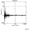
- FIG. 23 provides the same results but with a little bit more accuracy, because the IQ phase imbalance loop bandwidth has been reduced.
- K ampI 1.0e ⁇ 3
- K phase 1.0e ⁇ 3.
- FIG. 24 provides the final corrected QPSK constellation diagram, using the IQ envelope extraction algorithm for IQ estimation. This figure corresponds to FIG. 21 and FIG. 23 , respectively, and shows the results after all loops are in equilibrium.
- K ampI 1.0e ⁇ 3
- K phase 1.0e ⁇ 3.
- the present invention provides a mathematical way to extract from an OFDM envelope based signal the I-branch and Q-branch values.
- the algorithm has been proofed via a pre-equalization algorithm and an IQ phase imbalance adjustment algorithm.
- Both IQ adjustment algorithms in combination with the here presented IQ envelope extraction algorithm show a good stability and convergence. Because of the division operators some constraints with regards to the divisor have to be considered for a possible implementation. They depend on the signal amplitudes and will differ from implementation to implementation, but they are no principle restrictions to the algorithm.
- a frequency selective non-decision aided IQ phase imbalance adjustment and a frequency selective IQ amplitude adjustment are combined for direct conversion OFDM transmitters.
- analog filter miss matching is taken into account automatically because the LMS pre-equalizer works based on real coefficients and not based on a complex adaptive filter.
- the IQ symbol extraction from the envelope signal is solved by the IQ extraction algorithm.
Landscapes
- Engineering & Computer Science (AREA)
- Computer Networks & Wireless Communication (AREA)
- Signal Processing (AREA)
- Power Engineering (AREA)
- Digital Transmission Methods That Use Modulated Carrier Waves (AREA)
Abstract
Description
-
- Fully frequency selective adjustment loops on transmitter side are possible.
- A low cost direct conversion OFDM transceiver does not require a local transmitter receiver for IQ extraction.
- A low cost diode for the envelope measurement is possible.
S T,B(t)=I(t)+j·Q(t), (1)
where subscripts S and T denote transmitter and base band, respectively. The base band signal is delivered to the analog up-converter with the carrier frequency fc.
S T,f
S T,f
S T,f
S R,B,q(t)=[I(t)·cos(2πf C t)+Q(t)·sin(2πf C t+φ)]·e +j2πf
S R,B,q(t)=I(t)+Q(t)·sin(φ)+jQ(t)·cos(φ). (7)
S R,B,q(t)=I(t)+Q(t)·sin(φ)+jQ(t). (7a)
d(n)=d I(n)+j·d Q(n) (8)
y(n)=y I(n)+j·y Q(n) (9)
y(n)=√{square root over (y 2 I(n)+y 2 Q(n))}{square root over (y 2 I(n)+y 2 Q(n))} (10)
|A ananlog|(n)=√{square root over (y 2 I(n)+y 2 Q(n))}{square root over (y 2 I(n)+y 2 Q(n))}=|Adigital|(n)=√{square root over (d 2 I(n)+d2 Q(n))}{square root over (d 2 I(n)+d2 Q(n))} (11a)
|A analog|(n−1)=√{square root over (y 2 I(n−1)+y 2 Q(n−1))}{square root over (y 2 I(n−1)+y 2 Q(n−1))}=|A digital|(n−1)=√{square root over (d2 I(n−1)+d2 Q(n−1))}{square root over (d2 I(n−1)+d2 Q(n−1))} (11b)
A 2 analog(n)=y 2 I(n)+y 2 Q(n) (13b)
y 2 I(n)=A 2 analog(n)−y 2 Q(n) (14a)
y I(n)=√{square root over (y 2 I(n))}·signum(d I(n)) (15a)
y Q(n)=√{square root over (y 2 Q(n))}·signum(d Q(n)) (15b)
x[k]=d T [k]·w[k] (16)
y[k]=x T [k]·h[k] (17)
In the above equations (16) and (17), w[k] denotes the coefficient or weight vector of the pre-equalizer 133, and h[k] denotes the transfer vector of the
e[k]=d[k]−y[k]=d[k]−x T [k]·h[k] (18)
Inserting equation (16) to equation (18) results in the equation:
e[k]=d[k]−( D T [k]·w[k])T ·h[k] (19)
J{w[k]}=E<e 2 [k]>=E<(d[k]−y[k])2 >=E<(d[k]−w T [k]·D[k]·h[k])2> (20)
∇{E<e 2 [k]>}=−2·E<e[k]·x ˜ [k]> (21)
wherein x ˜[k] denotes a direction vector of the gradient, which corresponds to an assessment of the data matrix D[k] with the transfer vector h[k] of the
x ˜ [k]=D[k]·h[k]=h τ ·d[k−τ]=d[k−τ] (22)
wherein the data matrix D[k] represents a transformation matrix, which rotates the non-ideal transfer vector h[k] of the
∇{E # <e 2 [k]>}=−2·e[k]·d[k−τ] (22)
w[k+1]=w[k]+μ·e[k]·d[k−τ] (23)
E{I[n]·Q[n]}=0. (24)
E{(I[n]+Q[n]sin(φ) )·Q[n]}=
E{I[n]·Q[n]}+E{Q[n]sin(φ)·Q[n]}= (25)
E{Q 2 [n]sin(φ)}=
E{Q 2 [n]}sin(φ)=σQ 2·sin(φ)≈sin(φ)
e[n]=I[n]·Q[n]. (26)
The expectation value respectively the correction coefficient can then be provided by the integrator:
I′[n+1]−c[n]·Q[n+1]=I[n+1] (28)
e i [n]=Ĩ[n−(N−1)/2]·{tilde over (Q)}[n−(i−1)], i=1,2, . . . ,N (29)
where N is an odd number and the index of the error value is valid from 1 to N. N is selected on the basis of the analog filters. In practical cases in a WLAN environment, N typically has a value ranging from 7 to 19, but also other values may apply. The larger the value, the better the error value can be removed, at the cost of implementation difficulties.
e i[n]=Ĩ[n−(5−1)/2]·{tilde over (Q)}[n−(i−1)]=Ĩ[n−2]·{tilde over (Q)}[n−(i−1)].
e 1 [n]=Ĩ[n−2]·{tilde over (Q)}[n]
e 2 [n]=Ĩ[n−2]·{tilde over (Q)}[n−1]
e 3 [n]=Ĩ[n−2]·{tilde over (Q)}[n−2]
e 4 [n]=Ĩ[n−2]·{tilde over (Q)}[n−3]
e 5 [n]=Ĩ[n−2]·{tilde over (Q)}[n−4]
-
- Frequency selective IQ phase imbalance adjustment
- Frequency selective IQ amplitude imbalance adjustment
- Analog filter equalization respectively analog base-band filter miss-matching
Claims (27)
|A real(n)|=√{square root over (y I 2(n)+y Q 2(n))}{square root over (y I 2(n)+y Q 2(n))}=|A original(n)|=√{square root over (d I 2(n)+d Q 2(n))}{square root over (d I 2(n)+d Q 2(n))}
|A real(n−1)|=√{square root over (y I 2(n−1)+y Q 2(n−1))}{square root over (y I 2(n−1)+y Q 2(n−1))}=|A original(n−1)|=√{square root over (d I 2(n−1)+d Q 2(n−1))}{square root over (d I 2(n−1)+d Q 2(n−1))}
y I(n)=√{square root over (y 2 I(n))}·signum(d I(n))
y Q(n)=√{square root over (y 2 Q(n))}·signum(d Q(n))
|A real(n)|=√{square root over (y I 2(n)+y Q 2(n))}{square root over (y I 2(n)+y Q 2(n))}=|A original(n)|=√{square root over (d I 2(n)+d Q 2(n))}{square root over (d I 2(n)+d Q 2(n))}
|A real(n−1)|=√{square root over (y I 2(n31 1)+y Q 2(n31 1))}{square root over (y I 2(n31 1)+y Q 2(n31 1))}=|A original(n31 1)|=√{square root over (d I 2(n31 1)+d Q 2(n31 1))}{square root over (d I 2(n31 1)+d Q 2(n31 1))}
y I(n)=√{square root over (y 2 I(n))}·signum(d I(n))
y Q(n)=√{square root over (y 2 Q(n))}·signum(d Q(n))
Priority Applications (2)
| Application Number | Priority Date | Filing Date | Title |
|---|---|---|---|
| US10/408,106 US7627055B2 (en) | 2003-02-27 | 2003-04-08 | Error adjustment in direct conversion architectures |
| DE102004001998A DE102004001998A1 (en) | 2003-02-27 | 2004-01-14 | Error correction in direct implementation architectures |
Applications Claiming Priority (2)
| Application Number | Priority Date | Filing Date | Title |
|---|---|---|---|
| US44988003P | 2003-02-27 | 2003-02-27 | |
| US10/408,106 US7627055B2 (en) | 2003-02-27 | 2003-04-08 | Error adjustment in direct conversion architectures |
Publications (2)
| Publication Number | Publication Date |
|---|---|
| US20040193965A1 US20040193965A1 (en) | 2004-09-30 |
| US7627055B2 true US7627055B2 (en) | 2009-12-01 |
Family
ID=32853170
Family Applications (1)
| Application Number | Title | Priority Date | Filing Date |
|---|---|---|---|
| US10/408,106 Expired - Fee Related US7627055B2 (en) | 2003-02-27 | 2003-04-08 | Error adjustment in direct conversion architectures |
Country Status (2)
| Country | Link |
|---|---|
| US (1) | US7627055B2 (en) |
| DE (1) | DE102004001998A1 (en) |
Cited By (7)
| Publication number | Priority date | Publication date | Assignee | Title |
|---|---|---|---|---|
| US20080037684A1 (en) * | 2006-08-10 | 2008-02-14 | Ang-Sheng Lin | Communication system for utilizing single tone testing signal having specific frequency or combinations of dc value and single tone testing signal to calibrate impairments in transmitting signal |
| US20080130780A1 (en) * | 2006-11-30 | 2008-06-05 | Samsung Electro-Mechanics Co., Ltd. | Time-domain iq mismatch detection apparatus of ofdm receiver |
| US20120280749A1 (en) * | 2011-05-06 | 2012-11-08 | The Aerospace Corporation | Systems and methods for mitigating spectral regrowth from non-linear systems |
| US8798190B2 (en) | 2011-02-01 | 2014-08-05 | Blackberry Limited | Communications devices with envelope extraction and related methods |
| CN104065598A (en) * | 2013-03-21 | 2014-09-24 | 华为技术有限公司 | Method, apparatus and system for correcting broadband IQ disequilibrium |
| US9806877B2 (en) | 2015-12-08 | 2017-10-31 | Ali Corporation | Calibration method and calibration circuit |
| US10404380B2 (en) * | 2016-11-10 | 2019-09-03 | Fujitsu Limited | Compensation apparatus for offset drift, received signal recovery apparatus and receiver |
Families Citing this family (11)
| Publication number | Priority date | Publication date | Assignee | Title |
|---|---|---|---|---|
| EP1573995A1 (en) * | 2002-12-09 | 2005-09-14 | Philips Intellectual Property & Standards GmbH | Phase/gain imbalance estimation or compensation |
| EP1601129B1 (en) * | 2004-05-27 | 2008-09-03 | Synad Technologies Limited | Method of determining true error vector magnitude in a wireless lan |
| US7876856B2 (en) * | 2005-06-23 | 2011-01-25 | Texas Instrumentals Incorporated | Quadrature receiver with correction engine, coefficient controller and adaptation engine |
| CN101218744B (en) * | 2005-07-15 | 2010-05-26 | 日本电气株式会社 | Adaptive digital filter, FM receiver and signal processing method |
| WO2007110805A2 (en) * | 2006-03-28 | 2007-10-04 | Nxp B.V. | Transmitter with delay mismatch compensation |
| US7864882B2 (en) * | 2006-12-30 | 2011-01-04 | Motorola Mobility, Inc. | Method and apparatus for generating constant envelope modulation using a quadrature transmitter |
| US7801246B2 (en) * | 2006-12-30 | 2010-09-21 | Motorola Mobility, Inc. | Multi-mode communication device for generating constant envelope modulated signals using a quadrature modulator |
| US8233524B2 (en) * | 2009-03-12 | 2012-07-31 | Freescale Semiconductor, Inc. | Radio transmitter IQ imbalance measurement and correction methods and apparatus |
| US9385656B2 (en) * | 2011-11-10 | 2016-07-05 | Montage Technology (Shanghai) Co., Ltd. | Low complexity frequency selective IQ mismatch digital RX balancer and TX inverse balancer for non-ideal RF front-end |
| US8842771B2 (en) * | 2012-11-20 | 2014-09-23 | Tektronix, Inc. | Amplitude flatness and phase linearity calibration for RF sources |
| US10122568B2 (en) * | 2016-07-07 | 2018-11-06 | Microchip Technology Incorporated | Digital compensation of IQ coupling in communication receivers |
Citations (12)
| Publication number | Priority date | Publication date | Assignee | Title |
|---|---|---|---|---|
| US20010005402A1 (en) * | 1999-12-28 | 2001-06-28 | Fujitsu Limited | Distortion compensating apparatus |
| US6275685B1 (en) * | 1998-12-10 | 2001-08-14 | Nortel Networks Limited | Linear amplifier arrangement |
| US20020150171A1 (en) * | 2001-04-16 | 2002-10-17 | Myers Michael H. | Bandpass predistortion method and apparatus for radio transmission |
| US20030058959A1 (en) * | 2001-09-25 | 2003-03-27 | Caly Networks. | Combined digital adaptive pre-distorter and pre-equalizer system for modems in link hopping radio networks |
| US20030156658A1 (en) * | 2002-01-21 | 2003-08-21 | Evolium S.A.S. | Method and apparatus for preparing signals to be compared to establish predistortion at the input of an amplifier |
| US20030179831A1 (en) * | 2002-03-21 | 2003-09-25 | Deepnarayan Gupta | Power amplifier linearization |
| US20030179830A1 (en) * | 2002-03-25 | 2003-09-25 | Eidson Donald B. | Efficient, high fidelity transmission of modulation schemes through power-constrained remote relay stations by local transmit predistortion and local receiver feedback |
| US20030184374A1 (en) * | 2002-03-26 | 2003-10-02 | Xinping Huang | Type-based baseband predistorter function estimation technique for non-linear circuits |
| US6985704B2 (en) * | 2002-05-01 | 2006-01-10 | Dali Yang | System and method for digital memorized predistortion for wireless communication |
| US7085330B1 (en) * | 2002-02-15 | 2006-08-01 | Marvell International Ltd. | Method and apparatus for amplifier linearization using adaptive predistortion |
| US7170951B1 (en) * | 1999-06-18 | 2007-01-30 | Fraunhofer-Gesellschaft Zur Foerderung Der Angewandten Forschung E.V. | Device and method for predistorting a transmission signal to be transmitted via a nonlinear transmission path |
| US7382833B1 (en) * | 2001-08-16 | 2008-06-03 | Rockwell Collins, Inc. | System for phase, gain, and DC offset error correction for a quadrature modulator |
-
2003
- 2003-04-08 US US10/408,106 patent/US7627055B2/en not_active Expired - Fee Related
-
2004
- 2004-01-14 DE DE102004001998A patent/DE102004001998A1/en not_active Withdrawn
Patent Citations (12)
| Publication number | Priority date | Publication date | Assignee | Title |
|---|---|---|---|---|
| US6275685B1 (en) * | 1998-12-10 | 2001-08-14 | Nortel Networks Limited | Linear amplifier arrangement |
| US7170951B1 (en) * | 1999-06-18 | 2007-01-30 | Fraunhofer-Gesellschaft Zur Foerderung Der Angewandten Forschung E.V. | Device and method for predistorting a transmission signal to be transmitted via a nonlinear transmission path |
| US20010005402A1 (en) * | 1999-12-28 | 2001-06-28 | Fujitsu Limited | Distortion compensating apparatus |
| US20020150171A1 (en) * | 2001-04-16 | 2002-10-17 | Myers Michael H. | Bandpass predistortion method and apparatus for radio transmission |
| US7382833B1 (en) * | 2001-08-16 | 2008-06-03 | Rockwell Collins, Inc. | System for phase, gain, and DC offset error correction for a quadrature modulator |
| US20030058959A1 (en) * | 2001-09-25 | 2003-03-27 | Caly Networks. | Combined digital adaptive pre-distorter and pre-equalizer system for modems in link hopping radio networks |
| US20030156658A1 (en) * | 2002-01-21 | 2003-08-21 | Evolium S.A.S. | Method and apparatus for preparing signals to be compared to establish predistortion at the input of an amplifier |
| US7085330B1 (en) * | 2002-02-15 | 2006-08-01 | Marvell International Ltd. | Method and apparatus for amplifier linearization using adaptive predistortion |
| US20030179831A1 (en) * | 2002-03-21 | 2003-09-25 | Deepnarayan Gupta | Power amplifier linearization |
| US20030179830A1 (en) * | 2002-03-25 | 2003-09-25 | Eidson Donald B. | Efficient, high fidelity transmission of modulation schemes through power-constrained remote relay stations by local transmit predistortion and local receiver feedback |
| US20030184374A1 (en) * | 2002-03-26 | 2003-10-02 | Xinping Huang | Type-based baseband predistorter function estimation technique for non-linear circuits |
| US6985704B2 (en) * | 2002-05-01 | 2006-01-10 | Dali Yang | System and method for digital memorized predistortion for wireless communication |
Cited By (11)
| Publication number | Priority date | Publication date | Assignee | Title |
|---|---|---|---|---|
| US20080037684A1 (en) * | 2006-08-10 | 2008-02-14 | Ang-Sheng Lin | Communication system for utilizing single tone testing signal having specific frequency or combinations of dc value and single tone testing signal to calibrate impairments in transmitting signal |
| US7760817B2 (en) * | 2006-08-10 | 2010-07-20 | Mediatek Inc. | Communication system for utilizing single tone testing signal having specific frequency or combinations of DC value and single tone testing signal to calibrate impairments in transmitting signal |
| US20080130780A1 (en) * | 2006-11-30 | 2008-06-05 | Samsung Electro-Mechanics Co., Ltd. | Time-domain iq mismatch detection apparatus of ofdm receiver |
| US7903771B2 (en) * | 2006-11-30 | 2011-03-08 | Samsung Electro-Mechanics Co., Ltd. | Time-domain IQ mismatch detection apparatus of OFDM receiver |
| US8798190B2 (en) | 2011-02-01 | 2014-08-05 | Blackberry Limited | Communications devices with envelope extraction and related methods |
| US20120280749A1 (en) * | 2011-05-06 | 2012-11-08 | The Aerospace Corporation | Systems and methods for mitigating spectral regrowth from non-linear systems |
| US8711974B2 (en) * | 2011-05-06 | 2014-04-29 | The Aerospace Corporation | Systems and methods for mitigating spectral regrowth from non-linear systems |
| CN104065598A (en) * | 2013-03-21 | 2014-09-24 | 华为技术有限公司 | Method, apparatus and system for correcting broadband IQ disequilibrium |
| CN104065598B (en) * | 2013-03-21 | 2018-02-06 | 华为技术有限公司 | Broadband IQ disequilibrium regulatings method, apparatus and system |
| US9806877B2 (en) | 2015-12-08 | 2017-10-31 | Ali Corporation | Calibration method and calibration circuit |
| US10404380B2 (en) * | 2016-11-10 | 2019-09-03 | Fujitsu Limited | Compensation apparatus for offset drift, received signal recovery apparatus and receiver |
Also Published As
| Publication number | Publication date |
|---|---|
| DE102004001998A1 (en) | 2004-09-09 |
| US20040193965A1 (en) | 2004-09-30 |
Similar Documents
| Publication | Publication Date | Title |
|---|---|---|
| US7627055B2 (en) | Error adjustment in direct conversion architectures | |
| EP1523838B1 (en) | Adaptive pre-equalization method and apparatus | |
| JP4495159B2 (en) | Frequency domain equalizer for wireless communication system | |
| US10237095B2 (en) | Linear equalization for use in low latency high speed communication systems | |
| US8290458B2 (en) | System and method for IQ imbalance estimation using loopback with frequency offset | |
| US7453792B2 (en) | Receiver architecture for pilot based OFDM systems | |
| EP2194665B1 (en) | CFO and I/Q imbalance estimation and compensation | |
| US6560294B1 (en) | Phase estimation in carrier recovery of phase-modulated signals such as QAM signals | |
| US9537701B2 (en) | Joint estimation and compensation method of RF imperfections in LTE uplink system | |
| US20050201483A1 (en) | Error adjustment for multi-antenna transmitter | |
| US10284303B2 (en) | Feedforward decision-free pilot-aided phase noise estimation for coherent optical M-QAM systems | |
| US7620124B2 (en) | Direct conversion receiver and receiving method | |
| US20100239033A1 (en) | Joint carrier synchronization and channel equalization method for OFDM systems | |
| WO2014194940A1 (en) | Coherent optical receiver | |
| JP2002526948A (en) | Echo phase offset correction in multicarrier demodulation systems | |
| US20050041754A1 (en) | Method and appatatus for I/Q mismatch calibration of transmitter | |
| TWI603603B (en) | In the downlink transmission system to solve the imperfect joint estimation of pre-compensation method | |
| EP2135412A2 (en) | Channel estimation using frequency smoothing | |
| JPH06500914A (en) | Apparatus and method for adjusting signal points, equalizer gains, etc. | |
| EP1130866B1 (en) | Correction of quadrature and gain errors in homodyne receivers | |
| KR100744092B1 (en) | Direct conversion receiver and reception method | |
| EP1665710B1 (en) | Apparatus and method for adaptive orthogonality correction |
Legal Events
| Date | Code | Title | Description |
|---|---|---|---|
| AS | Assignment |
Owner name: NOKIA CORPORATION, FINLAND Free format text: ASSIGNMENT OF ASSIGNORS INTEREST;ASSIGNOR:COERSMEIER, EDMUND;REEL/FRAME:014341/0279 Effective date: 20030612 |
|
| FEPP | Fee payment procedure |
Free format text: PAYOR NUMBER ASSIGNED (ORIGINAL EVENT CODE: ASPN); ENTITY STATUS OF PATENT OWNER: LARGE ENTITY |
|
| REMI | Maintenance fee reminder mailed | ||
| LAPS | Lapse for failure to pay maintenance fees | ||
| STCH | Information on status: patent discontinuation |
Free format text: PATENT EXPIRED DUE TO NONPAYMENT OF MAINTENANCE FEES UNDER 37 CFR 1.362 |
|
| STCH | Information on status: patent discontinuation |
Free format text: PATENT EXPIRED DUE TO NONPAYMENT OF MAINTENANCE FEES UNDER 37 CFR 1.362 |
|
| FP | Lapsed due to failure to pay maintenance fee |
Effective date: 20131201 |