US7617424B2 - Error monitoring for serial links - Google Patents

Error monitoring for serial links Download PDF

Info

Publication number
US7617424B2
US7617424B2 US11/323,111 US32311105A US7617424B2 US 7617424 B2 US7617424 B2 US 7617424B2 US 32311105 A US32311105 A US 32311105A US 7617424 B2 US7617424 B2 US 7617424B2
Authority
US
United States
Prior art keywords
bit
coupled
bit counters
counter
multiplexer
Prior art date
Legal status (The legal status is an assumption and is not a legal conclusion. Google has not performed a legal analysis and makes no representation as to the accuracy of the status listed.)
Expired - Fee Related, expires
Application number
US11/323,111
Other versions
US20070157054A1 (en
Inventor
Timothy Frodsham
Zale T. Schoenborn
Sanjay Dabral
Muraleendhara Navada
Current Assignee (The listed assignees may be inaccurate. Google has not performed a legal analysis and makes no representation or warranty as to the accuracy of the list.)
Intel Corp
Original Assignee
Intel Corp
Priority date (The priority date is an assumption and is not a legal conclusion. Google has not performed a legal analysis and makes no representation as to the accuracy of the date listed.)
Filing date
Publication date
Application filed by Intel Corp filed Critical Intel Corp
Priority to US11/323,111 priority Critical patent/US7617424B2/en
Publication of US20070157054A1 publication Critical patent/US20070157054A1/en
Assigned to INTEL CORPORATION reassignment INTEL CORPORATION ASSIGNMENT OF ASSIGNORS INTEREST (SEE DOCUMENT FOR DETAILS). Assignors: SCHOENBORN, ZALE T., DABRAL, SANJAY, NAVADA, MURALEENDHARA, FRODSHAM, TIMOTHY
Priority to US12/115,360 priority patent/US8195996B2/en
Application granted granted Critical
Publication of US7617424B2 publication Critical patent/US7617424B2/en
Expired - Fee Related legal-status Critical Current
Adjusted expiration legal-status Critical

Links

Images

Classifications

    • HELECTRICITY
    • H04ELECTRIC COMMUNICATION TECHNIQUE
    • H04LTRANSMISSION OF DIGITAL INFORMATION, e.g. TELEGRAPHIC COMMUNICATION
    • H04L1/00Arrangements for detecting or preventing errors in the information received
    • H04L1/24Testing correct operation
    • H04L1/242Testing correct operation by comparing a transmitted test signal with a locally generated replica

Definitions

  • Embodiments of the invention relate to a physical layer interface of a computing system. More particularly, embodiments of the invention relate to error monitoring for serial links between components of a computing system.
  • Some physical link specifications incorporate self-test hooks that can be used to collect, for example, eye diagrams, equivalent time oscilloscope traces and/or bit error rate diagrams.
  • self-test hooks may be sufficiently inflexible, which may result in a complex and/or time consuming testing and debugging process.
  • FIG. 1 is a block diagram of one embodiment of an apparatus for a physical interconnect.
  • FIG. 2 is a conceptual illustration of one embodiment of a system that may utilize point-to-point interconnects.
  • FIG. 3 is a block diagram of one embodiment of a flexible error counting architecture.
  • FIG. 4 a is a conceptual illustration of error checking using a single register for each bit of an incoming data stream.
  • FIG. 4 b is a conceptual illustration of error checking using two registers for alternating bits of an incoming data stream to be stored in respective registers.
  • FIG. 5 is a conceptual illustration of error checking using multiple registers for selected bits of an incoming data stream to be stored in respective registers.
  • FIG. 6 is a block diagram of one embodiment of circuitry for error checking using selected bits from incoming data streams.
  • pattern generation and comparison may be utilized for error checking purposes.
  • flexibility in the error checking functionality may be provided to enable targeted, hardware specific testing and generic tools such as an “on-die oscilloscope.”
  • Programmable offsets and intervals in the error checking mechanism may allow support of targeted tests and on-die oscilloscope functionality.
  • measurements may be taken over a range of frequencies, timing and/or voltage stress factors.
  • large counters may be required to measure the expected error rate.
  • smaller counters may be used because the error rate may be lower.
  • simply utilizing large counters to support a full range of testing may be relatively expensive in terms of circuit size and/or power consumption.
  • individual counters may be used for individual data lanes. Multiple individual counters may be multiplexed to provide an extended counter for a selected data lane. This extended error counting functionality may allow flexibility to characterize high bit error rates for a selected data lane.
  • FIG. 1 is a block diagram of one embodiment of an apparatus for a physical interconnect.
  • the apparatus depicts a physical layer for a cache-coherent, link-based interconnect scheme for a processor, chipset, and/or I/O bridge components.
  • the physical interconnect may be performed by each physical layer of an integrated device.
  • the physical interconnect may support training and testing in association with use of an oscilloscope probe or other test equipment to monitor the physical interconnect.
  • the physical layer may provide communication between two ports over a physical interconnect comprising two uni-directional links.
  • one unidirectional link 104 from a first transmit port 150 of a first integrated device to a first receiver port 150 of a second integrated device.
  • a second uni-directional link 106 from a first transmit port 150 of the second integrated device to a first receiver port 150 of the first integrated device.
  • the claimed subject matter is not limited to two uni-directional links.
  • FIG. 2 is a conceptual illustration of one embodiment of a system that may utilize point-to-point interconnects.
  • the system of FIG. 2 may utilize a point-to-point architecture that supports a layered protocol scheme.
  • the system may include a plurality of caching agents and home agents coupled to a network fabric.
  • the network fabric may adhere to a layered protocol scheme and comprised of: a physical layer, a link layer, a routing layer, a transport layer and a protocol layer (as depicted in connection with FIG. 1 ).
  • the fabric may facilitate transporting messages from one protocol (home or caching agent) to another protocol for a point-to-point network.
  • FIG. 2 is a high level, simplified abstraction of a protocol architecture that may utilize one or more point-to-point links.
  • the fabric may facilitate transporting messages from one protocol (caching processor or caching aware memory controller) to another protocol for a point-to-point network.
  • Each caching-aware memory controller may be coupled with memory that may include, for example, dynamic random access memory (DRAM), flash memory, or any other type of memory known in the art.
  • DRAM dynamic random access memory
  • flash memory any other type of memory known in the art.
  • FIG. 3 is a block diagram of one embodiment of a flexible error counting architecture.
  • each data lane corresponds to a serial physical link; however, any data communications medium may be utilized.
  • the configuration of FIG. 3 may be used, for example, to count bit errors that occur during transmission of data over a physical link.
  • each data line may be coupled with a N-bit counter (e.g., 310 , 312 , 318 ).
  • a N-bit counter e.g., 310 , 312 , 318 .
  • Any size counter may be used, for example, each counter may be an 8-bit counter.
  • the size of the counter used may be selected based on, for example, the expected error rate for a relatively low end of a frequency, timing and/or voltage stress factors to be used in testing.
  • the N-bit counters may be any size (e.g., 8-bit, 12-bit, 4-bit, 24-bit, 32-bit).
  • Each of the N-bit counters may be coupled with multiplexor 330 .
  • Control signals may be provided to multiplexor 330 by any type of control circuitry.
  • the control signals may be provided by software controlled circuitry that allows a user to determine the configuration of the counters and multiplexor.
  • the control signals may be provided by firmware to implement a pre-programmed testing sequence.
  • Extended counter 350 may be any size counter (e.g., 24-bit, 32-bit, 16-bit, 8-bit, 56-bit). For example, if N-bit counters 310 , 312 , . . . 318 are 8-bit counters and extended counter 350 is a 24-bit counter, a selected data lane may have 32 bits of error counting. Thus, a single extended counter may be shared between multiple smaller counters to provide a greater error counting capacity than the N-bit counters alone.
  • the error count provided by the combination of the selected N-bit counter and extended counter 350 may be accessible through a debug or testability register. In one embodiment, the following register configuration may be used.
  • a set of testability registers may be used to support targeted tests and/or on-die oscilloscope functionality.
  • a register may be utilized to store each bit of an incoming data stream. This is conceptually illustrated in FIG. 4 a . While FIGS. 4 a , 4 b and 5 provide examples of 128 bits, any number of bits my be used.
  • FIG. 4 b is a conceptual illustration of error checking using two registers for alternating bits of an incoming data stream to be stored in respective registers.
  • error checking circuitry may have multiple fields that may be used to selectively program sample and store incoming data bits to various testability registers. By interleaving bits one receiver may sample, for example, the odd bits while a second receiver may sample the even bits.
  • a testing instruction and/or a testing register may include fields that correspond to a start of testing and an offset, or interval, that may indicate the sampling interval.
  • the first receiver that samples the odd bits may have an offset of “0” and an interval of “2” to indicate that the first bit and every second subsequent bit should be sampled.
  • the second receiver that samples the even bits may have an offset of “1” and an interval of “2” to indicate that the second bit and every second subsequent bit should be sampled.
  • Other offsets and intervals may be used to provide different testing scenarios.
  • an initial round of testing may be accomplished using a first set of offsets and intervals. This could be, for example, every fourth or every tenth bit.
  • the sampled data may be compared to expected data to determine whether the data appears to be as expected. If so, the test results may be considered satisfactory. If, however, one or more of the bits are not as expected, a different offset and/or interval may be used to provide additional testing information that may be used to debug the underlying system or configuration.
  • FIG. 5 is a conceptual illustration of error checking using multiple registers for selected bits of an incoming data stream to be stored in respective registers.
  • each individual bit in a stream of data may be characterized to build an on-die oscilloscope trace.
  • the example of FIG. 5 illustrates a first receiver with offset of “0” and an interval of “128,” a second receiver with an offset of “1” and an interval of “128” and so on.
  • the greater the interval the less inter-symbol interference (ISI) experienced.
  • ISI inter-symbol interference
  • the individual bits that are captured using the offset and interval parameters may be combined to generate an on-die oscilloscope trace using suitable techniques known in the art.
  • the techniques and architectures described herein may provide improved raw data from which to generate testing data. Another advantage of the techniques described herein is that, using the offset and interval parameters, the testing process may be more efficient because the granularity of the testing data may be tailored to the specific situation.
  • FIG. 6 is a block diagram of one embodiment of circuitry for error checking using selected bits from incoming data streams.
  • Multiple receiver circuits e.g., 610 , 612 , 618
  • the receivers may be coupled with control circuitry 630 , which may cause the receivers to selectively sample data according to offset and interval parameters for the respective receivers, as described above.
  • Control circuitry 630 may be coupled to receive the parameters from an external source, for example, one or more debug or testing registers, a software application, etc.
  • Comparison circuitry 650 may be coupled with control circuitry 630 to compare the sampled data values to expected data values.
  • the sampled data values may be stored, for example, in registers in the respective receivers and/or in registers in control circuitry 630 .
  • the sampled data values may be accessed in any manner known in the art.

Landscapes

  • Engineering & Computer Science (AREA)
  • Computer Networks & Wireless Communication (AREA)
  • Signal Processing (AREA)
  • Detection And Prevention Of Errors In Transmission (AREA)

Abstract

Methods, apparatuses and systems for physical link error data capture and analysis.

Description

TECHNICAL FIELD
Embodiments of the invention relate to a physical layer interface of a computing system. More particularly, embodiments of the invention relate to error monitoring for serial links between components of a computing system.
BACKGROUND
In computing systems, as operating frequencies increase external testing of physical links becomes increasingly difficult. Some physical link specifications incorporate self-test hooks that can be used to collect, for example, eye diagrams, equivalent time oscilloscope traces and/or bit error rate diagrams. However, these self-test hooks may be sufficiently inflexible, which may result in a complex and/or time consuming testing and debugging process.
BRIEF DESCRIPTION OF THE DRAWINGS
Embodiments of the invention are illustrated by way of example, and not by way of limitation, in the figures of the accompanying drawings in which like reference numerals refer to similar elements.
FIG. 1 is a block diagram of one embodiment of an apparatus for a physical interconnect.
FIG. 2 is a conceptual illustration of one embodiment of a system that may utilize point-to-point interconnects.
FIG. 3 is a block diagram of one embodiment of a flexible error counting architecture.
FIG. 4 a is a conceptual illustration of error checking using a single register for each bit of an incoming data stream.
FIG. 4 b is a conceptual illustration of error checking using two registers for alternating bits of an incoming data stream to be stored in respective registers.
FIG. 5 is a conceptual illustration of error checking using multiple registers for selected bits of an incoming data stream to be stored in respective registers.
FIG. 6 is a block diagram of one embodiment of circuitry for error checking using selected bits from incoming data streams.
DETAILED DESCRIPTION
In the following description, numerous specific details are set forth. However, embodiments of the invention may be practiced without these specific details. In other instances, well-known circuits, structures and techniques have not been shown in detail in order not to obscure the understanding of this description.
In one embodiment, pattern generation and comparison may be utilized for error checking purposes. As described in greater detail below, flexibility in the error checking functionality may be provided to enable targeted, hardware specific testing and generic tools such as an “on-die oscilloscope.” Programmable offsets and intervals in the error checking mechanism may allow support of targeted tests and on-die oscilloscope functionality.
In order to adequately characterize error rates on a high-speed serial link, measurements may be taken over a range of frequencies, timing and/or voltage stress factors. At the high end of frequency and stress, large counters may be required to measure the expected error rate. At the low end of frequency and stress, smaller counters may be used because the error rate may be lower. However, simply utilizing large counters to support a full range of testing may be relatively expensive in terms of circuit size and/or power consumption.
As described in greater detail below, in one embodiment, individual counters may be used for individual data lanes. Multiple individual counters may be multiplexed to provide an extended counter for a selected data lane. This extended error counting functionality may allow flexibility to characterize high bit error rates for a selected data lane.
FIG. 1 is a block diagram of one embodiment of an apparatus for a physical interconnect. In one aspect, the apparatus depicts a physical layer for a cache-coherent, link-based interconnect scheme for a processor, chipset, and/or I/O bridge components. For example, the physical interconnect may be performed by each physical layer of an integrated device. The physical interconnect may support training and testing in association with use of an oscilloscope probe or other test equipment to monitor the physical interconnect.
Specifically, the physical layer may provide communication between two ports over a physical interconnect comprising two uni-directional links. Specifically, one unidirectional link 104 from a first transmit port 150 of a first integrated device to a first receiver port 150 of a second integrated device. Likewise, a second uni-directional link 106 from a first transmit port 150 of the second integrated device to a first receiver port 150 of the first integrated device. However, the claimed subject matter is not limited to two uni-directional links.
FIG. 2 is a conceptual illustration of one embodiment of a system that may utilize point-to-point interconnects. In one embodiment, the system of FIG. 2 may utilize a point-to-point architecture that supports a layered protocol scheme. In one embodiment, the system may include a plurality of caching agents and home agents coupled to a network fabric. For example, the network fabric may adhere to a layered protocol scheme and comprised of: a physical layer, a link layer, a routing layer, a transport layer and a protocol layer (as depicted in connection with FIG. 1). The fabric may facilitate transporting messages from one protocol (home or caching agent) to another protocol for a point-to-point network.
FIG. 2 is a high level, simplified abstraction of a protocol architecture that may utilize one or more point-to-point links. The fabric may facilitate transporting messages from one protocol (caching processor or caching aware memory controller) to another protocol for a point-to-point network. Each caching-aware memory controller may be coupled with memory that may include, for example, dynamic random access memory (DRAM), flash memory, or any other type of memory known in the art.
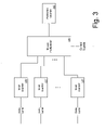
FIG. 3 is a block diagram of one embodiment of a flexible error counting architecture. In one embodiment, each data lane corresponds to a serial physical link; however, any data communications medium may be utilized. The configuration of FIG. 3 may be used, for example, to count bit errors that occur during transmission of data over a physical link.
In one embodiment, each data line may be coupled with a N-bit counter (e.g., 310, 312, 318). Any size counter may be used, for example, each counter may be an 8-bit counter. The size of the counter used may be selected based on, for example, the expected error rate for a relatively low end of a frequency, timing and/or voltage stress factors to be used in testing. The N-bit counters may be any size (e.g., 8-bit, 12-bit, 4-bit, 24-bit, 32-bit). Each of the N-bit counters may be coupled with multiplexor 330.
Control signals may be provided to multiplexor 330 by any type of control circuitry. For example, the control signals may be provided by software controlled circuitry that allows a user to determine the configuration of the counters and multiplexor. In another embodiment, the control signals may be provided by firmware to implement a pre-programmed testing sequence.
The output of multiplexor 330 may be coupled with extended counter 350. Extended counter 350 may be any size counter (e.g., 24-bit, 32-bit, 16-bit, 8-bit, 56-bit). For example, if N- bit counters 310, 312, . . . 318 are 8-bit counters and extended counter 350 is a 24-bit counter, a selected data lane may have 32 bits of error counting. Thus, a single extended counter may be shared between multiple smaller counters to provide a greater error counting capacity than the N-bit counters alone.
In one embodiment, the error count provided by the combination of the selected N-bit counter and extended counter 350 may be accessible through a debug or testability register. In one embodiment, the following register configuration may be used.
TABLE 1
Register configuration.
Default
Bits Width Name Value Value/Description
31 1 Error 0 If set, indicates that the error
Overflow counter has been extended
to extended counter. Bit cleared
upon Loopback.
30:0 31 Lane Error 0 Lane Error Counter is the
Counter accumulation of errors in a
selected lane. Exact number of bits
in counter may vary by
architecture implementation.
Counter cleared upon Loopback.

The register configuration of Table 1 corresponds to a total counter (N-bit counter plus extended counter) width of 32 bits. In alternate embodiments, other register configurations may be supported. The register may be accessed in any manner known in the art and the value stored in the register may be used in any manner known in the art.
In one embodiment, a set of testability registers may be used to support targeted tests and/or on-die oscilloscope functionality. In one embodiment, a register may be utilized to store each bit of an incoming data stream. This is conceptually illustrated in FIG. 4 a. While FIGS. 4 a, 4 b and 5 provide examples of 128 bits, any number of bits my be used.
FIG. 4 b is a conceptual illustration of error checking using two registers for alternating bits of an incoming data stream to be stored in respective registers. In one embodiment, error checking circuitry may have multiple fields that may be used to selectively program sample and store incoming data bits to various testability registers. By interleaving bits one receiver may sample, for example, the odd bits while a second receiver may sample the even bits.
In one embodiment, a testing instruction and/or a testing register may include fields that correspond to a start of testing and an offset, or interval, that may indicate the sampling interval. In the example of FIG. 4 b, the first receiver that samples the odd bits may have an offset of “0” and an interval of “2” to indicate that the first bit and every second subsequent bit should be sampled. The second receiver that samples the even bits may have an offset of “1” and an interval of “2” to indicate that the second bit and every second subsequent bit should be sampled. Other offsets and intervals may be used to provide different testing scenarios.
For example, an initial round of testing may be accomplished using a first set of offsets and intervals. This could be, for example, every fourth or every tenth bit. The sampled data may be compared to expected data to determine whether the data appears to be as expected. If so, the test results may be considered satisfactory. If, however, one or more of the bits are not as expected, a different offset and/or interval may be used to provide additional testing information that may be used to debug the underlying system or configuration.
FIG. 5 is a conceptual illustration of error checking using multiple registers for selected bits of an incoming data stream to be stored in respective registers. In one embodiment, each individual bit in a stream of data may be characterized to build an on-die oscilloscope trace. The example of FIG. 5 illustrates a first receiver with offset of “0” and an interval of “128,” a second receiver with an offset of “1” and an interval of “128” and so on. In general, the greater the interval the less inter-symbol interference (ISI) experienced.
The individual bits that are captured using the offset and interval parameters may be combined to generate an on-die oscilloscope trace using suitable techniques known in the art. The techniques and architectures described herein may provide improved raw data from which to generate testing data. Another advantage of the techniques described herein is that, using the offset and interval parameters, the testing process may be more efficient because the granularity of the testing data may be tailored to the specific situation.
FIG. 6 is a block diagram of one embodiment of circuitry for error checking using selected bits from incoming data streams. Multiple receiver circuits (e.g., 610, 612, 618) may be coupled to receive data via a data lane. The receivers may be coupled with control circuitry 630, which may cause the receivers to selectively sample data according to offset and interval parameters for the respective receivers, as described above. Control circuitry 630 may be coupled to receive the parameters from an external source, for example, one or more debug or testing registers, a software application, etc.
Comparison circuitry 650 may be coupled with control circuitry 630 to compare the sampled data values to expected data values. The sampled data values may be stored, for example, in registers in the respective receivers and/or in registers in control circuitry 630. The sampled data values may be accessed in any manner known in the art.
Reference in the specification to “one embodiment” or “an embodiment” means that a particular feature, structure, or characteristic described in connection with the embodiment is included in at least one embodiment of the invention. The appearances of the phrase “in one embodiment” in various places in the specification are not necessarily all referring to the same embodiment.
While the invention has been described in terms of several embodiments, those skilled in the art will recognize that the invention is not limited to the embodiments described, but can be practiced with modification and alteration within the spirit and scope of the appended claims. The description is thus to be regarded as illustrative instead of limiting.

Claims (10)

1. An apparatus comprising:
a plurality of N-bit counters each coupled with a plurality of receivers coupled with corresponding serial data links;
a multiplexer coupled with the plurality of N-bit counters to select an output signal from one of the plurality of N-bit counters; and
an expanded counter coupled with the output of the multiplexer to count output signals from the multiplexer.
2. The apparatus of claim 1 wherein the N-bit counters comprise 8-bit counters.
3. The apparatus of claim 1 wherein the N-bit counters are coupled to count errors detected on the respective serial links.
4. The apparatus of claim 1 further comprising a register coupled to store a value based, at least in part, on a selected N-bit counter and the expanded counter.
5. A system comprising:
a plurality of test registers;
a port to communicate via a point-to-point serial link having a receiver and a control circuit coupled with the receiver, the control circuit having a plurality of N-bit counters each coupled with a serial data link, a multiplexer coupled with the plurality of N-bit counters to select an output signal from one of the plurality of N-bit counters, and an expanded counter coupled with the output of the multiplexer to count output signals from the multiplexer, the control circuit coupled with the plurality of test registers.
6. The system of claim 5 wherein the N-bit counters comprise 8-bit counters.
7. The system of claim 5 wherein the N-bit counters are coupled to count errors detected on the respective serial links.
8. The system of claim 5 further comprising a register coupled to store a value based, at least in part, on a selected N-bit counter and the expanded counter.
9. A method comprising:
counting bit errors detected in a plurality of data streams received via a plurality of point-to-point serial links using a plurality of corresponding N-bit counters; and
selectively enabling a multiplexer to pass output signals from the plurality of N-bit counters to an expanded counter to expand counting capacity utilizing the extended counter to enable bit error counting beyond a capacity of the N-bit counters.
10. The method of claim 9 wherein at least one of the N-bit counters comprise 8-bit counters.
US11/323,111 2005-12-30 2005-12-30 Error monitoring for serial links Expired - Fee Related US7617424B2 (en)

Priority Applications (2)

Application Number Priority Date Filing Date Title
US11/323,111 US7617424B2 (en) 2005-12-30 2005-12-30 Error monitoring for serial links
US12/115,360 US8195996B2 (en) 2005-12-30 2008-05-05 Apparatuses, systems and methods for detecting errors in data streams on point-to-point serial links

Applications Claiming Priority (1)

Application Number Priority Date Filing Date Title
US11/323,111 US7617424B2 (en) 2005-12-30 2005-12-30 Error monitoring for serial links

Related Child Applications (1)

Application Number Title Priority Date Filing Date
US12/115,360 Division US8195996B2 (en) 2005-12-30 2008-05-05 Apparatuses, systems and methods for detecting errors in data streams on point-to-point serial links

Publications (2)

Publication Number Publication Date
US20070157054A1 US20070157054A1 (en) 2007-07-05
US7617424B2 true US7617424B2 (en) 2009-11-10

Family

ID=38226076

Family Applications (2)

Application Number Title Priority Date Filing Date
US11/323,111 Expired - Fee Related US7617424B2 (en) 2005-12-30 2005-12-30 Error monitoring for serial links
US12/115,360 Expired - Fee Related US8195996B2 (en) 2005-12-30 2008-05-05 Apparatuses, systems and methods for detecting errors in data streams on point-to-point serial links

Family Applications After (1)

Application Number Title Priority Date Filing Date
US12/115,360 Expired - Fee Related US8195996B2 (en) 2005-12-30 2008-05-05 Apparatuses, systems and methods for detecting errors in data streams on point-to-point serial links

Country Status (1)

Country Link
US (2) US7617424B2 (en)

Cited By (5)

* Cited by examiner, † Cited by third party
Publication number Priority date Publication date Assignee Title
US20090138767A1 (en) * 2007-11-27 2009-05-28 Nec Electronics Corporation Self-diagnostic circuit and self-diagnostic method for detecting errors
US8627156B1 (en) * 2010-10-26 2014-01-07 Agilent Technologies, Inc. Method and system of testing bit error rate using signal with mixture of scrambled and unscrambled bits
US9076499B2 (en) 2012-12-28 2015-07-07 Intel Corporation Refresh rate performance based on in-system weak bit detection
US9196384B2 (en) 2012-12-28 2015-11-24 Intel Corporation Memory subsystem performance based on in-system weak bit detection
US9536626B2 (en) 2013-02-08 2017-01-03 Intel Corporation Memory subsystem I/O performance based on in-system empirical testing

Families Citing this family (10)

* Cited by examiner, † Cited by third party
Publication number Priority date Publication date Assignee Title
US7836352B2 (en) * 2006-06-30 2010-11-16 Intel Corporation Method and apparatus for improving high availability in a PCI express link through predictive failure analysis
WO2010071628A1 (en) * 2008-12-15 2010-06-24 Hewlett-Packard Development Company, L.P. Detecting an unreliable link in a computer system
US8862944B2 (en) * 2010-06-24 2014-10-14 International Business Machines Corporation Isolation of faulty links in a transmission medium
CN102760086B (en) * 2012-07-06 2016-06-08 北京泛华恒兴科技有限公司 Data detection control method and device based on flexible test technology
US9003246B2 (en) 2012-09-29 2015-04-07 Intel Corporation Functional memory array testing with a transaction-level test engine
US8996934B2 (en) 2012-09-29 2015-03-31 Intel Corporation Transaction-level testing of memory I/O and memory device
US9009540B2 (en) 2012-12-05 2015-04-14 Intel Corporation Memory subsystem command bus stress testing
US9009531B2 (en) 2012-12-05 2015-04-14 Intel Corporation Memory subsystem data bus stress testing
US9692402B2 (en) 2014-12-25 2017-06-27 Intel Corporation Method, apparatus, system for centering in a high performance interconnect
WO2019215871A1 (en) * 2018-05-10 2019-11-14 三菱電機株式会社 Electronic control apparatus

Citations (12)

* Cited by examiner, † Cited by third party
Publication number Priority date Publication date Assignee Title
US5036515A (en) * 1989-05-30 1991-07-30 Motorola, Inc. Bit error rate detection
US5142651A (en) * 1991-10-09 1992-08-25 United States Of America As Represented By The Secretary Of The Navy Uninterrupted, enhanced-rate, event-time recorder with mixed-speed counter modules
US5146324A (en) * 1990-07-31 1992-09-08 Ampex Corporation Data compression using a feedforward quantization estimator
US5301219A (en) * 1991-12-18 1994-04-05 The United States Of America As Represented By The Secretary Of The Navy Uninterrupted, enhanced-rate event sequencer with mixed-speed counter modules
US5317706A (en) * 1989-11-15 1994-05-31 Ncr Corporation Memory expansion method and apparatus in a virtual memory system
US5497406A (en) * 1993-09-29 1996-03-05 Sgs-Thomson Microelectronics S.A. Multi-standard generator of periodic signals
US6973602B1 (en) * 2002-09-05 2005-12-06 Ciena Corporation Link and path-level error performance monitoring
US7032139B1 (en) * 2002-03-18 2006-04-18 Finisar Corporation Bit error rate tester
US7062687B1 (en) * 1999-07-12 2006-06-13 International Business Machines Corporation Apparatus and method for setting a data rate in a wireless communication system
US7231558B2 (en) * 2002-03-18 2007-06-12 Finisar Corporation System and method for network error rate testing
US7246274B2 (en) * 2004-09-10 2007-07-17 Rambus Inc. Method and apparatus for estimating random jitter (RJ) and deterministic jitter (DJ) from bit error rate (BER)
US7386767B1 (en) * 2004-10-05 2008-06-10 Altera Corporation Programmable bit error rate monitor for serial interface

Family Cites Families (4)

* Cited by examiner, † Cited by third party
Publication number Priority date Publication date Assignee Title
US6988227B1 (en) * 2001-06-25 2006-01-17 Silicon Laboratories Inc. Method and apparatus for bit error rate detection
US7571360B1 (en) * 2004-10-26 2009-08-04 National Semiconductor Corporation System and method for providing a clock and data recovery circuit with a fast bit error rate self test capability
US7668274B2 (en) * 2005-04-06 2010-02-23 Freescale Semiconductor, Inc. Eye center retraining system and method
JP2009129301A (en) * 2007-11-27 2009-06-11 Nec Electronics Corp Self-diagnostic circuit and self-diagnostic method

Patent Citations (13)

* Cited by examiner, † Cited by third party
Publication number Priority date Publication date Assignee Title
US5036515A (en) * 1989-05-30 1991-07-30 Motorola, Inc. Bit error rate detection
US5317706A (en) * 1989-11-15 1994-05-31 Ncr Corporation Memory expansion method and apparatus in a virtual memory system
US5146324A (en) * 1990-07-31 1992-09-08 Ampex Corporation Data compression using a feedforward quantization estimator
US5142651A (en) * 1991-10-09 1992-08-25 United States Of America As Represented By The Secretary Of The Navy Uninterrupted, enhanced-rate, event-time recorder with mixed-speed counter modules
US5301219A (en) * 1991-12-18 1994-04-05 The United States Of America As Represented By The Secretary Of The Navy Uninterrupted, enhanced-rate event sequencer with mixed-speed counter modules
US5581163A (en) * 1993-09-29 1996-12-03 Sgs-Thomson Microelectronics S.A. Generator of periodic signals
US5497406A (en) * 1993-09-29 1996-03-05 Sgs-Thomson Microelectronics S.A. Multi-standard generator of periodic signals
US7062687B1 (en) * 1999-07-12 2006-06-13 International Business Machines Corporation Apparatus and method for setting a data rate in a wireless communication system
US7032139B1 (en) * 2002-03-18 2006-04-18 Finisar Corporation Bit error rate tester
US7231558B2 (en) * 2002-03-18 2007-06-12 Finisar Corporation System and method for network error rate testing
US6973602B1 (en) * 2002-09-05 2005-12-06 Ciena Corporation Link and path-level error performance monitoring
US7246274B2 (en) * 2004-09-10 2007-07-17 Rambus Inc. Method and apparatus for estimating random jitter (RJ) and deterministic jitter (DJ) from bit error rate (BER)
US7386767B1 (en) * 2004-10-05 2008-06-10 Altera Corporation Programmable bit error rate monitor for serial interface

Cited By (7)

* Cited by examiner, † Cited by third party
Publication number Priority date Publication date Assignee Title
US20090138767A1 (en) * 2007-11-27 2009-05-28 Nec Electronics Corporation Self-diagnostic circuit and self-diagnostic method for detecting errors
US7904771B2 (en) * 2007-11-27 2011-03-08 Renesas Electronics Corporation Self-diagnostic circuit and self-diagnostic method for detecting errors
US8627156B1 (en) * 2010-10-26 2014-01-07 Agilent Technologies, Inc. Method and system of testing bit error rate using signal with mixture of scrambled and unscrambled bits
US9076499B2 (en) 2012-12-28 2015-07-07 Intel Corporation Refresh rate performance based on in-system weak bit detection
US9196384B2 (en) 2012-12-28 2015-11-24 Intel Corporation Memory subsystem performance based on in-system weak bit detection
US9536626B2 (en) 2013-02-08 2017-01-03 Intel Corporation Memory subsystem I/O performance based on in-system empirical testing
US10446222B2 (en) 2013-02-08 2019-10-15 Intel Corporation Memory subsystem I/O performance based on in-system empirical testing

Also Published As

Publication number Publication date
US8195996B2 (en) 2012-06-05
US20080209306A1 (en) 2008-08-28
US20070157054A1 (en) 2007-07-05

Similar Documents

Publication Publication Date Title
US7617424B2 (en) Error monitoring for serial links
US7464307B2 (en) High performance serial bus testing methodology
JP5576880B2 (en) Interconnect failure test
US7685487B1 (en) Simultaneous core testing in multi-core integrated circuits
US20060168483A1 (en) On-chip circuitry for bus validation
US7822110B1 (en) Eye diagram determination during system operation
US10063305B2 (en) Communications link performance analyzer that accommodates forward error correction
US8347153B2 (en) Protocol aware error ratio tester
US20190044840A1 (en) Protocol analyzer for monitoring and debugging high-speed communications links
JP2008541059A (en) Parallel data transmission test circuit and test method
JP2008312010A (en) Method of evaluating error detection for can, and can communication apparatus
KR100816928B1 (en) Techniques for automatic eye-diagram degradation for testing of a high-speed serial receiver
JP2019523429A (en) System and method for built-in self-test of electronic circuits
WO2007131130A2 (en) Interface test circuit
Bhowmik et al. Detection of faulty interswitch links in 2-d mesh network-on-chips
Bhowmik et al. A matrix model for redefining and testing noc interconnect shorts
Bhowmik et al. On-line detection and diagnosis of stuck-at faults in channels of noc-based systems
Robertson et al. Testing high-speed, large scale implementation of SerDes I/Os on chips used in throughput computing systems
JP6725692B2 (en) Asynchronous feedback training
US7610522B2 (en) Compliance of master-slave modes for low-level debug of serial links
WO2016140768A1 (en) High-frequency signal observations in electronic systems
US7519846B2 (en) Detection of an in-band reset
US9778678B2 (en) Method and apparatus for clocked data eye measurement
US20140129909A1 (en) Switchable per-lane bit error count
US8175823B2 (en) Probing analog signals

Legal Events

Date Code Title Description
AS Assignment

Owner name: INTEL CORPORATION, CALIFORNIA

Free format text: ASSIGNMENT OF ASSIGNORS INTEREST;ASSIGNORS:FRODSHAM, TIMOTHY;SCHOENBORN, ZALE T.;DABRAL, SANJAY;AND OTHERS;REEL/FRAME:019610/0221;SIGNING DATES FROM 20060308 TO 20060504

CC Certificate of correction
FPAY Fee payment

Year of fee payment: 4

FEPP Fee payment procedure

Free format text: PAYOR NUMBER ASSIGNED (ORIGINAL EVENT CODE: ASPN); ENTITY STATUS OF PATENT OWNER: LARGE ENTITY

REMI Maintenance fee reminder mailed
LAPS Lapse for failure to pay maintenance fees

Free format text: PATENT EXPIRED FOR FAILURE TO PAY MAINTENANCE FEES (ORIGINAL EVENT CODE: EXP.)

STCH Information on status: patent discontinuation

Free format text: PATENT EXPIRED DUE TO NONPAYMENT OF MAINTENANCE FEES UNDER 37 CFR 1.362

FP Lapsed due to failure to pay maintenance fee

Effective date: 20171110