US7610160B2 - Integrated circuit tester information processing system - Google Patents
Integrated circuit tester information processing system Download PDFInfo
- Publication number
- US7610160B2 US7610160B2 US11/857,272 US85727207A US7610160B2 US 7610160 B2 US7610160 B2 US 7610160B2 US 85727207 A US85727207 A US 85727207A US 7610160 B2 US7610160 B2 US 7610160B2
- Authority
- US
- United States
- Prior art keywords
- stress
- scaling factor
- integrated circuit
- drain current
- test structures
- Prior art date
- Legal status (The legal status is an assumption and is not a legal conclusion. Google has not performed a legal analysis and makes no representation as to the accuracy of the status listed.)
- Expired - Fee Related, expires
Links
Images


Classifications
-
- G—PHYSICS
- G01—MEASURING; TESTING
- G01R—MEASURING ELECTRIC VARIABLES; MEASURING MAGNETIC VARIABLES
- G01R31/00—Arrangements for testing electric properties; Arrangements for locating electric faults; Arrangements for electrical testing characterised by what is being tested not provided for elsewhere
- G01R31/28—Testing of electronic circuits, e.g. by signal tracer
- G01R31/2851—Testing of integrated circuits [IC]
- G01R31/2884—Testing of integrated circuits [IC] using dedicated test connectors, test elements or test circuits on the IC under test
-
- H—ELECTRICITY
- H01—ELECTRIC ELEMENTS
- H01L—SEMICONDUCTOR DEVICES NOT COVERED BY CLASS H10
- H01L22/00—Testing or measuring during manufacture or treatment; Reliability measurements, i.e. testing of parts without further processing to modify the parts as such; Structural arrangements therefor
- H01L22/10—Measuring as part of the manufacturing process
- H01L22/14—Measuring as part of the manufacturing process for electrical parameters, e.g. resistance, deep-levels, CV, diffusions by electrical means
-
- G—PHYSICS
- G01—MEASURING; TESTING
- G01R—MEASURING ELECTRIC VARIABLES; MEASURING MAGNETIC VARIABLES
- G01R31/00—Arrangements for testing electric properties; Arrangements for locating electric faults; Arrangements for electrical testing characterised by what is being tested not provided for elsewhere
- G01R31/28—Testing of electronic circuits, e.g. by signal tracer
- G01R31/302—Contactless testing
- G01R31/3025—Wireless interface with the DUT
-
- H—ELECTRICITY
- H01—ELECTRIC ELEMENTS
- H01L—SEMICONDUCTOR DEVICES NOT COVERED BY CLASS H10
- H01L2924/00—Indexing scheme for arrangements or methods for connecting or disconnecting semiconductor or solid-state bodies as covered by H01L24/00
- H01L2924/0001—Technical content checked by a classifier
- H01L2924/0002—Not covered by any one of groups H01L24/00, H01L24/00 and H01L2224/00
Definitions
- the present invention relates generally to integrated circuit technology and more specifically to integrated circuit research and development.
- Modern electronics such as smart phones, personal digital assistants, location based services devices, digital cameras, music players, servers, and storage arrays, are packing more integrated circuits into an ever-shrinking physical space with expectations for decreasing cost. Both higher performance and lower power are also quintessential requirements for electronics to continue proliferation into everyday life. For example, more functions are packed into a cellular phone with higher performance and longer battery life. Numerous technologies have been developed to meet these requirements.
- Integrated circuits are often manufactured in and on silicon and other integrated circuit wafers. Integrated circuits include literally millions of metal oxide semiconductor field effect transistors (MOSFET). Advances in integrated circuit technology continue to shrink the sizes of these transistors and drive for higher performance with minimum power consumption. This dichotomy has inspired various approaches to solve the need for speed at lower power.
- MOSFET metal oxide semiconductor field effect transistors
- One approach involves continued shrinkage of key features of the integrated circuit technology. This approach provides a size reduction but continues to struggle balancing cost, performance, and power.
- Another approach involves different integrated circuit materials or material systems, such as silicon on insulator (SOI), silicon germanium (SiGe) material, etc. These alternatives provide some technology improvements but are not mainstream today resulting in higher cost as well as constrain volume capacity.
- SOI silicon on insulator
- SiGe silicon germanium
- Yet another approach is to provide performance improvement and power reduction while controlling cost. This approach squeezes as much performance, power, or both out of a given integrated circuit technology and manufacturing through a technique called “strained” transistors. This allows use of existing integrated circuit manufacturing and technology investments to keep the cost down or extend future technology generations.
- CMOS complementary metal oxide semiconductor
- microprocessor in one form or another permeates modern electronics. Microprocessor applications need faster transistor speeds and high drive currents. Microprocessor integrated circuit technologies have seen many transistor designs and processing schemes to improve the mobility of carriers to improve performance and lower power consumption. One way to achieve faster switching of a MOS transistor is to design the device with “strained” transistors so that the mobility and velocity of its charge carriers in the channel region are increased.
- NMOS n-channel metal oxide semiconductor
- both the PMOS transistor and the NMOS transistor need to be strained.
- the PMOS transistor must be strained to provide compression stress to the p-channel while the NMOS transistor must be strained to provide tensile stress to the n-channel.
- dual stress liners may be used to accommodate the different stress requirements.
- the DSL technique has complicated process and integration issues, such as counteracting stress forces between opposite stress layers affecting the stress applied. These counteracting stresses may reduce the effectiveness and reliability of the integrated circuits.
- accurate models of the effects of the stress layers over the strained transistors as well as the transistors at the opposite stress region are essential for reliable, high volume manufacturing of integrated circuits utilizing stress liners.
- competitive time to volume pressures and the drive for profitability constrain the analysis, such as gathering test data and simulation time, of this important subject.
- the present invention provides a method for operating an integrated circuit tester information processing system including: measuring current information from test structures for an integrated circuit having dual stress liners; selecting currents from the current information or stored current information; deriving a scaling factor with the currents for a stress contribution based on an active area of a circuit element in the integrated circuit; and correlating the stress contribution with the integrated circuit.
- FIG. 1 shows a block diagram of an integrated tester information processing system in an embodiment of the present invention
- FIG. 2 is a plan view of an integrated circuit in an embodiment of the present invention.
- FIG. 3 is a cross-sectional view of a portion of the integrated circuit along 3 - 3 of FIG. 2 ;
- FIG. 4 is a more detailed plan view of a portion of the integrated circuit of FIG. 3 ;
- FIG. 5 is the structure of FIG. 4 for modeling parallel stress
- FIG. 6 is the structure of FIG. 4 for modeling of parallel stress from the isolation region
- FIG. 7 is the structure of FIG. 4 for modeling orthogonal stress
- FIGS. 8A through 8E are plan views of test structures for modeling the orthogonal stress of the structure of FIG. 4 ;
- FIG. 9 is a graphical view of a normalized plot of the orthogonal test structures of FIGS. 8A through 8E ;
- FIGS. 10A through 10E are plan views of parallel test structures for modeling the parallel stress of the structure of FIG. 4 ;
- FIGS. 11A through 11E are plan views of trench test structures for modeling the stress from the isolation region of the structure of FIG. 4 ;
- FIGS. 12A , 12 B, and 12 C are schematic views of examples of electronics systems in which various aspects of the present invention may be implemented.
- FIG. 13 is a flow chart of for a method of operating an integrated circuit tester information processing system for modeling of the integrated circuit in an embodiment of the present invention.
- horizontal as used herein is defined as a plane parallel to the conventional plane or surface of the invention, regardless of its orientation.
- vertical refers to a direction perpendicular to the horizontal as just defined. Terms, such as “on”, “above”, “below”, “bottom”, “top”, “side” (as in “sidewall”), “higher”, “lower”, “upper”, “over”, and “under”, are defined with respect to the horizontal plane.
- FIG. 1 therein is shown a block diagram of an integrated circuit tester information processing system 100 according to the present invention.
- the integrated circuit tester information processing system 100 is the result of the discovery that at times a single fundamental block can solve the problems presented but often there are four fundamental blocks to solving the problems presented.
- the four fundamental blocks are a generation block 101 , an extraction block 102 , an analysis block 103 , and a presentation block 104 .
- Each of the blocks can stand independently in the integrated circuit tester information processing system 100 , and within these blocks are various commercially available techniques, methodologies, processes, circuitry, and approaches as well as the invention disclosed herein.
- the four fundamental blocks are discussed in the approximate chronology that the blocks are used in the integrated circuit tester information processing system 100 .
- the goal of the four fundamental blocks is the support of a production block 107 .
- the integrated circuit tester information processing system 100 includes various pieces of commercially available production, test, research, and development semiconductor equipment, which operate on and manipulate information and/or data, which are generically defined herein as “information”.
- the integrated circuit tester information processing system 100 receives information from a tester 105 , which is connected to a system-under-test 106 .
- the tester 105 may be any number of test systems, such as a semiconductor test equipment for testing wafers or die, test bench instrumentations, compute devices, system diagnostic boards and firmware, circuitry, or any combination thereof.
- the interface from the tester 105 to the system-under-test 106 may be any number interconnects, such as wires, wireless, direct connections, or network connections.
- the system-under-test 106 may be a complete wafer, an integrated circuit die, packaged integrated circuit, system boards with integrated circuits, or a combination thereof.
- the system-under test 106 may be mounted on any number of structures, such as a wafer carrier, a semiconductor test equipment board, a test bench board, or a system board.
- information is generated looking at new and old integrated circuit products, new and old processes, product and process problems, unexpected or unpredictable results and variations, etc.
- Generation of the information may be obtained in any number of ways, such as utilizing the tester 105 to retrieve information from the system-under-test 106 , stored test information, a compute device, or information over a network. It may also require new equipment and/or methods, which are described herein when required.
- the generation block 101 may generate a number of information types for the integrated circuit, such as an amount of electric current or voltage levels.
- the generated information may be gathered from any part of the system-under-test 106 , such as from the entire wafer, the entire integrated circuit, a portion of the integrated circuit, or a test structure.
- the generation block 101 may be implemented in any number of ways, such as with software or circuitry.
- usable information is extracted from the generated information from the generation block 101 .
- the generated information is translated into more useful forms; e.g., broken apart so it can be reassembled in different forms to show different inter-relationships.
- test files For example, most testing equipment provides raw data in massive test files. Sometimes, millions of measurements provide millions of pieces of information, which must be digested and understood. The test files seldom have user-friendly tabular and/or graphical outputs of parameters and values of interest. Even where somewhat user-friendly outputs are provided, there are problems with the proper schema for storing the usable data and for formatting the data for subsequent analysis.
- Extraction of the usable information may also require new equipment and/or methods. Sometimes, extraction includes storing the information for long duration experiments or for different experiments, which are described herein when required.
- the extraction block 102 for integrated circuits may include extracting the appropriate information, such as the amount of electric current or voltage levels, from the generation block 101 .
- the extraction block 102 may extract current or past information of various categories, such as between wafer lines, in a wafer line, at a wafer level, of an entire integrated circuit, a part of an integrated circuit, a test structure, from past data, from process data, or for reliability information.
- the extraction block 102 may be implemented in any number of ways, such as with software or circuitry.
- the usable information from the extraction block 102 is analyzed. Unlike previous systems where a few experiments were performed and/or a relatively few data points determined, the sheer volume of experiments and data precludes easy analysis of trends in the data or the ability to make predictions based on the data. Analysis of the extracted information may also require new equipment and/or methods, which are described herein when required.
- the analysis block 103 may utilize representative portions of the information from the extraction block 102 and perform operations balancing the need to provide the reliable representative analysis results while minimizing the amount of information needed for analysis.
- the analysis block 103 may be implemented in any number of ways, such as with software or circuitry.
- the analysis block 103 may utilize a portion of an integrated circuit, test structures, or modeling of an equivalence-based integrated circuit from the extracted data.
- the analyzed information from the analysis block 103 is manipulated and presented in a comprehensible form to assist others in understanding the significance of the analyzed data.
- the huge amount of analyzed information often leads to esoteric presentations, which are not useful per se, misleading, or boring.
- Proper presentation often is an essential ingredient for making informed decisions on how to proceed to achieve yield and processing improvements.
- the presentation block 104 may be implemented in any number of ways, such as with software or circuitry. In some cases, problems cannot even be recognized unless the information is presented in an easily understood and digested form, and this often requires new methods of presentation, which are described herein when required.
- the presentation block 104 for the integrated circuit may present the extracted data and the analysis in any number of ways, such as comparing integrated circuit or wafer information and comparing fit with the selected portions or test structures. Correlation information may be presented to validate integrated circuit architecture as well as analysis fit.
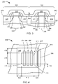
- FIG. 2 therein is shown a plan view of an integrated circuit 200 in an embodiment of the present invention.
- the plan view depicts an example of the integrated circuit 200 including memory systems 202 in a substrate 204 , such as a semiconductor substrate, wherein the substrate 204 may include one or more high-density core regions and one or more low-density peripheral portions are formed.
- High-density core regions typically include one or more of the memory systems 202 .
- Low-density peripheral portions typically include peripheral circuitry 210 , such as input/output (I/O) circuitry or transistors interfacing to the memory systems 202 , and programming circuitry for individually and selectively addressing a location in each of the memory systems 202 .
- peripheral circuitry 210 such as input/output (I/O) circuitry or transistors interfacing to the memory systems 202 , and programming circuitry for individually and selectively addressing a location in each of the memory systems 202 .
- the programming circuitry is represented in part by and includes one or more x-decoders 206 and y-decoders 208 , cooperating with the peripheral circuitry 210 for connecting the source, gate, and drain of selected addressed memory cells to predetermined voltages or impedances to effect designated operations on the memory cell, e.g. programming, reading, and erasing, and deriving necessary voltages to effect such operations.
- the integrated circuit 200 is shown as a memory device, although it is understood that the integrated circuit 200 may include other semiconductor devices having other functional blocks, such as a digital logic block, a processor, or other types of memories.
- the integrated circuit 200 includes the substrate 204 , such as a p-type substrate, having a first circuit element 312 , an isolation region 314 , a second circuit element 316 , a first stress formation liner 318 , such as a tensile layer of nitride or silicon nitride, and a second stress formation liner 320 , such as a compression layer of nitride or silicon nitride.
- the first stress formation liner 318 is preferably over the first circuit element 312 .
- the second stress formation liner 320 is preferably over the second circuit element 316 .
- the first circuit element 312 such as an n-type metal oxide semiconductor (NMOS) transistor, includes a first source 322 , such as an n-type source, formed in the substrate 204 .
- a first drain 324 such as an n-type drain, is formed in the substrate 204 .
- a first gate stack 326 is over the substrate 204 and over a first channel region 328 .
- the first channel region 328 is in the substrate 204 and between the first source 322 and the first drain 324 .
- An oxide liner 330 may be formed adjacent to the first gate stack 326 over the first source 322 and the first drain 324 .
- a first spacer 332 is preferably formed over the oxide liner 330 surrounding the first gate stack 326 as well as over the first source 322 and the first drain 324 .
- the second circuit element 316 such as a p-type metal oxide semiconductor (PMOS) transistor, includes a second source 334 formed in a well region 336 , such as an n-type well.
- the well region 336 is in the substrate 204 .
- a second drain 338 is formed in the well region 336 .
- a second gate stack 340 is preferably formed over the substrate 204 and over a second channel region 342 .
- the second channel region 342 is in the well region 336 located between the second source 334 and the second drain 338 .
- the oxide liner 330 is formed adjacent to the second gate stack 340 over the second source 334 and the second drain 338 .
- a second spacer 344 is formed on the oxide liner 330 surrounding the second gate stack 340 as well as over the second source 334 and the second drain 338 .
- the first stress formation liner 318 over the first circuit element 312 provides tensile stress to the first channel region 328 .
- This tensile stress strains the first channel region 328 to increase electron mobility thereby increasing performance, lowering power consumption, or a combination thereof of the first circuit element 312 .
- the second stress formation liner 320 over the second circuit element 316 provides compression stress to the second channel region 342 .
- This compression stress strains the second channel region 342 to increase hole mobility thereby increasing performance, lowering power consumption, or a combination thereof of the second circuit element 316 .
- the strain induced at the first circuit element 312 and the second circuit element 316 may not be limited to the stressed from the first stress formation liner 318 and the second stress formation liner 320 , respectively.
- the first stress formation liner 318 may also affect the strain at the second circuit element 316 .
- the second stress formation liner 320 may also affect the strain at the first circuit element 312 .
- Proximity of opposite type of stress liners can change the circuit element carrier effective mass properties depending on the distance of that opposite layer.
- compressive stress increases the hole mobility and makes the second circuit element 316 faster.
- Tensile stress in parallel direction reduces hole mobility at the second circuit element 316 .
- tensile stress in orthogonal direction increases hole mobility at the second circuit element 316 .
- the mobility increase and decrease are functions of distances of the stress source from the second circuit element 316 .
- the present invention provides equations for orthogonal and parallel directions for both NMOS and PMOS devices.
- the present invention further provides these equations and relationships in the compact model without the use of any other tools such as timing computer aided design (TCAD) modeling.
- TCAD timing computer aided design
- FIG. 4 therein is shown a more detailed plan view of a portion of the integrated circuit 200 of FIG. 3 .
- the plan view depicts the second circuit element 316 or the PMOS transistor, although it is understood that the following discussion may be appropriately applied to the first circuit element 312 of FIG. 3 with the first stress formation liner 318 of FIG. 3 .
- the second circuit element 316 also referred to as the device of interest or the victim device, includes an active area 402 .
- the active area 402 preferably includes the second source 334 of FIG. 3 and the second drain 338 of FIG. 3 under a first poly line 404 and a second poly line 406 , respectively.
- a gate line 408 is also over the active area 402 between the first poly line 404 and the second poly line 406 , wherein the gate line 408 is coupled to the second gate stack 340 of FIG. 3 .
- the second stress formation liner 320 is preferably over the active area 402 , the first poly line 404 , the second poly line 406 , and the gate line 408 .
- the gate line 408 , the first poly line 404 , and the second poly line 406 are shown as parallel structures to each other, although it is understood that the gate line 408 , the first poly line 404 , and the second poly line 406 may not be parallel to each other.
- the second stress formation liner 320 is shown in a rectangular shape. Also for example, the isolation region 314 is shown at a side 410 of the second stress formation liner 320 , although it is understood that the isolation region 314 may be located at other locations, such as under the second stress formation liner 320 , not adjacent to the second stress formation liner 320 , at other sides of the second stress formation liner 320 , or located at multiple locations with multiple instances.
- the active area 402 may be formed in a number of sizes and shapes.
- the active area 402 is shown in a rectangular shape having a length side 411 measured as an active length 412 denoted as “W rx ” and a width side 414 measured as an active width 416 denoted as “W”, wherein the length side 411 and the width side 414 are adjacent sides.
- the second stress formation liner 320 extends from the length side 411 a first distance 418 denoted as “dt 1 ” and from the opposite side to the length side 411 a second distance 420 denoted as “dt 2 ”.
- the second stress formation liner 320 extends from the width side 414 a third distance 422 denoted as “dl 1 ” and from the opposite side to the length side 411 a fourth distance 424 denoted as “dl 2 ”.
- FIG. 5 therein is shown the structure of FIG. 4 for modeling parallel stress.
- the modeling parallel stress may be included in the analysis block 103 of FIG. 1 .
- the characterization of the integrated circuit 200 preferably gathers numerous measurements for forming accurate models of the stress contribution upon a device element such as the second circuit element 316 .
- Equation 1 Stress, denoted as “ ⁇ ” at a distance “x” away from stress origin is proportional to 1/x and may be expressed generally as Equation 1:
- the parallel proximity component may be isolated by setting the first distance 418 of FIG. 4 , “dt 1 ”, and the second distance 420 of FIG. 4 , “dt 2 ”, to a sufficiently large value, for example greater than 5 ⁇ m, close to approximating the effect of an infinity value.
- the orthogonal proximity component may be isolated by setting the third distance 422 , “dl 1 ”, and the fourth distance 424 , “dl 2 ”, to a sufficiently large value, for example greater than 5 ⁇ m, close to approximating the effect of an infinity value.
- parallel stress sources 502 such as tensile sources, are preferably placed the third distance 422 , “dl 1 ”, and the fourth distance 424 , “dl 2 ” from the width side 414 of the active area 402 and the opposite side of the width side 414 of the active area 402 , respectively.
- the parallel stress sources 502 apply parallel proximity stress at the center of the second channel region 342 under the gate line 408 and may be expressed by Equation 2, based on Equation 1:
- ⁇ x ⁇ ⁇ 1 k x ⁇ ⁇ 1 [ ( 1 W rx 2 + dl 1 ) + ( 1 W rx 2 + dl 2 ) ] ( 2 )
- variable “k x1 ” may be a negative or positive value.
- FIG. 6 therein is shown the structure of FIG. 4 for modeling of parallel stress from the isolation region 314 .
- the modeling of parallel from the isolation region 314 may be included in the analysis block 103 of FIG. 1 .
- the isolation region 314 is shown parallel to the gate line 408 resulting in the isolation region 314 contributing to the parallel proximity component.
- the contribution of the isolation region 314 to the parallel proximity component may be modeled a number of ways.
- the parallel stress sources 502 may provide tensile stress at the first distance 418 of FIG. 4 and the second distance 420 of FIG. 4 has sufficiently large values.
- the parallel stress sources 502 may provide neutral stress as well as setting neutral stress to both the first stress formation liner 318 of FIG. 4 and the second stress formation liner 320 of FIG. 4 for isolating the effects from the isolation region 314 .
- the parallel proximity component from the isolation region 314 may be expressed as Equation 3 from evaluating Equation 2:
- the variable “k x2 ” may be a negative or positive value.
- orthogonal stress sources 702 such as tensile sources, are preferably placed the first distance 418 , “dt 1 ”, and the second distance 420 , “dt 2 ”, from the length side 411 of the active area 402 and the opposite side of the length side 411 of the active area 402 , respectively.
- the orthogonal stress will be different at different “y” or different locations from one of the orthogonal stress sources 702 .
- channel mobility will be enhanced or degraded differently at different values of “y” or different locations from the orthogonal stress sources 702 .
- the orthogonal proximity component may be expressed by integrating or averaging over the active width 416 , “W”.
- the orthogonal proximity component may be expressed by Equation 5:
- ⁇ y k y ⁇ ( 1 W ) ⁇ ln ⁇ [ ( 1 + W dt 1 ) ⁇ ( 1 + W dt 2 ) ] ( 5 )
- FIGS. 8A through 8E therein are shown plan views of orthogonal test structures for modeling the orthogonal stress of the structure of FIG. 4 .
- the orthogonal test structures preferably provide measurement device structures for providing the necessary information to evaluate Equation 6.
- I-V current-voltage
- a first orthogonal test structure 802 has the device of interest or in this example the second circuit element 316 under orthogonal stress from first test orthogonal sources 804 .
- the first test orthogonal sources 804 preferably exert tensile stress closest to the active area 402 compared to the other orthogonal test structures.
- a second orthogonal test structure 806 , a third orthogonal test structure 808 , a fourth orthogonal test structure 810 , and a fifth orthogonal test structure 812 preferably have second test orthogonal sources 814 , third test orthogonal sources 816 , fourth test orthogonal sources 818 , and fifth test orthogonal sources 820 , respectively, exerting tensile stress to its respective instantiation of the second circuit element 316 .
- five orthogonal test structures are shown for developing the orthogonal stress component, although it is understood that the number and types of orthogonal test structures may differ.
- the value of the first distance 418 , “dt 1 ”, and the second distance 420 , “dt 2 ” are increased.
- the first distance 418 and the second distance 420 are shown as equal and denoted by “dt” with the first orthogonal test structure 802 having “dt1”, the second orthogonal test structure 806 having “dt2”, the third test structure having “dt3”, the fourth orthogonal test structure 810 having “dt4”, and the fifth orthogonal test structure 812 having “dt5”.
- I deff ( I dhi + I dlow 2 ) ( 7 )
- Equation 7 for the orthogonal test structures is preferably plotted as function of “dt” from each of the orthogonal test structures.
- the value for “dt5” of the fifth orthogonal test structure 812 is preferably sufficiently large such that Equation 5 may be evaluated as: ⁇ y (dt5) ⁇ 0. (8)
- I deff is preferably measured at same I off which means that the enhancement/degradation at different “dt” stems from stress induced mobility change in the channel.
- the fifth orthogonal test structure 812 is preferably used for normalizing the measured currents and tabulated in Table 1 below.
- FIG. 9 therein is shown a graphical view of a plot 902 of the orthogonal test structures of FIG. 8A through 8E .
- the plot 902 may be provided by the presentation block 104 of FIG. 1 .
- the plot 902 depicts the values from Table 1 above with a curve 904 as estimated values.
- the x-axis represents “dt” and the y-axis represents the normalized ratio of ⁇ I deff /I deff from the second column of Table 1.
- I deff in the second circuit element 316 of FIG. 3 , the PMOS device, or in the first circuit element 312 of FIG. 3 , the NMOS device, respectively, with orthogonal distance is from the change in mobility.
- the increase or decrease in I deff normalized to I deff of the fifth orthogonal test structure 812 of FIG. 8E is proportional to mobility increase (decrease) normalized to mobility of the fifth orthogonal test structure 812 .
- ⁇ I deff /I deff5 is evaluated as ⁇ y expressed by Equation 8.
- Equation 9 The relationship between ⁇ y and mobility is expressed by Equation 9:
- Equation 9 The mobility of each of the orthogonal test structures is denoted as ⁇ eff and the reference test structure or the fifth test structure is denoted as ⁇ eff0 .
- Equation 9 Relating Equation 9 with Equation 5, “k y ” may be extracted from measured currents from the orthogonal test structures and preferably used for forming the compact model in the analysis block 103 of FIG. 1 .
- FIGS. 10A through 10E therein are shown plan views of parallel test structures for modeling the parallel stress of the structure of FIG. 4 .
- “k x1 ” may be preferably extracted or derived from measured current for the compact model in the analysis block 103 of FIG. 1 and the measured current may be from the extraction block 102 of FIG. 1 .
- the parallel test structures vary from one another by varying the value of the third distance 422 , “dl 1 ”, and the fourth distance 424 , “dl 2 ”, from the active area 402 with other variables fixed.
- a first parallel test structure 1002 has the device of interest or in this example the second circuit element 316 under parallel stress from first test parallel sources 1004 .
- the first test parallel sources 1004 preferably exert tensile stress closest to the active area 402 compared to the other parallel test structures for parallel stress.
- a second parallel test structure 1006 , a third parallel test structure 1008 , a fourth parallel test structure 1010 , and a fifth parallel test structure 1012 preferably have second test parallel sources 1014 , third test parallel sources 1016 , fourth test parallel sources 1018 , and fifth test parallel sources 1020 , respectively, exerting tensile stress to its respective instantiation of the second circuit element 316 .
- the value of the third distance 422 , “dl 1 ”, and the fourth distance 424 , “dl 2 ” are increased.
- the third distance 422 and the fourth distance 424 are shown as equal and denoted by “dl” with the first parallel test structure 1002 having “dl1”, the second parallel test structure 1006 having “dl2”, the third test structure having “dl3”, the fourth parallel test structure 1010 having “dl4”, and the fifth parallel test structure 1012 having “dl5”.
- the fifth parallel test structure 1012 may be used to provide a normalized value and forming a similar table to Table 1 above. The process may continue similarly as for the orthogonal test structures for extracting “k x1 ”.
- FIGS. 11A through 11E are plan views of trench test structures for modeling the stress from the isolation region 314 of the structure of FIG. 4 . Similar to “k y ” and “k x1 ”, “k x2 ” may be preferably extracted or derived from measured current for the compact model in the analysis block 103 of FIG. 1 and the measured current is preferably from the extraction block 102 of FIG. 1 .
- the trench test structures vary from one another by varying the value of the active length 412 of FIG. 3 , “W rx ”, of the active area 402 of FIG. 3 of the second circuit element 316 of FIG. 3 with other variables fixed.
- a first trench test structure 1102 has the device of interest or in this example a first test circuit element 1104 under parallel stress from trench parallel sources 1106 .
- the first test circuit element 1104 has a first active area 1108 with a first active length 1110 denoted as “W rx1 ”.
- the first test circuit element 1104 is similar to the second circuit element 316 with both having compressive stress over the first active area 1108 and the active area 402 , respectively.
- the first trench test structure 1102 has the first active area 1108 furthest from the trench parallel sources 1106 compared with the other trench test structures, wherein the trench parallel sources 1106 preferably exert tensile stress to the first active area 1108 .
- a second trench test structure 1112 , a third trench test structure 1114 , a fourth trench test structure 1116 , and a fifth trench test structure 1118 preferably have a second active area 1120 , a third active area 1122 , a fourth active area 1124 , and a fifth active area 1126 , respectively, with the trench parallel sources 1106 exerting tensile stress to its respective active area.
- the second active area 1120 includes a second active length 1128 denoted as “W rx2 ” with the second active length 1128 greater than the first active length 1110 .
- the third active area 1122 includes a third active length 1130 denoted as “W rx3 ” with the third active length 1130 greater than the second active length 1128 .
- the fourth active area 1124 includes a fourth active length 1132 denoted as “W rx4 ” with the fourth active length 1132 greater than the third active length 1130 .
- the fifth active area 1126 includes a fifth active length 1134 denoted as “W rx5 ” with the fifth active length 1134 greater than the fourth active length 1132 .
- the fifth trench test structure 1118 may be used to provide a normalized value and forming a similar table to Table 1 above.
- the device of interest (DOI) or the second circuit element 316 with fixed proximities, “W rx ”, “W”, etc.
- the mobility ( ⁇ 0 ) for this particular device referred to as a reference device, will be extracted based on I-V characteristics.
- the other proximity affects mobility.
- the reference device has proximity parameters “dt 0 ”, “dl 0 ”, “W 0 ”, and “W rx0 ”.
- the device of interest has proximity parameters “dt”, “dl”, “W”, and “W rx ”.
- the mobility for the device of interest may be expressed in Equation 12:
- a smart phone 1202 , a satellite 1204 , and a computer system 1206 are examples of the electronic systems using the present invention.
- the electronic systems may be any system that performs any function for the creation, transportation, storage, and consumption of information.
- the smart phone 1202 may create information by transmitting voice to the satellite 1204 .
- the satellite 1204 is used to transport the information to the computer system 1206 .
- the computer system 1206 may be used to store the information.
- the smart phone 1202 may also consume information sent from the satellite 1204 .
- the electronic systems such as the smart phone 1202 , the satellite 1204 , and the computer system 1206 , include a one or more subsystem, such as a printed circuit board having the present invention or an electronic assembly having the present invention.
- the electronic system may also include a subsystem, such as an adapter card.
- the method 1300 includes measuring current information from test structures for an integrated circuit having dual stress liners in a block 1302 ; selecting currents from the current information or stored current information in a block 1304 ; deriving a scaling factor with the currents for a stress contribution based on an active area of a circuit element in the integrated circuit in a block 1306 ; and correlating the stress contribution with the integrated circuit in a block 1308 .
- the integrated circuit tester information processing system method and apparatus of the present invention furnish important and heretofore unknown and unavailable solutions, capabilities, and functional aspects for memory systems.
- the resulting processes and configurations are straightforward, cost-effective, uncomplicated, highly versatile, accurate, sensitive, and effective, and can be implemented by adapting known components for ready, efficient, and economical manufacturing, application, and utilization.
Abstract
Description
σx=σx1+σx2 (4)
σchannel=σx+σy=σx1+σx2+σy (6)
σy(dt5)˜0. (8)
| Test Structure Number | ΔIdeff/Ideff |
| 1 | (Ideff1 − Ideff5)/Ideff5 |
| 2 | (Ideff2 − Ideff5)/Ideff5 |
| 3 | (Ideff3 − Ideff5)/Ideff5 |
| 4 | (Ideff4 − Ideff5)/Ideff5 |
| 5 | (Ideff5 − Ideff5)/Ideff5 = 0 |
σ0=σx0+σy0 (10)
σ=σx+σy (11)
Claims (20)
Priority Applications (1)
| Application Number | Priority Date | Filing Date | Title |
|---|---|---|---|
| US11/857,272 US7610160B2 (en) | 2007-09-18 | 2007-09-18 | Integrated circuit tester information processing system |
Applications Claiming Priority (1)
| Application Number | Priority Date | Filing Date | Title |
|---|---|---|---|
| US11/857,272 US7610160B2 (en) | 2007-09-18 | 2007-09-18 | Integrated circuit tester information processing system |
Publications (2)
| Publication Number | Publication Date |
|---|---|
| US20090076750A1 US20090076750A1 (en) | 2009-03-19 |
| US7610160B2 true US7610160B2 (en) | 2009-10-27 |
Family
ID=40455479
Family Applications (1)
| Application Number | Title | Priority Date | Filing Date |
|---|---|---|---|
| US11/857,272 Expired - Fee Related US7610160B2 (en) | 2007-09-18 | 2007-09-18 | Integrated circuit tester information processing system |
Country Status (1)
| Country | Link |
|---|---|
| US (1) | US7610160B2 (en) |
Citations (5)
| Publication number | Priority date | Publication date | Assignee | Title |
|---|---|---|---|---|
| US20040149045A1 (en) | 2001-12-07 | 2004-08-05 | Johnson Mont A. | Apparatus and method for measuring stress at an interface |
| US7101744B1 (en) | 2005-03-01 | 2006-09-05 | International Business Machines Corporation | Method for forming self-aligned, dual silicon nitride liner for CMOS devices |
| US20070028195A1 (en) | 2005-07-29 | 2007-02-01 | International Business Machines Corporation | Methodology for layout-based modulation and optimization of nitride liner stress effect in compact models |
| US20090099829A1 (en) * | 2007-10-15 | 2009-04-16 | Advanced Micro Devices, Inc. | Integrated circuit tester information processing system for nonlinear mobility model for strained device |
| US20090113368A1 (en) * | 2007-10-26 | 2009-04-30 | Synopsys, Inc. | Filler cells for design optimization in a place-and-route system |
-
2007
- 2007-09-18 US US11/857,272 patent/US7610160B2/en not_active Expired - Fee Related
Patent Citations (5)
| Publication number | Priority date | Publication date | Assignee | Title |
|---|---|---|---|---|
| US20040149045A1 (en) | 2001-12-07 | 2004-08-05 | Johnson Mont A. | Apparatus and method for measuring stress at an interface |
| US7101744B1 (en) | 2005-03-01 | 2006-09-05 | International Business Machines Corporation | Method for forming self-aligned, dual silicon nitride liner for CMOS devices |
| US20070028195A1 (en) | 2005-07-29 | 2007-02-01 | International Business Machines Corporation | Methodology for layout-based modulation and optimization of nitride liner stress effect in compact models |
| US20090099829A1 (en) * | 2007-10-15 | 2009-04-16 | Advanced Micro Devices, Inc. | Integrated circuit tester information processing system for nonlinear mobility model for strained device |
| US20090113368A1 (en) * | 2007-10-26 | 2009-04-30 | Synopsys, Inc. | Filler cells for design optimization in a place-and-route system |
Non-Patent Citations (1)
| Title |
|---|
| C.D. Sheraw et al., Dual Stress Liner Enhancement in Hybrid Orientation Technology, 2005 Symposium on VLSI Technology Digest of Technical Papers, pp. 12-13. |
Also Published As
| Publication number | Publication date |
|---|---|
| US20090076750A1 (en) | 2009-03-19 |
Similar Documents
| Publication | Publication Date | Title |
|---|---|---|
| US10790281B2 (en) | Stacked channel structures for MOSFETs | |
| US7093215B2 (en) | Semiconductor circuit device and circuit simulation method for the same | |
| US8407634B1 (en) | Analysis of stress impact on transistor performance | |
| US7802218B2 (en) | Layout analysis method and apparatus for semiconductor integrated circuit | |
| Mishra et al. | Die-level leakage power analysis of FinFET circuits considering process variations | |
| US7462914B2 (en) | Semiconductor circuit device and simulation method of the same | |
| Koneru et al. | Analysis of electrostatic coupling in monolithic 3D integrated circuits and its impact on delay testing | |
| US7630850B2 (en) | Integrated circuit tester information processing system for nonlinear mobility model for strained device | |
| US8818785B2 (en) | Method and apparatus for simulating gate capacitance of a tucked transistor device | |
| US7617065B2 (en) | Methodology for estimating statistical distribution characteristics of physical parameters of semiconductor device | |
| Sukharev et al. | 3D IC TSV‐Based Technology: Stress Assessment For Chip Performance | |
| US7610160B2 (en) | Integrated circuit tester information processing system | |
| US20160099239A1 (en) | Methods, apparatus and system for reduction of power consumption in a semiconductor device | |
| Sukharev et al. | Multi-scale simulation methodology for stress assessment in 3D IC: effect of die stacking on device performance | |
| US20130117002A1 (en) | Method and Apparatus for Simulating Junction Capacitance of a Tucked Transistor Device | |
| Sinha et al. | Circuit design perspectives for Ge FinFET at 10nm and beyond | |
| Badaroglu et al. | More Moore landscape for system readiness-ITRS2. 0 requirements | |
| TWI626551B (en) | Method of designing fin-based transistor for power optimization | |
| CN109841613B (en) | Generating a model of a dynamically depleted transistor using a system with analog circuitry | |
| JP4753495B2 (en) | Integrated circuit design evaluation method, apparatus, and program | |
| Xu et al. | Investigation of 65 nm CMOS transistor local variation using a FET array | |
| US8296701B2 (en) | Method for designing a semiconductor device based on leakage current estimation | |
| US7932103B2 (en) | Integrated circuit system with MOS device | |
| US20220415812A1 (en) | Local density control for metal capacitance reduction | |
| CN109979843B (en) | Apparatus and method for verifying pattern shifts in a layout |
Legal Events
| Date | Code | Title | Description |
|---|---|---|---|
| AS | Assignment |
Owner name: ADVANCED MICRO DEVICES, INC., CALIFORNIA Free format text: ASSIGNMENT OF ASSIGNORS INTEREST;ASSIGNORS:SURYAGANDH, SUSHANT S.;AN, JUDY XILIN;REEL/FRAME:019844/0561;SIGNING DATES FROM 20070911 TO 20070912 |
|
| AS | Assignment |
Owner name: GLOBALFOUNDRIES INC., CAYMAN ISLANDS Free format text: AFFIRMATION OF PATENT ASSIGNMENT;ASSIGNOR:ADVANCED MICRO DEVICES, INC.;REEL/FRAME:023120/0426 Effective date: 20090630 Owner name: GLOBALFOUNDRIES INC.,CAYMAN ISLANDS Free format text: AFFIRMATION OF PATENT ASSIGNMENT;ASSIGNOR:ADVANCED MICRO DEVICES, INC.;REEL/FRAME:023120/0426 Effective date: 20090630 |
|
| STCF | Information on status: patent grant |
Free format text: PATENTED CASE |
|
| FPAY | Fee payment |
Year of fee payment: 4 |
|
| FPAY | Fee payment |
Year of fee payment: 8 |
|
| AS | Assignment |
Owner name: WILMINGTON TRUST, NATIONAL ASSOCIATION, DELAWARE Free format text: SECURITY AGREEMENT;ASSIGNOR:GLOBALFOUNDRIES INC.;REEL/FRAME:049490/0001 Effective date: 20181127 |
|
| AS | Assignment |
Owner name: GLOBALFOUNDRIES U.S. INC., CALIFORNIA Free format text: ASSIGNMENT OF ASSIGNORS INTEREST;ASSIGNOR:GLOBALFOUNDRIES INC.;REEL/FRAME:054633/0001 Effective date: 20201022 |
|
| AS | Assignment |
Owner name: GLOBALFOUNDRIES INC., CAYMAN ISLANDS Free format text: RELEASE BY SECURED PARTY;ASSIGNOR:WILMINGTON TRUST, NATIONAL ASSOCIATION;REEL/FRAME:054636/0001 Effective date: 20201117 |
|
| AS | Assignment |
Owner name: GLOBALFOUNDRIES U.S. INC., NEW YORK Free format text: RELEASE BY SECURED PARTY;ASSIGNOR:WILMINGTON TRUST, NATIONAL ASSOCIATION;REEL/FRAME:056987/0001 Effective date: 20201117 |
|
| FEPP | Fee payment procedure |
Free format text: MAINTENANCE FEE REMINDER MAILED (ORIGINAL EVENT CODE: REM.); ENTITY STATUS OF PATENT OWNER: LARGE ENTITY |
|
| LAPS | Lapse for failure to pay maintenance fees |
Free format text: PATENT EXPIRED FOR FAILURE TO PAY MAINTENANCE FEES (ORIGINAL EVENT CODE: EXP.); ENTITY STATUS OF PATENT OWNER: LARGE ENTITY |
|
| STCH | Information on status: patent discontinuation |
Free format text: PATENT EXPIRED DUE TO NONPAYMENT OF MAINTENANCE FEES UNDER 37 CFR 1.362 |
|
| FP | Lapsed due to failure to pay maintenance fee |
Effective date: 20211027 |