US7587550B2 - Functional test method and functional test apparatus for data storage devices - Google Patents
Functional test method and functional test apparatus for data storage devices Download PDFInfo
- Publication number
- US7587550B2 US7587550B2 US11/544,914 US54491406A US7587550B2 US 7587550 B2 US7587550 B2 US 7587550B2 US 54491406 A US54491406 A US 54491406A US 7587550 B2 US7587550 B2 US 7587550B2
- Authority
- US
- United States
- Prior art keywords
- data
- storage device
- data storage
- address
- write
- Prior art date
- Legal status (The legal status is an assumption and is not a legal conclusion. Google has not performed a legal analysis and makes no representation as to the accuracy of the status listed.)
- Expired - Fee Related, expires
Links
- 238000013500 data storage Methods 0.000 title claims abstract description 67
- 238000011990 functional testing Methods 0.000 title claims abstract description 53
- 238000000034 method Methods 0.000 title claims description 26
- 238000012360 testing method Methods 0.000 claims abstract description 56
- 230000015654 memory Effects 0.000 claims abstract description 38
- 238000010586 diagram Methods 0.000 description 12
- 230000006870 function Effects 0.000 description 3
- 230000005540 biological transmission Effects 0.000 description 2
- 230000002950 deficient Effects 0.000 description 2
- 230000006978 adaptation Effects 0.000 description 1
- 230000001419 dependent effect Effects 0.000 description 1
- 230000000694 effects Effects 0.000 description 1
- 239000000835 fiber Substances 0.000 description 1
- 230000003287 optical effect Effects 0.000 description 1
Images


Classifications
-
- G—PHYSICS
- G06—COMPUTING; CALCULATING OR COUNTING
- G06F—ELECTRIC DIGITAL DATA PROCESSING
- G06F13/00—Interconnection of, or transfer of information or other signals between, memories, input/output devices or central processing units
- G06F13/38—Information transfer, e.g. on bus
- G06F13/382—Information transfer, e.g. on bus using universal interface adapter
- G06F13/385—Information transfer, e.g. on bus using universal interface adapter for adaptation of a particular data processing system to different peripheral devices
Definitions
- the present invention relates to a functional test method and functional test apparatus for data storage devices.
- HDD hard disk drive
- the hard disk drive has become so popular as to be one of the indispensable storage devices for today's computer systems.
- the hard disk drive is widening its range of application more and more due to the superior characteristics, covering moving picture recording/reproducing apparatus, car navigation systems, removable memories for digital cameras and so on.
- FIG. 10 Shown in FIG. 10 is a typical PC-used functional test method for an HDD.
- a PC 91 and an HBA (Host Bus Adapter) 92 are used.
- the HBA 92 is connected with an HDD 93 by a cable 94 .
- a memory 911 , a PCI bus bridge 912 and a CPU 913 which are provided in the PC 91 are respectively connected to a CPU bus 914 .
- the HBA 92 has an interface controller 921 provided therein.
- Write data 931 is prepared in the memory 911 such as a DRAM. In addition, an area is reserved for read data 932 .
- the CPU 913 sends a write instruction to the HDD 93 .
- the HDD 93 instructs the PCI bus 915 to send desired data.
- the write data 931 in the memory 911 is sent to the interface controller 921 via the PCI bus bridge 912 .
- the interface controller 921 sends the write data 931 to the HDD 93 according to the interface of the HDD 93 .
- the HDD 93 writes/stores the write data 931 .
- the CPU 913 After a signal indicating that the data is written in the HDD 93 is sent from the HDD 93 , the CPU 913 sends a read instruction to the HDD 93 .
- the interface controller 921 receives the read data 932 from the HDD 93 according to the HDD interface.
- the read data 932 from the interface controller 921 is written in the memory 911 by the PCI bus bridge 912 .
- the CPU 913 compares the write data 931 in the memory 911 with the read data 932 therein.
- FIG. 11 Shown in FIG. 11 is such a functional test method for HDDs.
- a CPU board 95 is used in place of a PC and an interface board 96 is used in place of an HBA.
- a memory 951 such as a DRAM
- a PCI bus bridge 952 and a CPU 953 are provided in the CPU board 95 .
- the memory 951 , the PCI bus bridge 952 and the CPU 953 are respectively connected to a CPU bus 954 .
- the PCI bus bridge 952 has a data comparator circuit provided therein.
- the interface board 96 has an interface controller 961 provided therein.
- the PCI bus bridge 952 in the CPU board 95 and the interface controller 961 in the interface board 96 are connected to the PCI bus 955 .
- the interface board 96 and the HDD 93 are connected by an HDD interface 962 .
- Write data 931 is prepared in the memory 951 such as a DRAM.
- the CPU 953 sends a write instruction to the HDD 93 .
- the HDD 93 sends an instruction to the PCI bus 956 to instruct it to send desired data. Then, the write data 931 in the memory 911 is sent to the interface controller 961 via the PCI bus bridge 952 .
- the interface controller 961 sends the write data 931 to the HDD 93 according to the HDD interface 962 .
- the HDD 93 writes/stores the write data 931 .
- the CPU 953 sends a read instruction to the HDD 93 .
- the interface controller 961 receives the read data from the HDD 93 according to the HDD interface 962 .
- the PCI bus bridge 952 reads the write data 931 from the memory 951 and compares it with the read data from the interface controller 961 .
- the CPU 953 obtains the comparison result from the PCI bus bridge 952 .
- the present invention was made in order to solve the above-mentioned problem. It is a feature of the present invention to provide a high speed functional test apparatus for HDDs by increasing the amount of data to be transferred per command without using a larger memory resource.
- a data storage device functional test apparatus comprising a storage section to store original data; a data generating section which generates transfer data, larger in size than the original data, for each command to a data storage device by repeatedly using the original data; and a transfer section which transfers the generated transfer data to the data storage device. Since the transfer data size per CPU command can be increased by repeatedly using the original data, it is possible to substantially reduce the time spent to test the function of a data storage device without increasing the capacity of the memory.
- the data generating section generates the transfer data by using the original data and variable data which varies depending on the address in the data storage device.
- each transfer data comprises original data and variable data
- different data is written to each address in the data storage device.
- a value associated with a specific address in the data storage device is used as the variable data. Such a value may be generated by a counter. It is also preferable to generate different variable data for each sector.
- a “sector” is the data storage device's smallest unit of storage.
- the variable data it is also preferable to use an address in the data storage device associated with the variable data.
- the above-mentioned data storage functional test apparatus is further provided with a comparator circuit.
- Write operation is done to an address in the data storage device and, after that, read operation is done from the address in the data storage device; a comparator circuit is further provided.
- the comparator circuit By the comparator circuit, the write data which the write operation tried to write to the address is compared with the read data which is read from the address by the read operation.
- the data generating section to generate write data which is associated with an address from which the read operation is to be done, allowing the comparator circuit to compare the read data read from the address with the write data associated with the address.
- a data storage device functional test method comprising the steps of: by repeatedly using original data, generating transfer data larger in size than the original data; performing a write operation by transferring the transfer data to a data storage device; after the write operation is complete, performing a read operation from the data storage device; and comparing the read data which is read from an address with the write data which the write operation tried to write to the address.
- the HDD functional test apparatus can reduce the test time by transferring large data without using a high speed and large capacity memory since small data stored in an HDD testing ASIC is used repeatedly.
- FIG. 1 is a block diagram of an HDD functional test apparatus configured according to an embodiment of the invention.
- FIG. 2 is a detailed block diagram of the HDD testing ASIC.
- FIG. 3 is a first schematic diagram showing signal flows in the HDD testing ASIC.
- FIG. 4 is a second schematic diagram showing signal flows in the HDD testing ASIC.
- FIG. 5 is a third schematic diagram showing signal flows in the HDD testing ASIC.
- FIG. 6 is a fourth schematic diagram showing signal flows in the HDD testing ASIC.
- FIG. 7 is a fifth schematic diagram showing signal flows in the HDD testing ASIC.
- FIG. 8 is a sixth schematic diagram showing signal flows in the HDD testing ASIC.
- FIG. 9 is a test time comparison table for the HDD functional test apparatus according to the embodiment of the invention.
- FIG. 10 shows a block diagram of a conventional HDD functional test apparatus which uses a PC.
- FIG. 11 shows a block diagram of a conventional HDD functional test apparatus where no PC is used.
- the present embodiment assumes an HDD.
- This functional test method performs error check by writing data to the whole disk surface, reading data from the disk and comparing read data with write data for each address.
- the data storage device functional test apparatus generates write data for each address to which data is to be written.
- Each write data is generated by using original data which is common to all addresses and variable data which varies depending on the address to which the data is to be written.
- the HDD functional test method can transfer larger size data than the original data by one command since write data is generated by repeatedly using original data. This makes it possible to transfer large data without needing a large memory. Since it is possible to increase the amount of data to be transferred per command, it is possible to decrease the number of commands in the functional test of an HDD and therefore drastically decrease the time spent in the functional test of the HDD.
- the HDD functional test method according to the present embodiment uses a testing CPU board instead of a PC and an interface board instead of an HBA.
- a PCI bus bridge provides a bridge between a CPU bus to which a CPU is connected and a PCI bus to which the interface board is connected.
- the PCI bus bridge implements the HDD functional test method according to the present invention.
- Use of the HDD testing ASIC to integrate the PCI bus bridge therein makes it possible to add new functions to the PCI bus bridge without mounting additional chips.
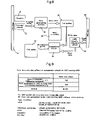
- FIG. 1 shows a block diagram of an HDD functional test apparatus configured according to the present embodiment.
- a CPU board 11 has a memory 111 such as a DRAM and a CPU 112 provided therein.
- the memory 111 and the CPU 112 are connected by a CPU bus 14 .
- a PCI bus 16 exists between the CPU board 11 and an interface board 12 .
- a PCI bus bridge 15 is provided as a bridge between the CPU bus 14 and the PCI bus 16 .
- This PCI bus bridge 15 is implemented by an HDD testing ASIC 151 .
- An interface board 12 has an interface controller 121 provided therein. This interface controller 121 is connected to the PCI bus bridge 15 in the CPU board 11 via the PCI bus 16 . In addition, an HDD interface 17 is disposed between the interface board 12 and an HDD 13 .
- the CPU 112 initially sends a write command to the HDD 13 via the CPU bus 14 , the PCI bus bridge 15 , the PCI bus 16 and the interface board 12 .
- the HDD 13 Upon getting ready to write the data which is to be sent following the write command, the HDD 13 sends a signal to the HDD testing ASIC 151 via the interface board 12 to indicate that it is ready to receive the write data for performing a write operation.
- the HDD testing ASIC 151 When the write command, issued from the CPU 112 to the HDD 13 , goes through the PCI bridge 15 , it is received by the HDD testing ASIC 151 .
- the HDD testing ASIC 151 transfers the write data. This write data is created in the HDD testing ASIC 151 and transferred through the PCI bus 16 to the HDD 13 for write therein.
- the HDD 13 sends a signal to the CPU 112 to indicate that the data is sent. By repeating this, write is done to the whole disk surface in the HDD 13 .
- disk read operation is performed.
- the CPU 112 initially sends a read command to the HDD 13 via the CPU bus 14 , the PCI bus bridge 15 , the PCI bus 16 and the interface board 12 .
- Data, read in the HDD 13 is sent to the HDD testing ASIC 151 via the interface board 12 and the PCI bus 16 .
- error check is performed through data comparison for each read address. If an error is detected, the address which caused the error is stored in the buffer in the HDD testing ASIC 151 .
- FIG. 2 shows a detailed block diagram of the HDD testing ASIC 151 .
- the PCI bus bridge 15 containing the HDD testing circuit is shown with the CPU bus 14 and the PCI bus 16 .
- the HDD testing ASIC 151 there are provided: a register 21 which stores original data; a counter circuit 22 which generates a counter value; a data generating section 23 which generates write data by using a counter value from the counter circuit 22 and original data from the register 21 ; a first buffer 24 which temporally stores write data generated by the data generating section 23 and a command entered via the CPU bus 14 and sends them as timed by the PCI bus clock; and a main controller 25 which controls data transmission and reception timings in the HDD testing ASIC 151 .
- the HDD testing ASIC contains: a comparator circuit 26 which compares write data having been put under write operation with the corresponding read data read from the HDD; a second buffer 27 which stores a comparison result from the comparator circuit 26 ; a data transfer judgment circuit 28 which transfers data from the PCI bus 16 to the comparator circuit 26 or the second buffer 27 . To which of them the data from the PCI bus is to be transferred by the data transfer judgment circuit 28 is controlled by the main controller 25 in the HDD testing ASIC 151 .
- the data generating section 23 generates write data by using variable data which is disk address-dependent and original data which is stored in the data generating section 23 .
- a counter value from the counter circuit 22 is used as variable data. This is because a counter value is associated one by one with write data and a disk address at which the write data is written.
- write data is written at the same disk address as the counter value since this eliminates the necessity of storing the counter value to disk address associations in the memory. Also preferably, the size of each write data is made equal to the amount of data per sector since this makes it easy to associate addresses with counter values.
- the data generating section 23 repeatedly generates one write data for transmission to the HDD 13 each time a write command is executed.
- each write data contains variable data which varies depending on the counter value. Thus, different data can be written at each address. In addition, this makes it possible for the main controller to control the amount of data to be transferred per command.
- FIGS. 3 , 4 , 5 , 6 , 7 and 8 schematically show how the above-mentioned apparatus performs functional testing of the HDD 13 .
- a write command from the CPU 112 is sent to the HDD 13 via the CPU bus 14 , the first buffer 24 in the PCI bus bridge 15 (HDD testing ASIC 151 ), the PCI bus 16 and the interface board 12 .
- the write command is also sent to the main controller 25 (see FIG. 3 ).
- the HDD 13 Upon getting ready to write data which is to be sent following the write command, the HDD 13 sends a signal to the main controller 25 in the HDD testing ASIC 151 to indicate that it is ready to receive the write data (see FIG. 4 ).
- the main controller 25 sends a data generation start signal to the data generating section 23 .
- the data generating section 23 reads a write data amount from the register 21 and a counter value from the counter circuit 22 . After the counter value is fetched by the data generating section 23 , the counter circuit 22 increments the counter value by 1.
- the data generating section 23 generates write data by using the original data having been stored therein via the CPU bus 14 and the counter value from the counter circuit 22 (see FIG. 5 ).
- the generated write data is stored in the buffer 24 and sent to the PCI bus 16 by the PCI bus clock. This action is repeated until the amount of transferred data reaches the data amount given from the main controller 25 .
- a counter value to write address association table is created in advance by the main controller 25 and stored in an internal memory thereof. Alternatively, this association table may be stored in a memory which is prepared separately from the main controller 25 and the register 21 . This memory must not be too large since the association table does not contain much data. In addition, this association table is not necessary if the counter value is taken as the disk address to which the write data is to be written.
- a write completion signal is issued from the HDD 13 (see FIG. 6 ).
- read operation is performed.
- the CPU 112 sends a read command to the HDD 13 via the CPU bus 14 , the first buffer 24 , the PCI bus 15 and the interface board 12 (see FIG. 7 ).
- the main controller 25 sends a data generation start signal to the data generating section 23 .
- the data generating section 23 reads a data transfer amount from the register 21 and a counter value from the counter circuit 22 . Then, the data generating section 23 fetches the original data to generate write data which was written to the address from which data is being read (see FIG. 8 ).
- the data generating section 23 sends this generated write data to the first buffer 24 .
- the first buffer 24 sends this generated write data to the comparator circuit 26 by the PCI bus clock.
- the data read from the HDD 13 is sent through the interface board 12 to the PCI bus 16 .
- the PCI address for the read data sent to the PCI bus 16 is sent to the data transfer judgment circuit 28 .
- the data transfer judgment circuit 28 determines to which of the comparator circuit 26 and the second buffer 27 the data is to be transferred. According to the judgment result, the data from the PCI bus 16 is transferred to the comparator circuit 26 .
- the data read from the HDD 13 is sent to the comparator circuit 26 by the data transfer judgment circuit 28 .
- the write data from the first buffer 24 and the read data from the data transfer judgment circuit 28 are entered into the comparator circuit 26 .
- the comparator circuit 26 compared the entered read data with the entered write data. If the comparison result shows no difference, HDD functional testing for this address is complete since the addressed location is normal in the HDD 13 .
- the read data for this address is sent to the second buffer 27 and stored therein since the addressed location in the HDD 13 is defective. Alternatively, this data may be sent from the second buffer 27 to the memory 111 via the CPU bus 14 . From this data registered at the memory 111 , an alternate sector may be prepared for use when the defective address is tried to be accessed for read or write.
- a table in FIG. 9 shows test results.
- the tested HDD was HITACHI GST 18GB FC-2GB HDD (IC35L018F2DY10-0). This HDD was tested by using q'logic Corporation ISP 2300 as the interface controller, HITACHI (Renesas) SH-3 56.75 MHz as the CPU, GreenHills C Compiler and a 64BIT/56.75 MHz PCI bus.
- test conditions are shown in the left column of the FIG. 9 table.
- test times spent are shown in the right column of the table.
- memory was used to transfer data.
- data was generated in the HDD testing ASIC.
- 496 sectors were transferred per command.
- FFFFh sectors were transferred per command, data was generated in the HDD testing ASIC according to the present invention.
- the “Effect” row the result of the memory transfer-based test is compared with the result of the test according to the present invention.
- the test time can be reduced to about a half as compared with the memory transfer-based test.
- this method uses only a very small memory area. By increasing the amount of data transferred per command, it is therefore possible to realize an HDD functional test which can be performed quickly by using a small memory resource.
- the present invention is not limited to the above-mentioned embodiment. Needless to say, various changes may be made thereunto without departing from the spirit of the present invention.
- the above-described embodiment assumes an HDD
- the present invention is applicable to other data storage devices.
- read operation is performed after write operation is completed for the whole disk surface in the above-mentioned HDD function test, write operation and read operation may be done consecutively for each predetermined area.
Abstract
Description
Claims (17)
Applications Claiming Priority (2)
| Application Number | Priority Date | Filing Date | Title |
|---|---|---|---|
| JP2005-294305 | 2005-10-07 | ||
| JP2005294305A JP2007102653A (en) | 2005-10-07 | 2005-10-07 | Method and apparatus for testing function of data storage apparatus |
Publications (2)
| Publication Number | Publication Date |
|---|---|
| US20070083705A1 US20070083705A1 (en) | 2007-04-12 |
| US7587550B2 true US7587550B2 (en) | 2009-09-08 |
Family
ID=37912143
Family Applications (1)
| Application Number | Title | Priority Date | Filing Date |
|---|---|---|---|
| US11/544,914 Expired - Fee Related US7587550B2 (en) | 2005-10-07 | 2006-10-05 | Functional test method and functional test apparatus for data storage devices |
Country Status (3)
| Country | Link |
|---|---|
| US (1) | US7587550B2 (en) |
| JP (1) | JP2007102653A (en) |
| CN (1) | CN100517259C (en) |
Families Citing this family (7)
| Publication number | Priority date | Publication date | Assignee | Title |
|---|---|---|---|---|
| US7707468B2 (en) * | 2007-03-22 | 2010-04-27 | Verigy (Singapore) Pte. Ltd | System and method for electronic testing of multiple memory devices |
| US20080235542A1 (en) * | 2007-03-22 | 2008-09-25 | Duncan Gurley | Electronic testing device for memory devices and related methods |
| JP5266713B2 (en) * | 2007-10-23 | 2013-08-21 | 日本電気株式会社 | Information processing apparatus, program, external encryption system, and external encryption method |
| TWI384357B (en) * | 2008-10-31 | 2013-02-01 | Inventec Corp | System and method for testing bridge sas channels |
| US8769188B2 (en) * | 2009-11-18 | 2014-07-01 | Mediatek Inc. | Nonvolatile memory controller and method for writing data to nonvolatile memory |
| TW201504650A (en) * | 2013-07-19 | 2015-02-01 | Hon Hai Prec Ind Co Ltd | SAS expander, system and method for controlling maintenance of SAS expander |
| CN107402714B (en) * | 2016-05-20 | 2020-06-02 | 中芯国际集成电路制造(上海)有限公司 | Method for writing operation of serial flash memory and serial flash memory |
Citations (5)
| Publication number | Priority date | Publication date | Assignee | Title |
|---|---|---|---|---|
| JPH05257824A (en) | 1992-03-13 | 1993-10-08 | Nec Commun Syst Ltd | Method for testing external storage device |
| US6321356B1 (en) * | 1999-05-18 | 2001-11-20 | Micron Technology, Inc. | Programmable pattern generator |
| US6490700B1 (en) * | 1998-05-13 | 2002-12-03 | Advantest Corporation | Memory device testing apparatus and data selection circuit |
| US7120841B2 (en) * | 2001-07-20 | 2006-10-10 | Infineon Technologies Ag | Data generator for generating test data for word-oriented semiconductor memories |
| US7325176B2 (en) * | 2004-02-25 | 2008-01-29 | Dell Products L.P. | System and method for accelerated information handling system memory testing |
-
2005
- 2005-10-07 JP JP2005294305A patent/JP2007102653A/en active Pending
-
2006
- 2006-09-30 CN CNB2006101420176A patent/CN100517259C/en not_active Expired - Fee Related
- 2006-10-05 US US11/544,914 patent/US7587550B2/en not_active Expired - Fee Related
Patent Citations (5)
| Publication number | Priority date | Publication date | Assignee | Title |
|---|---|---|---|---|
| JPH05257824A (en) | 1992-03-13 | 1993-10-08 | Nec Commun Syst Ltd | Method for testing external storage device |
| US6490700B1 (en) * | 1998-05-13 | 2002-12-03 | Advantest Corporation | Memory device testing apparatus and data selection circuit |
| US6321356B1 (en) * | 1999-05-18 | 2001-11-20 | Micron Technology, Inc. | Programmable pattern generator |
| US7120841B2 (en) * | 2001-07-20 | 2006-10-10 | Infineon Technologies Ag | Data generator for generating test data for word-oriented semiconductor memories |
| US7325176B2 (en) * | 2004-02-25 | 2008-01-29 | Dell Products L.P. | System and method for accelerated information handling system memory testing |
Also Published As
| Publication number | Publication date |
|---|---|
| CN1945548A (en) | 2007-04-11 |
| CN100517259C (en) | 2009-07-22 |
| US20070083705A1 (en) | 2007-04-12 |
| JP2007102653A (en) | 2007-04-19 |
Similar Documents
| Publication | Publication Date | Title |
|---|---|---|
| US7788427B1 (en) | Flash memory interface for disk drive | |
| US7587550B2 (en) | Functional test method and functional test apparatus for data storage devices | |
| US7644231B2 (en) | Selective information caching on disk drive | |
| US8380922B1 (en) | Data storage device comprising host interface state machine blocking on target logical block address | |
| US20090204758A1 (en) | Systems and methods for asymmetric raid devices | |
| KR101547317B1 (en) | System for detecting fail block using logic block address and data buffer address in storage test device | |
| US20200218653A1 (en) | Controller, data storage device, and operating method thereof | |
| JP2007066126A (en) | Test method for data storage device and method of manufacturing data storage device | |
| US20070168605A1 (en) | Information storage device and its control method | |
| US11288014B2 (en) | Controller, operating method of controller and storage device including the same | |
| US20070168603A1 (en) | Information recording apparatus and control method thereof | |
| US10698819B2 (en) | Memory system and operating method thereof | |
| US20190220220A1 (en) | Data storage device, operating method thereof and nonvolatile memory device | |
| KR20200121645A (en) | Controller, operating method thereof and memory system | |
| KR20200114212A (en) | Data storage device and operating method thereof | |
| KR102474035B1 (en) | Data storage device and operating method thereof | |
| CN113868039A (en) | Test method, test device and related equipment | |
| US8521946B2 (en) | Semiconductor disk devices and related methods of randomly accessing data | |
| US8289015B2 (en) | Apparatus and test method for a head assembly in a depopulated configuration | |
| KR100843199B1 (en) | High speed IDE interface device and method for the same | |
| JP4972212B2 (en) | Bridge circuit | |
| KR102475688B1 (en) | Nonvolatile memory device, data storage apparatus including the same and operating method thereof | |
| KR20210006556A (en) | Controller, memory system and operating method thereof | |
| KR20190125922A (en) | Data storage device and operating method thereof | |
| US20060277326A1 (en) | Data transfer system and method |
Legal Events
| Date | Code | Title | Description |
|---|---|---|---|
| FEPP | Fee payment procedure |
Free format text: PAYOR NUMBER ASSIGNED (ORIGINAL EVENT CODE: ASPN); ENTITY STATUS OF PATENT OWNER: LARGE ENTITY |
|
| AS | Assignment |
Owner name: HITACHI GLOBAL STORAGE TECHNOLOGIES NETHERLANDS B. Free format text: ASSIGNMENT OF ASSIGNORS INTEREST;ASSIGNORS:KUWASHIMA, MASAKI;TAKEDA, NOBUO;TSUYAMA, MASASHI;AND OTHERS;REEL/FRAME:023017/0782 Effective date: 20060927 |
|
| AS | Assignment |
Owner name: HGST, NETHERLANDS B.V., NETHERLANDS Free format text: CHANGE OF NAME;ASSIGNOR:HGST, NETHERLANDS B.V.;REEL/FRAME:029341/0777 Effective date: 20120723 Owner name: HGST NETHERLANDS B.V., NETHERLANDS Free format text: CHANGE OF NAME;ASSIGNOR:HITACHI GLOBAL STORAGE TECHNOLOGIES NETHERLANDS B.V.;REEL/FRAME:029341/0777 Effective date: 20120723 |
|
| FPAY | Fee payment |
Year of fee payment: 4 |
|
| AS | Assignment |
Owner name: WESTERN DIGITAL TECHNOLOGIES, INC., CALIFORNIA Free format text: ASSIGNMENT OF ASSIGNORS INTEREST;ASSIGNOR:HGST NETHERLANDS B.V.;REEL/FRAME:040821/0550 Effective date: 20160831 |
|
| REMI | Maintenance fee reminder mailed | ||
| LAPS | Lapse for failure to pay maintenance fees |
Free format text: PATENT EXPIRED FOR FAILURE TO PAY MAINTENANCE FEES (ORIGINAL EVENT CODE: EXP.) |
|
| STCH | Information on status: patent discontinuation |
Free format text: PATENT EXPIRED DUE TO NONPAYMENT OF MAINTENANCE FEES UNDER 37 CFR 1.362 |
|
| FP | Lapsed due to failure to pay maintenance fee |
Effective date: 20170908 |