US7583343B2 - Liquid crystal display device and electronic apparatus - Google Patents
Liquid crystal display device and electronic apparatus Download PDFInfo
- Publication number
- US7583343B2 US7583343B2 US11/065,749 US6574905A US7583343B2 US 7583343 B2 US7583343 B2 US 7583343B2 US 6574905 A US6574905 A US 6574905A US 7583343 B2 US7583343 B2 US 7583343B2
- Authority
- US
- United States
- Prior art keywords
- liquid crystal
- retardation plate
- display device
- film
- crystal display
- Prior art date
- Legal status (The legal status is an assumption and is not a legal conclusion. Google has not performed a legal analysis and makes no representation as to the accuracy of the status listed.)
- Active, expires
Links
- 239000004973 liquid crystal related substance Substances 0.000 title claims abstract description 176
- 210000002858 crystal cell Anatomy 0.000 claims abstract description 39
- 239000000758 substrate Substances 0.000 claims abstract description 36
- 239000004988 Nematic liquid crystal Substances 0.000 claims abstract description 27
- 229920006254 polymer film Polymers 0.000 claims abstract description 21
- 239000004985 Discotic Liquid Crystal Substance Substances 0.000 claims abstract description 19
- 239000006185 dispersion Substances 0.000 claims description 13
- 238000000034 method Methods 0.000 abstract description 14
- 230000008569 process Effects 0.000 abstract description 5
- 239000010408 film Substances 0.000 description 66
- 239000010410 layer Substances 0.000 description 57
- 229910052751 metal Inorganic materials 0.000 description 14
- 239000002184 metal Substances 0.000 description 14
- 230000003287 optical effect Effects 0.000 description 14
- 239000011159 matrix material Substances 0.000 description 5
- 229920000106 Liquid crystal polymer Polymers 0.000 description 3
- 238000009792 diffusion process Methods 0.000 description 3
- 239000012212 insulator Substances 0.000 description 3
- 238000004519 manufacturing process Methods 0.000 description 3
- 239000011347 resin Substances 0.000 description 3
- 229920005989 resin Polymers 0.000 description 3
- 239000010409 thin film Substances 0.000 description 3
- 230000008901 benefit Effects 0.000 description 2
- 239000004020 conductor Substances 0.000 description 2
- 230000003247 decreasing effect Effects 0.000 description 2
- 238000010586 diagram Methods 0.000 description 2
- 230000000694 effects Effects 0.000 description 2
- 230000006872 improvement Effects 0.000 description 2
- 229920001721 polyimide Polymers 0.000 description 2
- 239000009719 polyimide resin Substances 0.000 description 2
- 229910001316 Ag alloy Inorganic materials 0.000 description 1
- 229910000838 Al alloy Inorganic materials 0.000 description 1
- VYPSYNLAJGMNEJ-UHFFFAOYSA-N Silicium dioxide Chemical compound O=[Si]=O VYPSYNLAJGMNEJ-UHFFFAOYSA-N 0.000 description 1
- BQCADISMDOOEFD-UHFFFAOYSA-N Silver Chemical compound [Ag] BQCADISMDOOEFD-UHFFFAOYSA-N 0.000 description 1
- XLOMVQKBTHCTTD-UHFFFAOYSA-N Zinc monoxide Chemical compound [Zn]=O XLOMVQKBTHCTTD-UHFFFAOYSA-N 0.000 description 1
- 229910052782 aluminium Inorganic materials 0.000 description 1
- XAGFODPZIPBFFR-UHFFFAOYSA-N aluminium Chemical compound [Al] XAGFODPZIPBFFR-UHFFFAOYSA-N 0.000 description 1
- 238000002048 anodisation reaction Methods 0.000 description 1
- 230000008859 change Effects 0.000 description 1
- 239000003086 colorant Substances 0.000 description 1
- 238000000151 deposition Methods 0.000 description 1
- 238000009826 distribution Methods 0.000 description 1
- 239000011521 glass Substances 0.000 description 1
- AMGQUBHHOARCQH-UHFFFAOYSA-N indium;oxotin Chemical compound [In].[Sn]=O AMGQUBHHOARCQH-UHFFFAOYSA-N 0.000 description 1
- 238000010030 laminating Methods 0.000 description 1
- 238000005259 measurement Methods 0.000 description 1
- 230000001105 regulatory effect Effects 0.000 description 1
- 230000000717 retained effect Effects 0.000 description 1
- 229910052814 silicon oxide Inorganic materials 0.000 description 1
- 229910052709 silver Inorganic materials 0.000 description 1
- 239000004332 silver Substances 0.000 description 1
- 239000002356 single layer Substances 0.000 description 1
- 125000006850 spacer group Chemical group 0.000 description 1
- 238000002834 transmittance Methods 0.000 description 1
Images


Classifications
-
- E—FIXED CONSTRUCTIONS
- E01—CONSTRUCTION OF ROADS, RAILWAYS, OR BRIDGES
- E01C—CONSTRUCTION OF, OR SURFACES FOR, ROADS, SPORTS GROUNDS, OR THE LIKE; MACHINES OR AUXILIARY TOOLS FOR CONSTRUCTION OR REPAIR
- E01C11/00—Details of pavings
- E01C11/24—Methods or arrangements for preventing slipperiness or protecting against influences of the weather
- E01C11/26—Permanently installed heating or blowing devices ; Mounting thereof
-
- G—PHYSICS
- G02—OPTICS
- G02F—OPTICAL DEVICES OR ARRANGEMENTS FOR THE CONTROL OF LIGHT BY MODIFICATION OF THE OPTICAL PROPERTIES OF THE MEDIA OF THE ELEMENTS INVOLVED THEREIN; NON-LINEAR OPTICS; FREQUENCY-CHANGING OF LIGHT; OPTICAL LOGIC ELEMENTS; OPTICAL ANALOGUE/DIGITAL CONVERTERS
- G02F1/00—Devices or arrangements for the control of the intensity, colour, phase, polarisation or direction of light arriving from an independent light source, e.g. switching, gating or modulating; Non-linear optics
- G02F1/01—Devices or arrangements for the control of the intensity, colour, phase, polarisation or direction of light arriving from an independent light source, e.g. switching, gating or modulating; Non-linear optics for the control of the intensity, phase, polarisation or colour
- G02F1/13—Devices or arrangements for the control of the intensity, colour, phase, polarisation or direction of light arriving from an independent light source, e.g. switching, gating or modulating; Non-linear optics for the control of the intensity, phase, polarisation or colour based on liquid crystals, e.g. single liquid crystal display cells
- G02F1/133—Constructional arrangements; Operation of liquid crystal cells; Circuit arrangements
- G02F1/1333—Constructional arrangements; Manufacturing methods
- G02F1/1335—Structural association of cells with optical devices, e.g. polarisers or reflectors
- G02F1/13363—Birefringent elements, e.g. for optical compensation
- G02F1/133634—Birefringent elements, e.g. for optical compensation the refractive index Nz perpendicular to the element surface being different from in-plane refractive indices Nx and Ny, e.g. biaxial or with normal optical axis
-
- G—PHYSICS
- G02—OPTICS
- G02F—OPTICAL DEVICES OR ARRANGEMENTS FOR THE CONTROL OF LIGHT BY MODIFICATION OF THE OPTICAL PROPERTIES OF THE MEDIA OF THE ELEMENTS INVOLVED THEREIN; NON-LINEAR OPTICS; FREQUENCY-CHANGING OF LIGHT; OPTICAL LOGIC ELEMENTS; OPTICAL ANALOGUE/DIGITAL CONVERTERS
- G02F1/00—Devices or arrangements for the control of the intensity, colour, phase, polarisation or direction of light arriving from an independent light source, e.g. switching, gating or modulating; Non-linear optics
- G02F1/01—Devices or arrangements for the control of the intensity, colour, phase, polarisation or direction of light arriving from an independent light source, e.g. switching, gating or modulating; Non-linear optics for the control of the intensity, phase, polarisation or colour
- G02F1/13—Devices or arrangements for the control of the intensity, colour, phase, polarisation or direction of light arriving from an independent light source, e.g. switching, gating or modulating; Non-linear optics for the control of the intensity, phase, polarisation or colour based on liquid crystals, e.g. single liquid crystal display cells
- G02F1/133—Constructional arrangements; Operation of liquid crystal cells; Circuit arrangements
- G02F1/1333—Constructional arrangements; Manufacturing methods
- G02F1/1335—Structural association of cells with optical devices, e.g. polarisers or reflectors
- G02F1/13363—Birefringent elements, e.g. for optical compensation
- G02F1/133632—Birefringent elements, e.g. for optical compensation with refractive index ellipsoid inclined relative to the LC-layer surface
-
- E—FIXED CONSTRUCTIONS
- E03—WATER SUPPLY; SEWERAGE
- E03F—SEWERS; CESSPOOLS
- E03F1/00—Methods, systems, or installations for draining-off sewage or storm water
-
- E—FIXED CONSTRUCTIONS
- E03—WATER SUPPLY; SEWERAGE
- E03F—SEWERS; CESSPOOLS
- E03F3/00—Sewer pipe-line systems
- E03F3/02—Arrangement of sewer pipe-lines or pipe-line systems
-
- G—PHYSICS
- G02—OPTICS
- G02F—OPTICAL DEVICES OR ARRANGEMENTS FOR THE CONTROL OF LIGHT BY MODIFICATION OF THE OPTICAL PROPERTIES OF THE MEDIA OF THE ELEMENTS INVOLVED THEREIN; NON-LINEAR OPTICS; FREQUENCY-CHANGING OF LIGHT; OPTICAL LOGIC ELEMENTS; OPTICAL ANALOGUE/DIGITAL CONVERTERS
- G02F1/00—Devices or arrangements for the control of the intensity, colour, phase, polarisation or direction of light arriving from an independent light source, e.g. switching, gating or modulating; Non-linear optics
- G02F1/01—Devices or arrangements for the control of the intensity, colour, phase, polarisation or direction of light arriving from an independent light source, e.g. switching, gating or modulating; Non-linear optics for the control of the intensity, phase, polarisation or colour
- G02F1/13—Devices or arrangements for the control of the intensity, colour, phase, polarisation or direction of light arriving from an independent light source, e.g. switching, gating or modulating; Non-linear optics for the control of the intensity, phase, polarisation or colour based on liquid crystals, e.g. single liquid crystal display cells
- G02F1/133—Constructional arrangements; Operation of liquid crystal cells; Circuit arrangements
- G02F1/1333—Constructional arrangements; Manufacturing methods
- G02F1/1335—Structural association of cells with optical devices, e.g. polarisers or reflectors
- G02F1/133553—Reflecting elements
- G02F1/133555—Transflectors
-
- G—PHYSICS
- G02—OPTICS
- G02F—OPTICAL DEVICES OR ARRANGEMENTS FOR THE CONTROL OF LIGHT BY MODIFICATION OF THE OPTICAL PROPERTIES OF THE MEDIA OF THE ELEMENTS INVOLVED THEREIN; NON-LINEAR OPTICS; FREQUENCY-CHANGING OF LIGHT; OPTICAL LOGIC ELEMENTS; OPTICAL ANALOGUE/DIGITAL CONVERTERS
- G02F1/00—Devices or arrangements for the control of the intensity, colour, phase, polarisation or direction of light arriving from an independent light source, e.g. switching, gating or modulating; Non-linear optics
- G02F1/01—Devices or arrangements for the control of the intensity, colour, phase, polarisation or direction of light arriving from an independent light source, e.g. switching, gating or modulating; Non-linear optics for the control of the intensity, phase, polarisation or colour
- G02F1/13—Devices or arrangements for the control of the intensity, colour, phase, polarisation or direction of light arriving from an independent light source, e.g. switching, gating or modulating; Non-linear optics for the control of the intensity, phase, polarisation or colour based on liquid crystals, e.g. single liquid crystal display cells
- G02F1/133—Constructional arrangements; Operation of liquid crystal cells; Circuit arrangements
- G02F1/136—Liquid crystal cells structurally associated with a semi-conducting layer or substrate, e.g. cells forming part of an integrated circuit
- G02F1/1362—Active matrix addressed cells
- G02F1/1365—Active matrix addressed cells in which the switching element is a two-electrode device
-
- G—PHYSICS
- G02—OPTICS
- G02F—OPTICAL DEVICES OR ARRANGEMENTS FOR THE CONTROL OF LIGHT BY MODIFICATION OF THE OPTICAL PROPERTIES OF THE MEDIA OF THE ELEMENTS INVOLVED THEREIN; NON-LINEAR OPTICS; FREQUENCY-CHANGING OF LIGHT; OPTICAL LOGIC ELEMENTS; OPTICAL ANALOGUE/DIGITAL CONVERTERS
- G02F1/00—Devices or arrangements for the control of the intensity, colour, phase, polarisation or direction of light arriving from an independent light source, e.g. switching, gating or modulating; Non-linear optics
- G02F1/01—Devices or arrangements for the control of the intensity, colour, phase, polarisation or direction of light arriving from an independent light source, e.g. switching, gating or modulating; Non-linear optics for the control of the intensity, phase, polarisation or colour
- G02F1/13—Devices or arrangements for the control of the intensity, colour, phase, polarisation or direction of light arriving from an independent light source, e.g. switching, gating or modulating; Non-linear optics for the control of the intensity, phase, polarisation or colour based on liquid crystals, e.g. single liquid crystal display cells
- G02F1/137—Devices or arrangements for the control of the intensity, colour, phase, polarisation or direction of light arriving from an independent light source, e.g. switching, gating or modulating; Non-linear optics for the control of the intensity, phase, polarisation or colour based on liquid crystals, e.g. single liquid crystal display cells characterised by the electro-optical or magneto-optical effect, e.g. field-induced phase transition, orientation effect, guest-host interaction or dynamic scattering
- G02F1/139—Devices or arrangements for the control of the intensity, colour, phase, polarisation or direction of light arriving from an independent light source, e.g. switching, gating or modulating; Non-linear optics for the control of the intensity, phase, polarisation or colour based on liquid crystals, e.g. single liquid crystal display cells characterised by the electro-optical or magneto-optical effect, e.g. field-induced phase transition, orientation effect, guest-host interaction or dynamic scattering based on orientation effects in which the liquid crystal remains transparent
- G02F1/1396—Devices or arrangements for the control of the intensity, colour, phase, polarisation or direction of light arriving from an independent light source, e.g. switching, gating or modulating; Non-linear optics for the control of the intensity, phase, polarisation or colour based on liquid crystals, e.g. single liquid crystal display cells characterised by the electro-optical or magneto-optical effect, e.g. field-induced phase transition, orientation effect, guest-host interaction or dynamic scattering based on orientation effects in which the liquid crystal remains transparent the liquid crystal being selectively controlled between a twisted state and a non-twisted state, e.g. TN-LC cell
- G02F1/1398—Devices or arrangements for the control of the intensity, colour, phase, polarisation or direction of light arriving from an independent light source, e.g. switching, gating or modulating; Non-linear optics for the control of the intensity, phase, polarisation or colour based on liquid crystals, e.g. single liquid crystal display cells characterised by the electro-optical or magneto-optical effect, e.g. field-induced phase transition, orientation effect, guest-host interaction or dynamic scattering based on orientation effects in which the liquid crystal remains transparent the liquid crystal being selectively controlled between a twisted state and a non-twisted state, e.g. TN-LC cell the twist being below 90°
-
- G—PHYSICS
- G02—OPTICS
- G02F—OPTICAL DEVICES OR ARRANGEMENTS FOR THE CONTROL OF LIGHT BY MODIFICATION OF THE OPTICAL PROPERTIES OF THE MEDIA OF THE ELEMENTS INVOLVED THEREIN; NON-LINEAR OPTICS; FREQUENCY-CHANGING OF LIGHT; OPTICAL LOGIC ELEMENTS; OPTICAL ANALOGUE/DIGITAL CONVERTERS
- G02F2413/00—Indexing scheme related to G02F1/13363, i.e. to birefringent elements, e.g. for optical compensation, characterised by the number, position, orientation or value of the compensation plates
- G02F2413/10—Indexing scheme related to G02F1/13363, i.e. to birefringent elements, e.g. for optical compensation, characterised by the number, position, orientation or value of the compensation plates with refractive index ellipsoid inclined, or tilted, relative to the LC-layer surface O plate
- G02F2413/105—Indexing scheme related to G02F1/13363, i.e. to birefringent elements, e.g. for optical compensation, characterised by the number, position, orientation or value of the compensation plates with refractive index ellipsoid inclined, or tilted, relative to the LC-layer surface O plate with varying inclination in thickness direction, e.g. hybrid oriented discotic LC
Definitions
- the present invention relates to a transflective liquid crystal display device capable of performing display in a transmitting mode and a reflecting mode, and an electronic apparatus using the same.
- An active driven twisted nematic (TN) liquid crystal display device has several advantages of thin size, light-weight, and low power consumption, so that it is widely employed as a display device of a portable telephone, a notebook computer, a portable television, a portable digital assistant (PDA), etc.
- TN twisted nematic
- a method of fabricating an optical compensation film used as the above-mentioned optical compensation film has been proposed, wherein the film is formed of a liquid crystalline polymer representing a positive one axial property optically and has fixed a nematic hybrid alignment which was formed in a liquid crystal state.
- This method has an advantage of cost effective production because it does not require fabrication equipment for the liquid crystal display device to be improved or additionally.
- the present invention has been made in consideration of the above circumstances, and it is an object of the present invention to provide a liquid crystal display device capable of improving the contrast or the amount of display light in a transmitting mode by using an optimized optical compensation film, and an electronic apparatus using the same.
- a liquid crystal display device includes: a lower polarizer; a lower retardation plate formed above the lower polarizer, the lower retardation plate having a first lower retardation plate made of a discotic liquid crystal film with hybrid alignment and a second lower retardation plate made of a polymer film having a three-dimensional refractive index anisotropy, the second lower retardation plate being disposed below the first lower retardation plate and having a three-dimensional refractive index in a range of ⁇ 0.7 to 0.7; a liquid crystal cell formed above the lower retardation plate, the liquid crystal cell having a nematic liquid crystal layer, the nematic liquid crystal layer having a twist angle set in a range of 0° to 70°; an upper retardation plate formed above the liquid crystal cell; and an upper polarizer formed above the upper retardation plate.
- the above-described liquid crystal display device is suitably applied to a transflective liquid crystal display device, and is configured to have a first lower retardation plate made of a discotic liquid crystal film with hybrid alignment disposed between the lower polarizer and the liquid crystal cell where the twist angle of the liquid crystal is set to 0° to 70°, and a second lower retardation plate made of a polymer film having a three-dimensional refractive index anisotropy disposed below the first lower retardation plate.
- the tilt of the liquid crystal layer is compensated by the first lower retardation plate made of the discotic liquid crystal film with hybrid alignment, and a phase difference is given in a thickness direction of the liquid crystal cell by the second lower retardation plate made of the polymer film having the three-dimensional refractive index anisotropy, so that the refractive index of a whole structure of these layers can be made uniform in a three-dimensional manner, which allows the viewing angle dependency to be decreased. Accordingly, the liquid crystal display device may allow a wide viewing angle to be implemented, which leads to an increase in the amount of display light and the enhancement of the contrast in the transmissive display mode.
- the first lower retardation plate has a hybrid alignment axis in a range of 85° to 95° in a counterclockwise direction with respect to a reference direction when the first lower retardation plate is seen from the top.
- the second lower retardation plate has a phase retardation axis in a range of 85° to 95° in a counterclockwise direction with respect to the reference direction when the second lower retardation plate is seen from the top.
- the upper retardation plate has first and second upper retardation plates whose phase retardation axes are different in their direction from each other as seen from the top and which are made of a low dispersion film.
- a single retardation plate made of a reverse wavelength dispersion film may be employed instead of the two retardation plates made of a low dispersion film. Accordingly, the number of the retardation plate can be reduced, which allows the liquid crystal display device to be thinly fabricated.
- the upper retardation plate has a first upper retardation plate made of a discotic liquid crystal film with hybrid alignment, and a second upper retardation plate made of a polymer film having a three-dimensional refractive index anisotropy, and the second upper retardation plate is disposed above the first retardation plate.
- a combination of the retardation plate made of a discotic liquid crystal film with hybrid alignment and the retardation plate made of polymer film having a three-dimensional refractive index anisotropy is disposed not only below the liquid crystal cell but also above the liquid crystal cell, so that the viewing angle can be further improved.
- the liquid crystal cell is a transflective liquid crystal cell having a partially reflecting layer, and the thickness of the nematic liquid crystal layer in a reflecting portion corresponding to the partially reflecting layer is smaller than that of the nematic liquid crystal layer in a transmitting portion other than the reflecting portion.
- the liquid crystal display device may be suitably applied to an electronic apparatus having a display unit, such as a portable telephone, a notebook computer, a portable television, a portable digital assistant (PDA), and so forth.
- a display unit such as a portable telephone, a notebook computer, a portable television, a portable digital assistant (PDA), and so forth.
- FIG. 1 is a block diagram illustrating an electrical configuration of a liquid crystal display to which the present invention is applied.
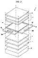
- FIG. 2 is an exploded perspective view illustrating a configuration of the liquid crystal display device shown in FIG. 1 .
- FIG. 3 is an enlarged cross-sectional view illustrating a portion of the liquid crystal display device shown in FIG. 1 .
- FIG. 4 is a plan view illustrating the layout of several pixels of the liquid crystal display device shown in FIG. 1 .
- FIG. 5 is a cross-sectional view taken along the A-A′ line of FIG. 4 .
- FIGS. 6A and 6B are views for explaining the principle of viewing angle compensation.
- FIGS. 7A and 7B are view for explaining the principle of viewing angle compensation.
- FIG. 8 is a view illustrating a laminated configuration of optical components in accordance with a first embodiment of the present invention.
- FIG. 9 is a view illustrating a laminated configuration of optical components in accordance with a second embodiment of the present invention.
- FIG. 10 is a view illustrating a laminated configuration of optical components in accordance with a third embodiment of the present invention.
- FIGS. 11A , 11 B, and 11 C are tables illustrating an axial direction and so forth of each optical component in accordance with the first to third embodiments.
- FIGS. 12A , 12 B, 12 C, and 12 D are graphs illustrating a viewing angle characteristic as compared to the related art.
- FIG. 13 is a perspective view illustrating an example of an electronic apparatus using the liquid crystal display device of the present invention.
- FIG. 1 is a block diagram illustrating an electrical configuration of the liquid crystal display device to which the present invention is applied.
- FIGS. 2 and 3 are an exploded perspective view of the configuration of the liquid crystal display device shown in FIG. 1 , and a partially enlarged cross-sectional view thereof, respectively.
- FIG. 4 is a plan view illustrating the layout of several pixels including a thin film diode (TFD) in the liquid crystal display device, and
- FIG. 5 is a cross-sectional view taken along the line A-A′ of FIG. 4 .
- TFD thin film diode
- the liquid crystal display to which the present invention is applied is an active matrix type transflective liquid crystal display device using nematic liquid crystal, wherein a plurality of scanning lines 31 is arranged in a row direction (x-direction) and a plurality of data lines 21 is arranged in a column direction (y-direction) as shown in FIG. 1 .
- a pixel 11 is formed at each intersection of the scanning line 31 and the data line 21 .
- a liquid crystal layer 12 formed of nematic liquid crystal and a thin film diode (TFD) element 40 as a two-terminal type active element are serially connected to each other in each pixel 11 .
- TDD thin film diode
- the liquid crystal layer 12 is connected to the scanning line 31 , and the TFD element 40 is connected to the data line 21 .
- Each scanning line 31 is driven by the scanning line driving circuit 350
- each data line 21 is driven by the data line driving circuit 250 .
- a driving liquid crystal cell 10 having a pair of transmitting substrates bonded to each other with predetermined spacing is used, while an upper polarizer 2 , at least one upper retardation plate 3 , a driving liquid crystal cell 10 , a plurality of lower retardation plates 5 , a lower polarizer 7 , and a backlight 9 are arranged to overlap each other downward from the upper side in this order.
- the number of the upper retardation plate 3 is different from each other in each embodiment to be described later.
- the transmitting substrate on one side is an element substrate 20 where active elements are formed, and the transmitting substrate on the other side is a counter substrate 30 opposed to the element substrate 20 .
- the element substrate 20 and the counter substrate 30 are bonded by a seal 34 including a spacer (not shown) while maintaining a predetermined gap therebetween, and a liquid crystal layer to be described layer is enclosed within the gap to be retained.
- an integrated circuit (IC) driver for driving the liquid crystal which constitutes the data line driving circuit 250 is directly mounted on a surface of the element substrate 20 by means of a chip on glass (COG) technique, and an IC (driver) for driving the liquid crystal which constitutes the scanning line driving circuit 350 is also directly mounted on a surface of the counter substrate 30 .
- COG chip on glass
- other techniques may be employed to have a connected configuration of the IC chip and the liquid crystal display device instead of the COG technique.
- a tape automated bonding (TAB) technique may be employed to have a tape carrier package (TCP) where an IC chip is bonded on a flexible printed circuit (FPC) to be electrically connected to the liquid crystal display device.
- a technique of bonding the IC chip onto a hard substrate i.e. chip on board (COB)
- COB chip on board
- This pixel electrode 23 is formed of a transparent metal film such as an indium tin oxide (ITO).
- ITO indium tin oxide
- Each data line 21 extends in a straight line, and the TFD element 40 and the pixel electrode 23 are arranged in a dot matrix.
- An alignment film 24 is formed on the surface of the pixel electrode 23 which has been subjected to a rubbing process as one axial alignment process having conditions to be described later.
- This alignment film 24 is generally formed of a polyimide resin or the like.
- a layer-thickness adjusting film for adjusting the thickness of the liquid crystal layer 12 in the transmissive display region 14 and the thickness of the liquid crystal layer 12 in the reflective display region 13 a partially reflecting layer 33 formed of a single layer or a multi-layer made of aluminum, aluminum alloy, silver, silver alloy, etc. or laminated layers thereof, a color filter 34 , an overcoat layer 35 , a belt-shaped counter electrode 36 formed of a transparent metal film such as ITO or the like, and an alignment film 37 are formed on an inner surface of the counter substrate 30 .
- the layer-thickness adjusting film 32 and the partially reflecting layer 33 are selectively formed in the reflective display region 13 of the pixel 11 , and are not formed in the transmissive display region 14 .
- the color filter 34 has three colored layers of red (R), green (G), and blue (B) colors.
- a black matrix 38 is formed in a gap between each colored layer, and is configured to block lights incident from the gaps of the colored layers.
- the overcoat layer 35 is formed for the purpose of increasing the smoothness of the black matrix 38 and the color filter 34 in the surface of the black matrix 38 and the color filter 34 to thereby prevent disconnection of the counter electrode 36 .
- the counter electrode 36 functions as a scanning line 31 , and is formed in a direction orthogonal to the data line 21 .
- the alignment film 37 which has been subjected to a rubbing process such as one axial rubbing process is formed in the surface of the counter electrode 36 using conditions to be described later.
- This alignment film 37 is generally formed of polyimide resin or the like.
- the TFD element 40 has a first TFD element 40 a and a second TFD element 40 b , and is formed of a first metal film 42 , an oxide film 44 as an insulator formed by anodization on the surface of the first metal film 42 , and second metal films 46 a and 46 b formed on the surface and spaced from each other.
- the second metal film 46 a functions as the data line 21 while the second metal film 46 b is connected to the pixel electrode 23 formed of an ITO film or the like.
- the first TFD element 40 a is formed of the second metal film 46 a , the oxide film 44 , and the first metal film 42 in the order as seen from the side of data line 21 , and has a sandwiched structure of:
- the TFD element 40 is one example of the diode element, and a zinc oxide (ZnO) varistor, an element using a metal semi-insulator (MSI) or the like, a single body thereof, a serial connection thereof in a reverse direction, or a parallel connection thereof in a reverse direction may also be employed for the same.
- ZnO zinc oxide
- MSI metal semi-insulator
- the layer-thickness adjusting film 32 is configured so as to meet the relationship as follows: dh ⁇ dt, wherein dh denotes the thickness of the liquid crystal layer 12 (nematic liquid crystal layer) corresponding to the reflective display region 13 , and dt denotes the thickness of the liquid crystal layer 12 corresponding to the transmissive display region 14 .
- the thickness dh of the liquid crystal layer 12 of the reflective display region 13 is set to 3.0 ⁇ m
- the thickness dt of the liquid crystal layer 12 corresponding to the transmissive display region 14 is set to 5.0 ⁇ m. Accordingly, when the birefringence of the liquid crystal molecule is 0.05, the retardation value ⁇ nd of the reflective display region 13 is 150 nm while the retardation value ⁇ nd of the transmissive display region 14 is 250 nm.
- liquid crystal display device 1 when the reflective display is performed, external light incident from the outside of the device (i.e. the element substrate 20 ) are used, which are incident on the liquid crystal layer 12 from the element substrate 20 and reflected by the partially reflecting layer 33 (reflective display region 13 ), which are then transmitted again through the liquid crystal layer 12 and exited from the element substrate 20 , thereby performing the color display in the reflecting mode.
- the liquid crystal of the liquid crystal layer 12 between the pixel electrode 23 and the counter electrode 36 is controlled in its alignment, so that the bright and dark display is performed.
- the transmissive display in order to perform the transmissive display, light emitted from the backlight 9 are transmitted through the transmissive display region 14 from the counter substrate 30 to be incident on the liquid crystal layer 12 , which are exited from the element substrate 20 , so that the color display is performed in the transmitting mode.
- the liquid crystal of the liquid crystal layer 12 between the pixel electrode 23 and the counter electrode 36 is also controlled in its alignment, so that the bright and dark display is performed.
- the incident light is transmitted through the liquid crystal layer 12 two times, while the transmitted light emitted from the backlight 9 is transmitted through the liquid crystal layer 12 only one time. Therefore, in consideration of the retardation of the liquid crystal layer 12 , this retardation of the liquid crystal layer causes a difference in transmittance of the liquid crystal.
- a predetermined magnitude relation is given to the thickness dh of the liquid crystal layer 12 corresponding to the reflective display region 13 and the thickness dt of the liquid crystal layer 12 corresponding to the transmissive display region 14 , so that a retardation value ⁇ nd in the reflective display region 13 is set to be higher than the retardation value ⁇ nd in the transmissive display region 14 .
- a layer-thickness adjusting layer 35 formed of a photosensitive resin is selectively formed on an inner surface of the counter substrate 30 , however, it is also possible to selectively etch the surface of the counter substrate 30 to form a concave portion, and to adjust the thickness of the liquid crystal layer 12 in the reflective display region 13 and the thickness of the liquid crystal layer 12 in the transmissive display region 14 by means of the concave portion.
- the liquid crystal molecule 50 of the nematic liquid crystal has a birefringence property, so that the refractive index of the axial direction (x direction) of the liquid crystal molecule 50 is different from that vertical to the direction (y direction). Accordingly, the optical path length of light is different from each other depending on the observation direction of the observer, which leads to a difference in contrast or brightness (that is, the viewing angle dependency is said to be high). This is the fundamental reason why the viewing angle is decreased.
- a viewing angle compensation film is used in a pseudo manner in the present invention to thereby make the refractive index characteristic closer to that of the sphere shown in FIG. 6B . That is, a liquid crystal film and a polymer film are laminated with respect to the liquid crystal layer 12 of the liquid crystal display device 1 , so that the refractive index characteristic of the whole laminate is made closer to that of the sphere in a three-dimensional manner.
- a liquid crystal film 54 aligned in a discotic hybrid manner is first used to compensate for the tilt of the liquid crystal layer 12 of the liquid crystal display device 1 as shown in FIG. 7A . That is, the tilt of the liquid crystal layer 12 is compensated by the discotic liquid crystal constituting the liquid crystal film 54 as shown in FIG. 7B .
- the tilt direction of the nematic liquid crystal within the liquid crystal layer 12 is made to cross the tilt direction of the discotic liquid crystal within the liquid crystal film 54 , so that the tilt of the liquid crystal layer 12 is compensated.
- the tilt of the liquid crystal layer 12 is compensated by the liquid crystal 54 and the phase difference is generated in the z-axis direction by the polymer film 59 , so that the refractive index may be made closer to that of the sphere by the laminate of the liquid crystal 12 , the liquid crystal film 54 , and the polymer film 59 in a pseudo manner, which allows the viewing angle dependency to be suppressed.
- FIG. 8 is a view for explaining an axial direction and so forth of each optical component used for the liquid crystal display device to which the present invention is applied.
- an upper polarizer 2 upper retardation plates 3 a and 3 c , a driving liquid crystal cell 10 , lower retardation plates 5 a to 5 c , a lower polarizer 7 , and a backlight 9 are arranged to overlap each other in this order downward from the upper side as shown in FIGS. 2 and 8 .
- a low dispersion film is used for the upper retardation plates 3 a and 3 b and the lower retardation plate 5 c .
- a discotic liquid crystal film as the above-described liquid crystal film 54 is used for the lower retardation plate 5 a .
- a polymer film having a three-dimensional refractive index anisotropy as the above-described polymer film 59 is used for the lower retardation plate 5 b.
- FIG. 11A The axial angle of each member shown in FIG. 8 and a phase difference value obtained by the axial angle are shown in FIG. 11A .
- rubbing is performed on the nematic liquid crystal layer 12 in a direction in which a predetermined angle is formed with respect to the three o'clock direction shown as a broken line with respect to the element substrate 20 and the counter substrate 30 , so that the twist angle ⁇ LC is set to 0° to 70°.
- the rubbing direction of the element substrate 20 (upper substrate) of the liquid crystal cell 10 is set to an angle ⁇ Lcu in a counterclockwise direction from the reference direction
- the rubbing direction of the counter substrate 30 (lower substrate) is set to an angle ⁇ Lcd in a counterclockwise direction from the reference direction.
- the angle ⁇ Lcu is in a preferable range of 80° to 130°, and particularly preferably about 90°
- the angle ⁇ Lcd is in a preferable range of 230° to 270°, and particularly preferably about 270°.
- the polarizer 2 where the absorbing axis 201 has an angle ⁇ pu with respect to the reference direction as seen from the top, is employed.
- the angle ⁇ pu is in a preferable range of ⁇ 80° to 80°, and particularly preferably about 15°.
- the angle ⁇ F 1 is in a preferable range of ⁇ 60° to 60°, and particularly preferably about 30°.
- the phase difference RF 3 a due to the lower retardation plate 3 a is in a preferable range of 220 nm to 290 nm, and particularly preferably about 260 nm.
- the low dispersion film has a lower refractive index when the measured wavelength becomes shorter.
- the same configuration is applied to the upper retardation plate 3 b and the lower retardation plate 5 c.
- the angle ⁇ F 2 is in a preferable range of 45° to 135°, and particularly preferably about 90°.
- the phase difference RF 3 b due to the lower retardation plate 3 b is in a preferable range of 50 nm to 140 nm, and particularly preferably about 90 nm.
- a discotic liquid crystal film with hybrid alignment where a hybrid alignment axis 501 a has an angle ⁇ F 3 with respect to the reference direction is used as the lower retardation plate 5 a .
- the angle ⁇ F 3 is in a preferable range of 85° to 95°, and particularly preferably about 90°.
- the phase difference RF 5 a due to the lower retardation plate 5 a is in a preferable range of 10 nm to 40 nm, and particularly preferably about 26 nm.
- a polymer film where the phase retardation axis 501 b has an angle ⁇ F 4 with respect to the reference direction is used as the lower retardation plate 5 b .
- the angle ⁇ F 4 is in a preferable range of 85° to 95°, and particularly preferably about 90°.
- the phase difference RF 5 b due to the lower retardation plate 5 b is in a preferable range of 80 nm to 150 nm, and particularly preferably about 130 nm.
- a low dispersion film where the phase retardation axis 501 c has an angle ⁇ F 5 with respect to the reference direction is used as the lower retardation plate 5 c .
- the phase difference RF 5 c due to the lower retardation plate 5 c is in a preferable range of 220 nm to 290 nm, and particularly preferably about 270 nm.
- the lower polarizer 7 is preferably used wherein the absorbing axis 701 has an angle ⁇ pd with respect to the reference direction.
- the angle ⁇ pd is in a preferable range of 45° to 135°, and particularly preferably about 75°.
- the viewing angle characteristic was improved two times or more in the transmitting mode when the display performance was measured with respect to the liquid crystal display device 1 having the above-mentioned configuration.
- the color variation due to the viewing angle was reduced, which allowed the contrast to be increased two times or more.
- FIG. 9 is a view for explaining an axial direction or the like of each optical component using a liquid crystal display device according to the second embodiment.
- an upper polarizer 2 In order to fabricate the liquid crystal display device 1 using the driving liquid crystal cell 10 of the present embodiment, an upper polarizer 2 , an upper retardation plate 3 c , a driving liquid crystal cell 10 , lower retardation plates 5 a to 5 c , a lower polarizer 7 , and a backlight 9 are arranged to overlap each other in this order downward from the upper side as shown in FIG. 9 .
- the upper retardation plate 3 c is used in the second embodiment instead of the upper retardation plates 3 a and 3 b in the first embodiment.
- the other configuration is same as that of the first embodiment. That is, the configuration of the upper polarizer 2 , the liquid crystal 10 , the lower retardation plates 5 a to 5 c , and the lower polarizer 7 is same as that of the first embodiment, so that its description will be skipped.
- the axial angle of each member shown in FIG. 9 and a phase difference value obtained therefrom are shown in FIG. 11B .
- a retardation plate of a reverse wavelength diffusion type which shows a lower phase difference value in the shorter wavelength in a measurement wavelength range of 400 nm to 700 nm, is used as the upper retardation plate 3 c in the second embodiment.
- the upper retardation plate may be configured with one sheet.
- the angle ⁇ F 6 is in a preferable range of ⁇ 60° to 60°, and particularly preferably about 50°.
- the phase difference RF 3 c due to the upper retardation plate 3 c is in a preferable range of 100 nm to 200 nm, and particularly preferably about 170 nm.
- the lower retardation plate 5 a to 5 c and the lower polarizer 7 which are disposed below the liquid crystal cell 10 are same as that of the first embodiment, so that the same effect of improving the viewing angle is obtained as the first embodiment.
- a reverse wavelength diffusion film is used in the second embodiment to allow one sheet of the upper retardation plate to be employed, which may lead to the thin liquid crystal display device 1 by its reduced thickness.
- FIG. 10 is a view for explaining an axial direction or the like of each optical component using a liquid crystal display device according to the third embodiment.
- an upper polarizer 2 In order to fabricate the liquid crystal display device 1 using the driving liquid crystal cell 10 of the present embodiment, an upper polarizer 2 , upper retardation plates 3 d to 3 f , a driving liquid crystal cell 10 , lower retardation plates 5 a to 5 c , a lower polarizer 7 , and a backlight 9 are arranged to overlap each other in this order downward from the upper side as shown in FIG. 10 .
- the upper retardation plates 3 d to 3 f are used in the third embodiment instead of the upper retardation plates 3 a and 3 b in the first embodiment.
- the other configuration is same as that of the first embodiment. That is, the configuration of the upper polarizer 2 , the liquid crystal 10 , the lower retardation plates 5 a to 5 c , and the lower polarizer 7 is same as that of the first embodiment, so that its description will be skipped.
- the axial angle of each member shown in FIG. 10 and a phase difference value obtained therefrom are shown in FIG. 11C .
- a configuration improving the viewing angle by using a discotic liquid crystal film with hybrid alignment and a polymer film having a three-dimensional refractive index anisotropy, namely, the same configuration as that of the lower retardation plates 5 a to 5 c is also employed for upper retardation plates.
- the laminating order is symmetric with the liquid crystal cell 10 being a reference.
- the upper retardation plate 3 f uses a discotic liquid crystal film with hybrid alignment which is same as that of the lower retardation plate 5 a
- the upper retardation plate 3 e uses a polymer film having a three-dimensional refractive index anisotropy which is same as that of the lower retardation plate 5 b
- the upper retardation plate 3 d uses a low dispersion film which is same as that of the upper retardation plate 3 d.
- a low dispersion film wherein the phase retardation axis 301 d has an angle ⁇ F 7 with respect to the reference direction is used as the upper retardation plate 3 d .
- the angle ⁇ F 7 is in a preferable range of ⁇ 60′ to 60°, and particularly preferably about 30°.
- the phase difference RF 3 d due to the upper retardation plate 3 d is in a preferable range of 220 nm to 290 nm, and particularly preferably about 265 nm.
- a polymer film having the three-dimensional refractive index anisotropy is used as the upper retardation plate 3 e wherein the phase retardation axis 301 e has an angle ⁇ F 8 with respect to the reference direction.
- the angle ⁇ F 8 is in a preferable range of 45° to 135°, and particularly preferably about 90°.
- the phase difference RF 3 e due to the upper retardation plate 3 e is in a preferable range of 50 nm to 140 nm, and particularly preferably about 130 nm.
- a discotic liquid crystal film with hybrid alignment is used as the upper retardation plate 3 f wherein the hybrid alignment axis 301 f has an angle ⁇ F 9 with respect to the reference direction.
- the angle ⁇ F 9 is in a preferable range of 45° to 135°, and particularly preferably about 90°.
- the phase difference RF 3 f due to the upper retardation plate 3 f is in a preferable range of 10 nm to 40 nm, and particularly preferably about 30 nm.
- a combination of the discotic liquid crystal film with hybrid alignment and a polymer film having a three-dimensional refractive index anisotropy is provided in both of the upper and lower positions of the liquid crystal cell 10 , so that the viewing angle characteristic may be further improved in the transmitting mode. Specifically, it was found that the viewing angle characteristic was improved two and a half times or more in the transmitting mode when the display performance was measured with respect to the liquid crystal display device 1 having the above-mentioned configuration. In addition, the color variation due to the viewing angle was reduced, which allowed the contrast to be increased two times or more.
- FIG. 12 shows the viewing angle characteristics of the configuration according to the above-mentioned embodiment and the conventional configuration.
- FIG. 12A shows the viewing angle characteristic of the liquid crystal display device 1 according to the first embodiment.
- FIG. 12B shows the viewing angle characteristic of the liquid crystal display device using the optical compensation film substantially formed of a liquid crystalline polymer representing a positive one axial property optically wherein the liquid crystalline polymer has fixed the nematic hybrid alignment formed in the liquid crystal state.
- a circle graph representing the viewing angle characteristic has an azimuth angle ⁇ in a circumferential direction and an elevation angle ⁇ in a radial direction.
- the azimuth angle ⁇ indicates the angle of deviation in up, down, left and right directions of an observer as shown in FIG. 12C .
- the elevation angle ⁇ indicates an angle where the line of sight of the observer is formed with respect to the normal line NL of the liquid crystal display device 1 as shown in FIG.
- the length of the circle in the radial direction indicates the elevation angle ⁇ .
- concentric circles denoted by broken lines in the circle graph of FIG. 12A indicate elevation angles corresponding to 20°, 40°, 60°, and 80° from an inner circumferential side of the broken line.
- a white area has a contrast not less than 10
- a black area has a contrast less than 10.
- the contrast of 10 often becomes a reference for determining the visibility as a good state, and the circle graphs shown in FIGS. 12A and 12B are also classified into the white area and the black area by color with the contrast of 10 being a boundary thereof.
- the white area spreads toward the outer circumferential side of the circle in the viewing angle characteristic of the liquid crystal display device 1 of the first embodiment shown in FIG. 12A as compared to the viewing angle characteristic of the conventional configuration shown in FIG. 12B . That is, it can be understood that the viewing angle is improved in all directions. Specifically, the contrast becomes 10 or more till the elevation angle of about 40° in almost all directions in the viewing angle characteristic of the conventional configuration shown in FIG. 12B , whereas the contrast is degraded to less than 10 when the elevation angle exceeds 40°. On the contrary, the azimuth is increased which maintains the contrast not less than 10 till the elevation angle of about 50° in the viewing angle characteristic of the first embodiment shown in FIG. 12A . As such, the viewing angle is improved in all directions according to the liquid crystal display device of the present embodiments.
- FIG. 12 shows only the viewing angle characteristic of the liquid crystal display device 1 according to the first embodiment, however, the viewing angle is also improved in the liquid crystal display device according to the second and third embodiments.
- the TFD element 40 is used as the active element in the above-mentioned embodiments, the present invention may also be applied to the liquid crystal display device using a thin film transistor (TFT) instead of the TFD.
- TFT thin film transistor
- the liquid crystal is twisted by the alignment film which has been rubbed in the above-mentioned embodiment, however, the liquid crystal may be twisted by other method.
- the alignment film may be fabricated depositing a silicon oxide or the like on the surface of the substrate obliquely.
- the intensity of light may be adjusted in a stripe to use the photo-curable resin layer which has been exposed and cured as an alignment film.
- FIG. 13 is a perspective view illustrating a configuration of a portable telephone as an example of an electronic apparatus to which the liquid crystal display device 1 of the present invention is mounted.
- a portable telephone 1400 has an earpiece 1404 , a mouthpiece 1406 , and a liquid crystal display 1 as well as a plurality of operation buttons 1402 .
- a backlight is also mounted on the back of the liquid crystal display 1 if necessary.
- a mobile computer In addition to the portable telephone, a mobile computer, a liquid crystal television, a view finder type or monitor direct-view type video tape recorder, a car navigation apparatus, an electronic note, an electronic calculator, a word processor, a workstation, a picture phone, a point-of-sale (POS) terminal, or an apparatus having a touch panel may employed as the electronic apparatus which may mount the liquid crystal display device of the present embodiment.
- a mobile computer a liquid crystal television, a view finder type or monitor direct-view type video tape recorder, a car navigation apparatus, an electronic note, an electronic calculator, a word processor, a workstation, a picture phone, a point-of-sale (POS) terminal, or an apparatus having a touch panel may employed as the electronic apparatus which may mount the liquid crystal display device of the present embodiment.
- POS point-of-sale
Landscapes
- Physics & Mathematics (AREA)
- Nonlinear Science (AREA)
- General Physics & Mathematics (AREA)
- Mathematical Physics (AREA)
- Chemical & Material Sciences (AREA)
- Crystallography & Structural Chemistry (AREA)
- Optics & Photonics (AREA)
- Liquid Crystal (AREA)
- Structural Engineering (AREA)
- Civil Engineering (AREA)
- Architecture (AREA)
- Engineering & Computer Science (AREA)
- Polarising Elements (AREA)
Abstract
Description
-
- metal(conductor)/insulator/metal(conductor),
- so that it has a bi-directional diode switching characteristic of positive and negative polarities. In the meantime, the
second TFD element 40 b is formed of thefirst metal film 42, theoxide film 44, and thesecond metal film 46 b in the order as seen from the side ofdata line 21, and has a diode switching characteristic opposite to that of thefirst TFD element 40 a. Accordingly, theTFD element 40 has a symmetrically nonlinear characteristic of current-voltage in the positive and negative polarities as compared to the case of using one diode. Alternatively, when such a nonlinear characteristic is not strictly required to be symmetrical, only oneTFD element 40 may be employed.
Claims (9)
Applications Claiming Priority (4)
| Application Number | Priority Date | Filing Date | Title |
|---|---|---|---|
| JP2004-051667 | 2004-02-26 | ||
| JP2004051667 | 2004-02-26 | ||
| JP2004324748A JP4046116B2 (en) | 2004-02-26 | 2004-11-09 | Liquid crystal device and electronic device |
| JP2004-324748 | 2004-11-09 |
Publications (2)
| Publication Number | Publication Date |
|---|---|
| US20050190328A1 US20050190328A1 (en) | 2005-09-01 |
| US7583343B2 true US7583343B2 (en) | 2009-09-01 |
Family
ID=34889392
Family Applications (1)
| Application Number | Title | Priority Date | Filing Date |
|---|---|---|---|
| US11/065,749 Active 2026-09-02 US7583343B2 (en) | 2004-02-26 | 2005-02-25 | Liquid crystal display device and electronic apparatus |
Country Status (4)
| Country | Link |
|---|---|
| US (1) | US7583343B2 (en) |
| JP (1) | JP4046116B2 (en) |
| KR (1) | KR100639444B1 (en) |
| CN (1) | CN100367092C (en) |
Families Citing this family (10)
| Publication number | Priority date | Publication date | Assignee | Title |
|---|---|---|---|---|
| JP4788111B2 (en) * | 2004-05-27 | 2011-10-05 | セイコーエプソン株式会社 | Liquid crystal device and electronic device |
| KR100762028B1 (en) * | 2005-10-14 | 2007-09-28 | 비오이 하이디스 테크놀로지 주식회사 | Transflective Liquid Crystal Display with High Transmittance and Wide Viewing Angle |
| US7616278B2 (en) * | 2005-12-05 | 2009-11-10 | Tpo Displays Corp. | Liquid crystal displays |
| JP5072520B2 (en) * | 2006-12-19 | 2012-11-14 | 株式会社ジャパンディスプレイセントラル | Liquid crystal display |
| US7589811B2 (en) | 2006-12-19 | 2009-09-15 | Toshiba Matsushita Display Technology Co., Ltd. | Liquid crystal display device |
| JP5104110B2 (en) * | 2007-05-30 | 2012-12-19 | 日本ゼオン株式会社 | Polarizing plate and liquid crystal display device |
| KR101129546B1 (en) * | 2008-03-07 | 2012-03-29 | 삼성코닝정밀소재 주식회사 | Filter for display apparatus |
| CN101614911B (en) * | 2008-06-27 | 2011-07-27 | 群康科技(深圳)有限公司 | LCD panel |
| JP5027086B2 (en) * | 2008-09-25 | 2012-09-19 | 株式会社ジャパンディスプレイウェスト | Input device and display device with input function |
| CN102650760A (en) * | 2011-02-25 | 2012-08-29 | 瀚宇彩晶股份有限公司 | Liquid crystal display panel and liquid crystal display device |
Citations (20)
| Publication number | Priority date | Publication date | Assignee | Title |
|---|---|---|---|---|
| CN1053302A (en) | 1989-12-08 | 1991-07-24 | 精工爱普生株式会社 | Liquid crystal indicator |
| JPH05100114A (en) | 1991-10-07 | 1993-04-23 | Nitto Denko Corp | Laminated wavelength plate and circularly polarizing plate |
| JPH09203895A (en) | 1995-08-17 | 1997-08-05 | Toshiba Corp | Liquid crystal display element and optically anisotropic element |
| JPH1033314A (en) | 1996-07-29 | 1998-02-10 | Kansai Seisakusho:Kk | Lift controller for electric rising and descending bed |
| JPH10186356A (en) | 1996-12-27 | 1998-07-14 | Nippon Oil Co Ltd | Optical compensation film for liquid crystal display devices |
| JPH10206637A (en) | 1997-01-17 | 1998-08-07 | Nippon Oil Co Ltd | Optical element film |
| CN1281157A (en) | 1999-06-30 | 2001-01-24 | 卡西欧计算机株式会社 | Liquid crystal display with wide angle of field |
| US20010030726A1 (en) * | 2000-04-06 | 2001-10-18 | Fujitsu Limited | Viewing angle compensation film and liquid crystal display |
| US6411355B1 (en) * | 1995-08-17 | 2002-06-25 | Toshiba Techno Center Inc. | Liquid crystal display device with compensation for viewing angle dependency and optical anisotropic element used therein |
| CN1392964A (en) | 2000-09-27 | 2003-01-22 | 松下电器产业株式会社 | Transreflective liquid crystal display |
| JP2003090914A (en) | 2001-09-18 | 2003-03-28 | Teijin Ltd | Retardation film and method for producing the same |
| WO2003085949A2 (en) | 2002-04-04 | 2003-10-16 | Samsung Electronics Co., Ltd. | Liquid crystal display provided with compensation film |
| JP2003322855A (en) | 2002-05-01 | 2003-11-14 | Toshiba Corp | Liquid crystal display device |
| US6801283B2 (en) * | 2002-05-10 | 2004-10-05 | Advanced Display Inc. | Liquid crystal display device |
| US6816217B2 (en) * | 2002-01-25 | 2004-11-09 | Alps Electric Co., Ltd. | Transflective liquid-crystal display device |
| US20040233362A1 (en) * | 2002-09-06 | 2004-11-25 | Dai Nippon Prtg. Co., Ltd. | Laminated retardation optical element, process of producing the same, and liquid crystal display |
| US20050041180A1 (en) * | 2003-02-06 | 2005-02-24 | Seiko Epson Corporation | Liquid crystal display device and electronic apparatus |
| US20050087704A1 (en) | 2000-04-25 | 2005-04-28 | Mitsubishi Heavy Industries Ltd. | Radioactive substance container, manufacturing apparatus thereof and manufacturing method thereof |
| US20060072054A1 (en) * | 2002-12-13 | 2006-04-06 | Fuji Photo Film Co., Ltd. | Liquid crystal display of ocb or va mode |
| US20060114385A1 (en) * | 2003-10-29 | 2006-06-01 | Fuji Photo Film Co., Ltd. | Liquid crystal display having liquid crystal cell of bend alignment mode or hybrid alignment mode |
Family Cites Families (4)
| Publication number | Priority date | Publication date | Assignee | Title |
|---|---|---|---|---|
| WO1996031793A1 (en) * | 1995-04-07 | 1996-10-10 | Nippon Oil Company, Limited | Liquid-crystalline optical film and its utilization |
| JP2001249334A (en) * | 2000-03-06 | 2001-09-14 | Hitachi Ltd | Liquid crystal display device |
| JP2002148434A (en) * | 2000-11-08 | 2002-05-22 | Nitto Denko Corp | Polarizer |
| EP1341007A4 (en) * | 2000-12-04 | 2011-03-23 | Fujifilm Corp | Optical compensating sheet having optically anisotropic layer made of discotic liquid-crystalline molecules and transparent substrate comprising polymer film |
-
2004
- 2004-11-09 JP JP2004324748A patent/JP4046116B2/en not_active Expired - Lifetime
-
2005
- 2005-02-24 KR KR1020050015231A patent/KR100639444B1/en not_active Expired - Lifetime
- 2005-02-25 CN CNB2005100510471A patent/CN100367092C/en not_active Expired - Lifetime
- 2005-02-25 US US11/065,749 patent/US7583343B2/en active Active
Patent Citations (25)
| Publication number | Priority date | Publication date | Assignee | Title |
|---|---|---|---|---|
| US5139340A (en) | 1989-12-08 | 1992-08-18 | Seiko Epson Corporation | Single polarizer, reflective type liquid crystal display device with high brightness and contrast ratio |
| CN1053302A (en) | 1989-12-08 | 1991-07-24 | 精工爱普生株式会社 | Liquid crystal indicator |
| JPH05100114A (en) | 1991-10-07 | 1993-04-23 | Nitto Denko Corp | Laminated wavelength plate and circularly polarizing plate |
| US6411355B1 (en) * | 1995-08-17 | 2002-06-25 | Toshiba Techno Center Inc. | Liquid crystal display device with compensation for viewing angle dependency and optical anisotropic element used therein |
| JPH09203895A (en) | 1995-08-17 | 1997-08-05 | Toshiba Corp | Liquid crystal display element and optically anisotropic element |
| JPH1033314A (en) | 1996-07-29 | 1998-02-10 | Kansai Seisakusho:Kk | Lift controller for electric rising and descending bed |
| JPH10186356A (en) | 1996-12-27 | 1998-07-14 | Nippon Oil Co Ltd | Optical compensation film for liquid crystal display devices |
| JPH10206637A (en) | 1997-01-17 | 1998-08-07 | Nippon Oil Co Ltd | Optical element film |
| US6307608B1 (en) | 1999-06-30 | 2001-10-23 | Casio Computer Co., Ltd. | Liquid crystal display having wide viewing angle range |
| CN1281157A (en) | 1999-06-30 | 2001-01-24 | 卡西欧计算机株式会社 | Liquid crystal display with wide angle of field |
| US20010030726A1 (en) * | 2000-04-06 | 2001-10-18 | Fujitsu Limited | Viewing angle compensation film and liquid crystal display |
| JP2002182036A (en) | 2000-04-06 | 2002-06-26 | Fujitsu Ltd | Viewing angle compensation film and liquid crystal display device |
| US20050087704A1 (en) | 2000-04-25 | 2005-04-28 | Mitsubishi Heavy Industries Ltd. | Radioactive substance container, manufacturing apparatus thereof and manufacturing method thereof |
| CN1392964A (en) | 2000-09-27 | 2003-01-22 | 松下电器产业株式会社 | Transreflective liquid crystal display |
| US6771334B2 (en) | 2000-09-27 | 2004-08-03 | Matsushita Electric Industrial Co., Ltd. | Transflective liquid crystal display device |
| JP2003090914A (en) | 2001-09-18 | 2003-03-28 | Teijin Ltd | Retardation film and method for producing the same |
| US6816217B2 (en) * | 2002-01-25 | 2004-11-09 | Alps Electric Co., Ltd. | Transflective liquid-crystal display device |
| WO2003085949A2 (en) | 2002-04-04 | 2003-10-16 | Samsung Electronics Co., Ltd. | Liquid crystal display provided with compensation film |
| JP2003322855A (en) | 2002-05-01 | 2003-11-14 | Toshiba Corp | Liquid crystal display device |
| US20050057704A1 (en) * | 2002-05-01 | 2005-03-17 | Toshiya Ootake | Liquid crystal display device |
| US6801283B2 (en) * | 2002-05-10 | 2004-10-05 | Advanced Display Inc. | Liquid crystal display device |
| US20040233362A1 (en) * | 2002-09-06 | 2004-11-25 | Dai Nippon Prtg. Co., Ltd. | Laminated retardation optical element, process of producing the same, and liquid crystal display |
| US20060072054A1 (en) * | 2002-12-13 | 2006-04-06 | Fuji Photo Film Co., Ltd. | Liquid crystal display of ocb or va mode |
| US20050041180A1 (en) * | 2003-02-06 | 2005-02-24 | Seiko Epson Corporation | Liquid crystal display device and electronic apparatus |
| US20060114385A1 (en) * | 2003-10-29 | 2006-06-01 | Fuji Photo Film Co., Ltd. | Liquid crystal display having liquid crystal cell of bend alignment mode or hybrid alignment mode |
Non-Patent Citations (1)
| Title |
|---|
| Communication from Japanese Patent Office regarding related application. |
Also Published As
| Publication number | Publication date |
|---|---|
| JP2005275359A (en) | 2005-10-06 |
| CN100367092C (en) | 2008-02-06 |
| CN1661442A (en) | 2005-08-31 |
| US20050190328A1 (en) | 2005-09-01 |
| KR100639444B1 (en) | 2006-10-26 |
| KR20060043168A (en) | 2006-05-15 |
| JP4046116B2 (en) | 2008-02-13 |
Similar Documents
| Publication | Publication Date | Title |
|---|---|---|
| US7705933B2 (en) | Liquid crystal display apparatus and electronic apparatus | |
| US8520173B2 (en) | Display device | |
| KR100816145B1 (en) | Liquid crystal device and electronic apparatus | |
| JP3692445B2 (en) | Liquid crystal device and electronic device | |
| US8625063B2 (en) | Display and electronic unit having particular optical laminate | |
| US8319922B2 (en) | Liquid crystal display and electronic apparatus | |
| KR20080110541A (en) | Liquid Crystal Devices and Electronic Devices | |
| US7830481B2 (en) | Liquid crystal display device with retardations of optical films and liquid crystal layer | |
| US7583343B2 (en) | Liquid crystal display device and electronic apparatus | |
| JP3901172B2 (en) | Liquid crystal display device and electronic device | |
| JP2004240177A (en) | Liquid crystal display and electronic equipment | |
| JP4813550B2 (en) | Display device | |
| JP4449335B2 (en) | Liquid crystal display device and electronic device | |
| KR20000048388A (en) | Liquid crystal device and electronic equipment using the same | |
| JP4788111B2 (en) | Liquid crystal device and electronic device | |
| JP4254092B2 (en) | Liquid crystal display panel and electronic equipment | |
| JP2004280077A (en) | Liquid crystal device and electronic equipment using the same | |
| JP2006098467A (en) | Liquid crystal device and electronic device | |
| JP2007334085A (en) | Liquid crystal display device, and electronic apparatus | |
| US8742416B2 (en) | Display panel, method of manufacturing display panel, display device, and electronic apparatus | |
| JP4858082B2 (en) | Electro-optical device and electronic apparatus | |
| JP4923947B2 (en) | Electro-optical device and electronic apparatus | |
| JP4042758B2 (en) | Liquid crystal device and electronic device | |
| JP2005114982A (en) | Liquid crystal device and electronic device | |
| JP2005114983A (en) | Liquid crystal device and electronic device |
Legal Events
| Date | Code | Title | Description |
|---|---|---|---|
| AS | Assignment |
Owner name: SEIKO EPSON CORPORATION, JAPAN Free format text: ASSIGNMENT OF ASSIGNORS INTEREST;ASSIGNOR:SEKIME, TOMOAKI;REEL/FRAME:016338/0845 Effective date: 20050125 |
|
| STCF | Information on status: patent grant |
Free format text: PATENTED CASE |
|
| FEPP | Fee payment procedure |
Free format text: PAYOR NUMBER ASSIGNED (ORIGINAL EVENT CODE: ASPN); ENTITY STATUS OF PATENT OWNER: LARGE ENTITY |
|
| FPAY | Fee payment |
Year of fee payment: 4 |
|
| AS | Assignment |
Owner name: BOE TECHNOLOGY (HK) LIMITED, CHINA Free format text: ASSIGNMENT OF ASSIGNORS INTEREST;ASSIGNOR:SEIKO EPSON CORPORATION;REEL/FRAME:037515/0050 Effective date: 20141118 Owner name: BOE TECHNOLOGY GROUP CO., LTD., CHINA Free format text: ASSIGNMENT OF ASSIGNORS INTEREST;ASSIGNOR:BOE TECHNOLOGY (HK) LIMITED;REEL/FRAME:037515/0082 Effective date: 20150214 |
|
| FPAY | Fee payment |
Year of fee payment: 8 |
|
| MAFP | Maintenance fee payment |
Free format text: PAYMENT OF MAINTENANCE FEE, 12TH YEAR, LARGE ENTITY (ORIGINAL EVENT CODE: M1553); ENTITY STATUS OF PATENT OWNER: LARGE ENTITY Year of fee payment: 12 |