US7581314B2 - Method of forming noble metal contacts - Google Patents
Method of forming noble metal contacts Download PDFInfo
- Publication number
- US7581314B2 US7581314B2 US11/358,823 US35882306A US7581314B2 US 7581314 B2 US7581314 B2 US 7581314B2 US 35882306 A US35882306 A US 35882306A US 7581314 B2 US7581314 B2 US 7581314B2
- Authority
- US
- United States
- Prior art keywords
- dielectric layer
- contact
- metal
- noble metal
- layer
- Prior art date
- Legal status (The legal status is an assumption and is not a legal conclusion. Google has not performed a legal analysis and makes no representation as to the accuracy of the status listed.)
- Expired - Fee Related, expires
Links
Images


Classifications
-
- H—ELECTRICITY
- H01—ELECTRIC ELEMENTS
- H01H—ELECTRIC SWITCHES; RELAYS; SELECTORS; EMERGENCY PROTECTIVE DEVICES
- H01H59/00—Electrostatic relays; Electro-adhesion relays
- H01H59/0009—Electrostatic relays; Electro-adhesion relays making use of micromechanics
-
- H—ELECTRICITY
- H01—ELECTRIC ELEMENTS
- H01H—ELECTRIC SWITCHES; RELAYS; SELECTORS; EMERGENCY PROTECTIVE DEVICES
- H01H1/00—Contacts
- H01H1/02—Contacts characterised by the material thereof
- H01H1/021—Composite material
- H01H1/023—Composite material having a noble metal as the basic material
-
- H—ELECTRICITY
- H01—ELECTRIC ELEMENTS
- H01H—ELECTRIC SWITCHES; RELAYS; SELECTORS; EMERGENCY PROTECTIVE DEVICES
- H01H1/00—Contacts
- H01H1/0036—Switches making use of microelectromechanical systems [MEMS]
- H01H2001/0052—Special contact materials used for MEMS
-
- Y—GENERAL TAGGING OF NEW TECHNOLOGICAL DEVELOPMENTS; GENERAL TAGGING OF CROSS-SECTIONAL TECHNOLOGIES SPANNING OVER SEVERAL SECTIONS OF THE IPC; TECHNICAL SUBJECTS COVERED BY FORMER USPC CROSS-REFERENCE ART COLLECTIONS [XRACs] AND DIGESTS
- Y10—TECHNICAL SUBJECTS COVERED BY FORMER USPC
- Y10T—TECHNICAL SUBJECTS COVERED BY FORMER US CLASSIFICATION
- Y10T29/00—Metal working
- Y10T29/49—Method of mechanical manufacture
- Y10T29/49002—Electrical device making
- Y10T29/49117—Conductor or circuit manufacturing
- Y10T29/49124—On flat or curved insulated base, e.g., printed circuit, etc.
- Y10T29/49155—Manufacturing circuit on or in base
- Y10T29/49156—Manufacturing circuit on or in base with selective destruction of conductive paths
-
- Y—GENERAL TAGGING OF NEW TECHNOLOGICAL DEVELOPMENTS; GENERAL TAGGING OF CROSS-SECTIONAL TECHNOLOGIES SPANNING OVER SEVERAL SECTIONS OF THE IPC; TECHNICAL SUBJECTS COVERED BY FORMER USPC CROSS-REFERENCE ART COLLECTIONS [XRACs] AND DIGESTS
- Y10—TECHNICAL SUBJECTS COVERED BY FORMER USPC
- Y10T—TECHNICAL SUBJECTS COVERED BY FORMER US CLASSIFICATION
- Y10T29/00—Metal working
- Y10T29/49—Method of mechanical manufacture
- Y10T29/49002—Electrical device making
- Y10T29/49117—Conductor or circuit manufacturing
- Y10T29/49124—On flat or curved insulated base, e.g., printed circuit, etc.
- Y10T29/49155—Manufacturing circuit on or in base
- Y10T29/49165—Manufacturing circuit on or in base by forming conductive walled aperture in base
-
- Y—GENERAL TAGGING OF NEW TECHNOLOGICAL DEVELOPMENTS; GENERAL TAGGING OF CROSS-SECTIONAL TECHNOLOGIES SPANNING OVER SEVERAL SECTIONS OF THE IPC; TECHNICAL SUBJECTS COVERED BY FORMER USPC CROSS-REFERENCE ART COLLECTIONS [XRACs] AND DIGESTS
- Y10—TECHNICAL SUBJECTS COVERED BY FORMER USPC
- Y10T—TECHNICAL SUBJECTS COVERED BY FORMER US CLASSIFICATION
- Y10T29/00—Metal working
- Y10T29/49—Method of mechanical manufacture
- Y10T29/49002—Electrical device making
- Y10T29/49117—Conductor or circuit manufacturing
- Y10T29/49204—Contact or terminal manufacturing
Definitions
- Micro-electromechanical system is an enabling technology for miniaturization and offers the potential to integrate on a single die the majority of the wireless transceiver components, as described by a paper by D.E. Seeger, et al., presented at the SPIE 27th Annual International Symposium on Microlithography, Mar. 3-8, 2002, Santa Clara, Calif., entitled “Fabrication Challenges for Next Generation Devices: MEMS for RF Wireless Communications”.
- a micro-electromechanical system (MEMS) switch is a transceiver passive device that uses electrostatic actuation to create movement of a movable beam or membrane that provides an ohmic contact (i.e. the RF signal is allowed to pass-through) or a change in capacitance by which the flow of signal is interrupted and typically grounded.
- MEMS micro-electromechanical system
- MEMS switches Competing technologies for MEMS switches include p-i-n diodes and GaAs MESFET switches. These, typically, have high power consumption rates, high losses (1 dB or higher insertion losses at 2 GHz), and are non-linear devices. MEMS switches on the other hand, have demonstrated insertion loss of less than 0.5 dB, are highly linear, and have very low power consumption since they use a DC voltage and an extremely low current for electrostatic actuation. These and other characteristics are fully described in a paper by G.M. Rebeiz, and J.B. Muldavin, “RF MEMS switches and switch circuits”, published in IEEE Microwave, pp. 59-71, December 2001.
- 6,876,282 describes various designs of composite metal-insulator MEMS switches.
- the preferred metal used is, typically, copper, while the insulator is silicon dioxide, resulting in full separation of the actuators from the RF signal carrying electrodes.
- patent application Ser. No. 10/315,335 describes the use of a metal ground plane 3-4 microns below the MEMS switch to improve its insertion loss switch characteristics.
- MEMS switches can be fabricated using processes that are similar to the fabrication of copper chip wiring. Integration of MEMS switch with the back-end-of-the-line CMOS process limits the material set selection and the processing conditions and temperature to temperatures no greater than 400° C.
- U.S. Pat. No. 5,578,976 to Yao et al. describes a micro-electromechanical RF switch, which utilizes a metal-metal contact in rerouting the RF signal at the switch closure.
- MEMS metal-to-metal switches have reported problems with increases contact resistance and contact failure during repeated operation, as described by J.J. Yao et al., in the paper “Micromachined low-loss microwave switches”, J. MEMS, 8, 129-134, (1999), and in the paper “A low power/low voltage electrostatic actuator for RF MEMS applications”, Solid-State Sensor and Actuator Workshop, 246-249, (2000). Switch failure at hot switching reported to be due to contact resistance increase and contact seizure as described by P.M.
- the contamination build up caused switch failure is less likely than when exposed to ambient conditions.
- increases in contact resistance and/or contact seizure are both due to adhesion at the metal-metal contact.
- the increase in contact resistance most likely has to do with material transfer caused by surface roughening and results in reduced contact area. In the latter case the two metal surfaces are firmly adhered due to metal-metal bond formation (welding) at the interface.
- the invention described herein is a method of fabrication of a metal-metal switch with long lifetime and with stable and low contact resistance.
- the main thrust for reducing adhesion while gaining adequate contact resistance is:
- the contact metallurgy is selected not only from the group of Au, Pt, Pd as in U.S. Pat. No. 5,578,976, but also from Ni, Co, Ru, Rh, Ir, Re, Os and their alloys in such a manner that it can be integrated with copper and insulator structures.
- Hard contact metals have lower contact adhesion. Furthermore, hardness of a metal can be changed by alloying. Au has low reactivity, but is soft and can result in contacts that adhere strongly. For instance, to avoid this problem, gold can be alloyed. Adding about 0.5% Co to Au increases the gold hardness from about 0.8 GPa to about 2.1 GPa.
- hard metals such as ruthenium and rhodium are used as switch contacts in this invention. Dual layers, such as rhodium coated with ruthenium, with increasing melting point are used to prevent contact failure during arcing where high temperatures develop locally at the contacts.
- the invention described herein teaches the use of noble materials and methods of integration (fabrication) with copper chip wiring forming the lower and the upper contacts of a MEMS switch.
- the upper contact is part of a movable beam.
- the integration schemes, materials and processes taught here are fully compatible with copper chip metallization processes and are typically, low cost, and low temperature processes below 400° C.
- a micro-electromechanical system switch that includes: a movable beam within a cavity, the movable beam being anchored to a wall of the cavity; a first electrode embedded in the movable beam; and a second electrode embedded in a wall of the cavity and facing the first electrode, wherein the first and second electrodes are respectively capped by a metallic contact.
- a micro-electromechanical system switch that includes: a movable beam within a cavity anchored to a wall of the cavity; at least one conductive actuation electrode embedded in a dielectric; a conductive signal electrode embedded in dielectric integral to the movable beam; a raised metallic contact capping the conductive signal electrode and a recessed metallic contact capping the movable beam conductive signal electrode.
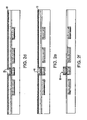
- FIGS. 1 a - 1 f are schematic diagrams of a cross-section of a first embodiment of the invention illustrating the process steps detailing the formation of a raised noble contact fabricated by blanket noble deposition and chemical mechanical planarization.
- FIGS. 2 a - 2 f are schematic diagrams of a cross-section of a second embodiment of the invention illustrating the process steps detailing the formation of a raised electrode fabricated by selective electroplating of the noble contact.
- FIGS. 3 a - 3 e are schematic diagrams of a cross-section of the MEMs switch illustrating a third embodiment of the invention for filling the electrodes of the first metal level with a noble metal using Damascene process.
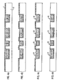
- FIGS. 4 a - 4 d are schematic diagrams of a cross-section of the MEMs switch illustrating the process steps for filling the first metal level electrodes with electroplated blanket copper metal and planarization stopping at the TaN/Ta barrier film.
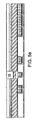
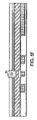
- FIGS. 5 a - 5 f are schematic diagrams of a cross-section of the MEMs showing the formation of the upper contact of the switch.
- FIGS. 6 a - 6 d are schematic diagrams showing a cross-section of the MEMs representing the process sequence for creating the upper switch contact using electroplating through a photoresist mask.
- FIGS. 7 a - 7 f are schematic diagrams showing cross-sections of the MEMs representing the process sequence to complete the device after the upper switch contact has been formed.
- a raised noble contact is formed by a blanket noble metal deposition and chemical mechanical planarization.
- a copper Damascene level is first embedded in silicon dioxide.
- the copper electrodes ( 11 , 12 , 13 , and 14 ) are capped by a silicon nitride layer ( 10 ), typically, 500-1000 ⁇ thick.
- Silicon oxide layer ( 20 ) having, preferably, a thickness of 1000-2000 ⁇ is deposited thereon, is shown in FIG. 1 a .
- Etching preferably by way of photolithography and RIE (reactive ion etching) forms a contact pattern ( 15 ) into the oxide ( 20 ) and nitride layers ( 10 ) exposing copper ( 12 ), as shown in FIG. 1 b.
- a thin barrier layer is deposited by PVD, (physical vapor deposition) or CVD (chemical vapor deposition) such as Ta, TaN, W or dual layers, such as Ta/TaN, typically 50-700 ⁇ thick (30, FIG. 1 c ).
- a blanket noble metal is deposited by PVD, CVD, or electroplating ( 40 , FIG. 1 c ).
- the noble metal is shaped by a chemical-mechanical planarization process (CMP) stopping at the barrier metal Ta, TaN, W (30, FIG. 1 d ).
- CMP chemical-mechanical planarization process
- the polish process can be stopped on the dielectric layer 20 which is not integral to the completed device.
- Noble metals that can be shaped by chemical-mechanical planarization (CMP) include Ru, Rh, Ir, Pt, and Re.
- the barrier metal ( 30 ) is removed in the field area by CMP stopping on silicon dioxide as shown in FIG. 1 e. Silicon oxide ( 20 ) is removed by reactive ion etching stopping on silicon nitride ( 10 ) to yield a raised noble metal lower electrode ( 50 , FIG. 1 f ).
- the raised electrode is formed by selective electroplating the noble contact.
- Selective electrolytic plating in the presence of a barrier layer has been discussed in U.S. Pat. No. 6,368, 484 to Volant et al. and, more specifically, the selective electro-deposition of copper in Damascene features.
- the inventive method differs in that it forms a raised noble metal contact by selective electrodeposition through a mask.
- FIG. 2 a shows that the process is initiated by way of a Damascene level that includes lower actuation electrodes ( 11 , 13 ) and lower radio frequency (RF) signal electrode ( 12 ) shown in the middle of the structure, on top of which the raised noble contact is formed. All lower electrodes are capped by silicon nitride ( 10 ) and silicon dioxide ( 20 ). Referring now to FIG. 2 b , the silicon dioxide ( 20 ) is patterned and etched by RIE leaving the copper of the middle electrode ( 12 ) exposed. A set of refractory metal barriers such as Ta, TaN, W ( 30 ) and a seed layer are then deposited by PVD or CVD methods.
- RF radio frequency
- the thin seed layer ( 35 ) is then removed in the field area by CMP or ion milling, as shown in FIG. 2 d .
- CMP CMP or ion milling
- a subsequent short chemical etch step is needed to ensure that very thin layers of metal and/or metal islands are not present on top of TaN/Ta ( 30 ) in the field area.
- the barrier film with Ta/TaN is used to pass an electric current and is followed by a selective electrodeposition in the recess containing the seed layer ( 35 ) of noble metal such as Au, AuNi, AuCo, Pd, PdNi, PdCo, Ru, Rh, Os, Pt, PtTi, Ir ( 45 ).
- the selective electrodeposition does not nucleate on the refractory Ta or TaN ( 30 ) but will only nucleate on the noble seed layer ( 35 ), as shown in FIG. 2 e .
- the Ta/TaN ( 30 ) barrier is removed by CMP in the presence of the noble contact.
- the raised contact ( 50 ) is formed by etching (RIE) the silicon oxide layer ( 20 ) down to the silicon nitride ( FIG. 2 f ).
- FIG. 3 shows the process sequence starting with a Si wafer ( 1 ), adding a silicon oxide layer ( 2 ), patterning the silicon oxide layer ( 2 ) to form the lower actuation electrodes ( 3 , 5 ) and the signal electrode ( 4 ), depositing a barrier layer by CVD or PVD methods such as TaN/Ta ( 6 ), depositing a noble metal seed layer by CVD or PVD ( 7 ) and finally blanket depositing by PVD, CVD or electroplating the noble metal ( 8 ) to fill the Damascene structures ( 3 , 4 , 5 ), planarizing the noble metal ( 8 ) by CMP to expose the barrier film ( 7 ) and finally removing the barrier film ( 7 ) from the field area by CMP resulting in lower switch electrodes ( 11 , 12 , 13 , 14 ) filled by noble
- the first metal level electrodes ( 11 , 12 , 13 , and 14 ) are filled with electroplated blanket copper metal and planarized, stopping at the barrier film TaN/Ta ( 7 ).
- the copper is recessed by chemical etching in the presence of the barrier layer TaN/Ta ( 7 ). This layer is then used to selectively electrodeposit a noble metal contact ( 21 , 22 , 23 , 24 ) on top of the recessed copper electrodes ( 11 , 12 , 13 , 14 ).
- this noble metal contact fabrication scheme there are several requirements for this noble metal contact fabrication scheme to work.
- the noble metal on top of copper needs to be not only a diffusion barrier for copper but most importantly an oxygen barrier for copper because subsequent processing steps during the MEMS switch fabrication utilize oxygen plasma to remove the sacrificial material.
- Platinum for instance, is not likely to be an oxygen barrier for copper, as described by D.E. Kotecki, et al., entitled “(Ba, Sr)TiO 3 dielectrics for future stacked-capacitor DRAM” published in IBM J Res. Dev., 43, No. 3, May 1999, pp. 367-380. Therefore, it cannot be used alone as a contact material on top of copper.
- FIG. 5 describes the formation of the upper contact.
- an organic blanket layer of sacrificial material is deposited.
- Organic material ( 60 ) such as SiLK or diamond-like-carbon (DLC)
- DLC diamond-like-carbon
- a thin refractory metal ( 90 ) is used to improve adhesion of noble metals for subsequent processing and to act as an additional hardmask for reactive ion etching.
- Metal hardmasks are deposited by PVD, CVD or IMP (ionized metal physical vapor deposition).
- FIG. 5 b shows the formation of a flat recess ( 100 ) by lithography, and the refractory metal (i.e., hardmask) ( 90 ) patterned and etched by wet etching or RIE.
- Recess ( 100 ) is formed in the sacrificial organic layer ( 60 ) by a plasma process.
- the recess process can be tailored so that the upper contact is shaped in such a way so that it results in optimum contact between the upper and the lower contact.
- the organic layer is recessed by first etching the metal hardmask layer 90 , and dielectric layers 80 and 70 with at least one RIE step. During RIE microtrenching often occurs and results in uneven etching local to the feature edge. The formation of microtrenching is used, in this application, to provide fangs at the feature edges which protrude into the organic layer. Creating small area points of contact is preferable to generate increased contact pressure for the same applied force.
- the feature is filled with a blanket noble metal layer ( 110 ) using a non-selective deposition technique, such as PVD, CVD or electroplating and CMP as shown in FIG. 5 e .
- the metal of choice for the upper contact is not necessarily the same as the noble metal of the lower contact but it is selected from the same material set, e.g., Au, AuNi, AuCo, Pd, PdNi, PdCo, Ru, Rh, Re, Os, Pt, PtTi, Ir and their alloys.
- the blanket noble metal layer is typically formed by chemical-mechanical planarization to yield the upper contact ( 110 ) but may be selectively electroplated to minimize effects of metal overburden during noble metal CMP.
- the selective electroplating process requires that there be a thin seed layer ( 101 ) deposited within the recess and in the field area on top of the hardmask ( 80 ).
- the seed layer ( 101 ) having a thickness ranging from 100 to 1000 ⁇ is then removed from the hardmask area by CMP or ion milling.
- Ruthenium, rhodium and iridium are preferred to form the seed layers for through-mask selective electroplating because there are exists CMP processes that have been developed for these three noble metals.
- Selective electroplating of the noble metal or alloy occurs only within the recess ( 100 ) and on top of the seed layer ( 101 ).
- the upper contact ( 110 ) after selective electroplating is shown in FIG. 5 f.
- a final embodiment for creating the upper switch contact is to use electroplating through a photoresist mask.
- the process sequence is described in FIG. 6 a through 6 e . Similar to the process described in FIG. 5 , after formation of the lower switch contact, an organic blanket layer of sacrificial material is deposited. The organic material ( 60 ) such as SiLK or diamond-like-carbon (DLC) is deposited. Subsequently, a thin silicon nitride layer ( 70 ) is deposited. The nitride layer ( 70 ) is patterned and etched creating a recess ( 100 ) in the organic sacrificial layer ( 60 ).
- a blanket noble metal thin seed layer ( 71 ) is deposited on top of the silicon nitride layer ( 70 ) to be used to pass electric current during noble metal electrodeposition.
- a photoresist mask ( 72 ) is applied on top of the noble seed layer ( 71 ), as shown in FIG. 6 a .
- the upper contact ( 110 ) is then formed by selectively electroplating where the photoresist mask has exposed the thin noble metal seed layer, as shown in FIG. 6 c .
- the photoresist mask ( 72 ) is then stripped off ( FIG. 6 c ) and the remaining noble metal seed layer ( 71 ) is removed by ion milling or chemical etching ( FIG. 6 d ).
- the organic layer ( 60 ) and dielectric layers ( 70 , 80 ) are then patterned and backfilled with additional dielectric ( 200 ) and planarized with CMP as shown in FIG. 7 a.
- a Dual Damascene copper level is formed in dielectric layers ( 220 , 240 and 200 ) and capped with silicon nitride ( 260 ) as shown in FIG. 7 b.
- the planar structure is then patterned and RIE'ed to open the dielectric stack layers ( 70 , 80 , 220 , 240 and 260 ) to expose the organic layer ( 60 ).
- Additional organic material 300 is then deposited capped with silicon nitride ( 320 ) and patterned by RIE to produce the cross section shown in FIG. 7C .
- a backfill dielectric ( 400 ) is then deposited and planarized and additional dielectric ( 420 ) is deposited on the planar surface as shown in FIG. 7 d.
- Access vias are now formed in the dielectric layer ( 420 ) exposing the organic layer ( 300 ) to facilitate device release.
- the sample is then exposed to an oxygen ash which removes organic layers ( 300 , 60 ).
- the device is then sealed by depositing a pinch-off layer ( 500 ) and a final series of lithography and RIE are used to form contact ( 600 ) for wire bonding or solder ball chip formation.
- it is preferred that the switch is fully encapsulated in an inert environment with He, N 2 , Kr, Ne, or Ar gas.
Landscapes
- Chemical & Material Sciences (AREA)
- Engineering & Computer Science (AREA)
- Composite Materials (AREA)
- Materials Engineering (AREA)
- Micromachines (AREA)
- Internal Circuitry In Semiconductor Integrated Circuit Devices (AREA)
- Manufacture Of Switches (AREA)
Abstract
Description
-
- 1) different metallurgy on each side of the contact
- lattice mismatch reduces adhesion, and
- 2) optimized hardness of the metals in contact
- harder metal is expected to give lower adhesion.
- 1) different metallurgy on each side of the contact
Claims (7)
Priority Applications (1)
| Application Number | Priority Date | Filing Date | Title |
|---|---|---|---|
| US11/358,823 US7581314B2 (en) | 2003-07-08 | 2006-02-21 | Method of forming noble metal contacts |
Applications Claiming Priority (2)
| Application Number | Priority Date | Filing Date | Title |
|---|---|---|---|
| US10/604,278 US7202764B2 (en) | 2003-07-08 | 2003-07-08 | Noble metal contacts for micro-electromechanical switches |
| US11/358,823 US7581314B2 (en) | 2003-07-08 | 2006-02-21 | Method of forming noble metal contacts |
Related Parent Applications (1)
| Application Number | Title | Priority Date | Filing Date |
|---|---|---|---|
| US10/604,278 Division US7202764B2 (en) | 2003-07-08 | 2003-07-08 | Noble metal contacts for micro-electromechanical switches |
Publications (2)
| Publication Number | Publication Date |
|---|---|
| US20060164194A1 US20060164194A1 (en) | 2006-07-27 |
| US7581314B2 true US7581314B2 (en) | 2009-09-01 |
Family
ID=33564148
Family Applications (2)
| Application Number | Title | Priority Date | Filing Date |
|---|---|---|---|
| US10/604,278 Expired - Lifetime US7202764B2 (en) | 2003-07-08 | 2003-07-08 | Noble metal contacts for micro-electromechanical switches |
| US11/358,823 Expired - Fee Related US7581314B2 (en) | 2003-07-08 | 2006-02-21 | Method of forming noble metal contacts |
Family Applications Before (1)
| Application Number | Title | Priority Date | Filing Date |
|---|---|---|---|
| US10/604,278 Expired - Lifetime US7202764B2 (en) | 2003-07-08 | 2003-07-08 | Noble metal contacts for micro-electromechanical switches |
Country Status (8)
| Country | Link |
|---|---|
| US (2) | US7202764B2 (en) |
| EP (1) | EP1642312B1 (en) |
| JP (1) | JP4516960B2 (en) |
| KR (1) | KR100861680B1 (en) |
| CN (1) | CN100424804C (en) |
| IL (1) | IL173017A0 (en) |
| TW (1) | TWI312527B (en) |
| WO (1) | WO2005006372A1 (en) |
Cited By (3)
| Publication number | Priority date | Publication date | Assignee | Title |
|---|---|---|---|---|
| US8493081B2 (en) | 2009-12-08 | 2013-07-23 | Magna Closures Inc. | Wide activation angle pinch sensor section and sensor hook-on attachment principle |
| US9000556B2 (en) | 2011-10-07 | 2015-04-07 | International Business Machines Corporation | Lateral etch stop for NEMS release etch for high density NEMS/CMOS monolithic integration |
| US9234979B2 (en) | 2009-12-08 | 2016-01-12 | Magna Closures Inc. | Wide activation angle pinch sensor section |
Families Citing this family (36)
| Publication number | Priority date | Publication date | Assignee | Title |
|---|---|---|---|---|
| US7132306B1 (en) * | 2003-12-08 | 2006-11-07 | Advanced Micro Devices, Inc. | Method of forming an interlevel dielectric layer employing dielectric etch-back process without extra mask set |
| DE102004005022B4 (en) * | 2004-01-30 | 2006-02-16 | Infineon Technologies Ag | Process for the production of metal interconnects on electronic components |
| US7688095B2 (en) * | 2004-07-30 | 2010-03-30 | International Business Machines Corporation | Interposer structures and methods of manufacturing the same |
| US8193606B2 (en) * | 2005-02-28 | 2012-06-05 | Semiconductor Energy Laboratory Co., Ltd. | Semiconductor device including a memory element |
| US7288464B2 (en) * | 2005-04-11 | 2007-10-30 | Hewlett-Packard Development Company, L.P. | MEMS packaging structure and methods |
| US20060234412A1 (en) * | 2005-04-19 | 2006-10-19 | Hewlett-Packard Development Company, L.P. Intellectual Property Administration | MEMS release methods |
| JP2009510707A (en) * | 2005-10-03 | 2009-03-12 | アナログ デバイシス, インコーポレイテッド | MEMS switch contact system |
| US7968364B2 (en) * | 2005-10-03 | 2011-06-28 | Analog Devices, Inc. | MEMS switch capping and passivation method |
| US7666698B2 (en) * | 2006-03-21 | 2010-02-23 | Freescale Semiconductor, Inc. | Method for forming and sealing a cavity for an integrated MEMS device |
| EP2122648B1 (en) * | 2006-12-22 | 2012-06-27 | Analog Devices, Inc. | Method and apparatus for driving a switch |
| US20100018843A1 (en) * | 2008-07-24 | 2010-01-28 | General Electric Company | Low work function electrical component |
| US7943410B2 (en) * | 2008-12-10 | 2011-05-17 | Stmicroelectronics, Inc. | Embedded microelectromechanical systems (MEMS) semiconductor substrate and related method of forming |
| US8189292B2 (en) * | 2008-12-24 | 2012-05-29 | Hitachi Global Storage Technologies Netherlands B.V. | Method for manufacturing a magnetic write head having a write pole with a trailing edge taper using a Rieable hard mask |
| US8445306B2 (en) * | 2008-12-24 | 2013-05-21 | International Business Machines Corporation | Hybrid MEMS RF switch and method of fabricating same |
| WO2011053346A1 (en) | 2009-10-26 | 2011-05-05 | Northwestern University | Microelectromechanical device and system |
| JP2011259371A (en) * | 2010-06-11 | 2011-12-22 | Canon Inc | Manufacturing method of capacitive electromechanical transducer |
| US8535966B2 (en) | 2010-07-27 | 2013-09-17 | International Business Machines Corporation | Horizontal coplanar switches and methods of manufacture |
| US20120194306A1 (en) * | 2011-02-01 | 2012-08-02 | Maxim Integrated Products, Inc. | Preventing contact stiction in micro relays |
| US9708177B2 (en) * | 2011-09-02 | 2017-07-18 | Cavendish Kinetics, Inc. | MEMS device anchoring |
| US9740343B2 (en) | 2012-04-13 | 2017-08-22 | Apple Inc. | Capacitive sensing array modulation |
| US9030440B2 (en) | 2012-05-18 | 2015-05-12 | Apple Inc. | Capacitive sensor packaging |
| CN103723674B (en) * | 2012-10-16 | 2016-02-17 | 国际商业机器公司 | MEMS transistor and manufacture method thereof |
| US8927312B2 (en) | 2012-10-16 | 2015-01-06 | International Business Machines Corporation | Method of fabricating MEMS transistors on far back end of line |
| US9883822B2 (en) | 2013-06-05 | 2018-02-06 | Apple Inc. | Biometric sensor chip having distributed sensor and control circuitry |
| NL2012891B1 (en) | 2013-06-05 | 2016-06-21 | Apple Inc | Biometric sensor chip having distributed sensor and control circuitry. |
| US9984270B2 (en) | 2013-08-05 | 2018-05-29 | Apple Inc. | Fingerprint sensor in an electronic device |
| US9460332B1 (en) | 2013-09-09 | 2016-10-04 | Apple Inc. | Capacitive fingerprint sensor including an electrostatic lens |
| US10296773B2 (en) | 2013-09-09 | 2019-05-21 | Apple Inc. | Capacitive sensing array having electrical isolation |
| US9697409B2 (en) | 2013-09-10 | 2017-07-04 | Apple Inc. | Biometric sensor stack structure |
| US9563233B2 (en) * | 2014-08-14 | 2017-02-07 | Microsoft Technology Licensing, Llc | Electronic device with plated electrical contact |
| CN104567994B (en) * | 2014-12-18 | 2017-03-08 | 河海大学 | The contact resistance of MEMS material and contact force synchro measure structure and method |
| US20160222833A1 (en) * | 2015-02-03 | 2016-08-04 | Borgwarner Inc. | Waste heat recovery system layout and packaging strategy |
| US9466452B1 (en) * | 2015-03-31 | 2016-10-11 | Stmicroelectronics, Inc. | Integrated cantilever switch |
| US9845235B2 (en) | 2015-09-03 | 2017-12-19 | General Electric Company | Refractory seed metal for electroplated MEMS structures |
| RU2666180C2 (en) * | 2016-01-26 | 2018-09-06 | Акционерное общество "Научно-исследовательский институт полупроводниковых приборов" (АО "НИИПП") | Method of manufacturing rectifying contacts to gallium arsenide by electrochemical deposition of ruthenium |
| US10950444B2 (en) * | 2018-01-30 | 2021-03-16 | Tokyo Electron Limited | Metal hard mask layers for processing of microelectronic workpieces |
Citations (3)
| Publication number | Priority date | Publication date | Assignee | Title |
|---|---|---|---|---|
| US5662788A (en) * | 1996-06-03 | 1997-09-02 | Micron Technology, Inc. | Method for forming a metallization layer |
| US6383920B1 (en) * | 2001-01-10 | 2002-05-07 | International Business Machines Corporation | Process of enclosing via for improved reliability in dual damascene interconnects |
| US6610596B1 (en) * | 1999-09-15 | 2003-08-26 | Samsung Electronics Co., Ltd. | Method of forming metal interconnection using plating and semiconductor device manufactured by the method |
Family Cites Families (20)
| Publication number | Priority date | Publication date | Assignee | Title |
|---|---|---|---|---|
| GB2095911B (en) * | 1981-03-17 | 1985-02-13 | Standard Telephones Cables Ltd | Electrical switch device |
| US5258591A (en) * | 1991-10-18 | 1993-11-02 | Westinghouse Electric Corp. | Low inductance cantilever switch |
| JPH06131938A (en) * | 1992-10-16 | 1994-05-13 | Omron Corp | Electric switchgear |
| US5479042A (en) * | 1993-02-01 | 1995-12-26 | Brooktree Corporation | Micromachined relay and method of forming the relay |
| JP3246841B2 (en) * | 1994-03-31 | 2002-01-15 | 日東電工株式会社 | Probe structure |
| CA2211830C (en) * | 1997-08-22 | 2002-08-13 | Cindy Xing Qiu | Miniature electromagnetic microwave switches and switch arrays |
| US5959338A (en) | 1997-12-29 | 1999-09-28 | Honeywell Inc. | Micro electro-mechanical systems relay |
| JPH11250792A (en) * | 1998-03-03 | 1999-09-17 | Nippon Telegr & Teleph Corp <Ntt> | Electrostatic switch element |
| US6054659A (en) * | 1998-03-09 | 2000-04-25 | General Motors Corporation | Integrated electrostatically-actuated micromachined all-metal micro-relays |
| JP2000311572A (en) * | 1999-04-27 | 2000-11-07 | Omron Corp | Electrostatic relay |
| US6057520A (en) * | 1999-06-30 | 2000-05-02 | Mcnc | Arc resistant high voltage micromachined electrostatic switch |
| JP2001043762A (en) * | 1999-07-29 | 2001-02-16 | Fujitsu Takamisawa Component Ltd | Electrical contact, manufacture thereof, and reed switch |
| US6307452B1 (en) * | 1999-09-16 | 2001-10-23 | Motorola, Inc. | Folded spring based micro electromechanical (MEM) RF switch |
| US6124650A (en) * | 1999-10-15 | 2000-09-26 | Lucent Technologies Inc. | Non-volatile MEMS micro-relays using magnetic actuators |
| US6310339B1 (en) * | 1999-10-28 | 2001-10-30 | Hrl Laboratories, Llc | Optically controlled MEM switches |
| US6396368B1 (en) * | 1999-11-10 | 2002-05-28 | Hrl Laboratories, Llc | CMOS-compatible MEM switches and method of making |
| AU2001249055A1 (en) * | 2000-02-02 | 2001-08-14 | Raytheon Company | Microelectromechanical micro-relay with liquid metal contacts |
| US6489857B2 (en) * | 2000-11-30 | 2002-12-03 | International Business Machines Corporation | Multiposition micro electromechanical switch |
| CN1127106C (en) * | 2001-01-21 | 2003-11-05 | 北京大学 | Radio frequency micro electromechanical system switch of silicon, metal and medium film bridge |
| US6635506B2 (en) * | 2001-11-07 | 2003-10-21 | International Business Machines Corporation | Method of fabricating micro-electromechanical switches on CMOS compatible substrates |
-
2003
- 2003-07-08 US US10/604,278 patent/US7202764B2/en not_active Expired - Lifetime
-
2004
- 2004-06-02 KR KR1020067000001A patent/KR100861680B1/en not_active Expired - Fee Related
- 2004-06-02 CN CNB2004800192330A patent/CN100424804C/en not_active Expired - Fee Related
- 2004-06-02 JP JP2006518191A patent/JP4516960B2/en not_active Expired - Fee Related
- 2004-06-02 WO PCT/EP2004/050940 patent/WO2005006372A1/en not_active Ceased
- 2004-06-02 EP EP04741661A patent/EP1642312B1/en not_active Expired - Lifetime
- 2004-07-01 TW TW093119921A patent/TWI312527B/en not_active IP Right Cessation
-
2006
- 2006-01-08 IL IL173017A patent/IL173017A0/en unknown
- 2006-02-21 US US11/358,823 patent/US7581314B2/en not_active Expired - Fee Related
Patent Citations (3)
| Publication number | Priority date | Publication date | Assignee | Title |
|---|---|---|---|---|
| US5662788A (en) * | 1996-06-03 | 1997-09-02 | Micron Technology, Inc. | Method for forming a metallization layer |
| US6610596B1 (en) * | 1999-09-15 | 2003-08-26 | Samsung Electronics Co., Ltd. | Method of forming metal interconnection using plating and semiconductor device manufactured by the method |
| US6383920B1 (en) * | 2001-01-10 | 2002-05-07 | International Business Machines Corporation | Process of enclosing via for improved reliability in dual damascene interconnects |
Non-Patent Citations (5)
| Title |
|---|
| "(Ba,Sr) TiO3 dielectrics for future stacked-capacitor DRAM" by D.E. Kotecki, J.D. Baniecki, H. Shen, R.B. Laibowitz, K.L. Saenger, J.J. Lian, T.M. Shaw, S.D. Athavale, C. Cabral, Jr., P.R. Duncombe, M. Gutsche, G. Kunkel, Y.-J. Park, Y.-Y. Wang, R. Wise, IBM J. Res, Develop. VO1 43 No. 3 May 1999. |
| "Micromechanical Switches Fabricated Using Nickel Surface Micromachining" Paul M. Zavracky, Sumit Majumder, and Nicol E. McGruer, Journal of Microelectromechanical Systems, vol. 6, No. 1, Mar. 1997. |
| "Microswitches and Microrelays with a View Toward Microwave Applications" Paul M. Zavracky, Nicol E. McGruer, Richard H. Morrison, David Potter, Northeastern University, Boston, Massachusetts 02115, Analog Devices Wilmington, Massachusetts 01887, Date: 1999. |
| "RF Mems Switches adn Switch Circuits" Gabriel M. Rebeiz, Jeremy B. Muldavin, IEEE Microwave Magazine, Dec. 2001 pp. 59-71. |
| IBM U.S. Appl. No. 60/339,089, filed Dec. 10, 2001, Christopher Jahnes, et al. |
Cited By (5)
| Publication number | Priority date | Publication date | Assignee | Title |
|---|---|---|---|---|
| US8493081B2 (en) | 2009-12-08 | 2013-07-23 | Magna Closures Inc. | Wide activation angle pinch sensor section and sensor hook-on attachment principle |
| US9234979B2 (en) | 2009-12-08 | 2016-01-12 | Magna Closures Inc. | Wide activation angle pinch sensor section |
| US9417099B2 (en) | 2009-12-08 | 2016-08-16 | Magna Closures Inc. | Wide activation angle pinch sensor section |
| US9000556B2 (en) | 2011-10-07 | 2015-04-07 | International Business Machines Corporation | Lateral etch stop for NEMS release etch for high density NEMS/CMOS monolithic integration |
| US9162877B2 (en) | 2011-10-07 | 2015-10-20 | Globalfoundries U.S. 2 Llc | Lateral etch stop for NEMS release etch for high density NEMS/CMOS monolithic integration |
Also Published As
| Publication number | Publication date |
|---|---|
| TW200514112A (en) | 2005-04-16 |
| KR20060036438A (en) | 2006-04-28 |
| KR100861680B1 (en) | 2008-10-07 |
| TWI312527B (en) | 2009-07-21 |
| CN1816890A (en) | 2006-08-09 |
| US20050007217A1 (en) | 2005-01-13 |
| US20060164194A1 (en) | 2006-07-27 |
| EP1642312B1 (en) | 2012-11-28 |
| EP1642312A1 (en) | 2006-04-05 |
| US7202764B2 (en) | 2007-04-10 |
| JP2009514142A (en) | 2009-04-02 |
| IL173017A0 (en) | 2006-06-11 |
| WO2005006372A1 (en) | 2005-01-20 |
| CN100424804C (en) | 2008-10-08 |
| JP4516960B2 (en) | 2010-08-04 |
Similar Documents
| Publication | Publication Date | Title |
|---|---|---|
| US7581314B2 (en) | Method of forming noble metal contacts | |
| US6701779B2 (en) | Perpendicular torsion micro-electromechanical switch | |
| EP1461828B1 (en) | Method of fabricating micro-electromechanical switches on cmos compatible substrates | |
| US6621392B1 (en) | Micro electromechanical switch having self-aligned spacers | |
| US7256670B2 (en) | Diaphragm activated micro-electromechanical switch | |
| US7348870B2 (en) | Structure and method of fabricating a hinge type MEMS switch | |
| US9000562B2 (en) | Flexible processing method for metal-insulator-metal capacitor formation | |
| CN101213631B (en) | Capacitive rf-mems device and its manufacture method | |
| JP2004167671A (en) | Encapsulated mems structure and method of manufacturing the same | |
| US8054148B2 (en) | Contact material, device including contact material, and method of making | |
| JP4317015B2 (en) | Metal-to-metal antifuses using carbon-containing antifuse materials | |
| JP4772302B2 (en) | Micro-electromechanical system and manufacturing method thereof | |
| US20060274470A1 (en) | Contact material, device including contact material, and method of making | |
| WO2003107372A1 (en) | Micro-electromechanical switch having a deformable elastomeric conductive element | |
| EP1920493B1 (en) | Micro-cavity mems device and method of fabricating same | |
| JPH09162187A (en) | Semiconductor device and manufacturing method thereof | |
| KR20030001646A (en) | Method for manufacturing capacitor of semiconductor device |
Legal Events
| Date | Code | Title | Description |
|---|---|---|---|
| FEPP | Fee payment procedure |
Free format text: PAYOR NUMBER ASSIGNED (ORIGINAL EVENT CODE: ASPN); ENTITY STATUS OF PATENT OWNER: LARGE ENTITY |
|
| STCF | Information on status: patent grant |
Free format text: PATENTED CASE |
|
| CC | Certificate of correction | ||
| REMI | Maintenance fee reminder mailed | ||
| FPAY | Fee payment |
Year of fee payment: 4 |
|
| SULP | Surcharge for late payment | ||
| AS | Assignment |
Owner name: GLOBALFOUNDRIES U.S. 2 LLC, NEW YORK Free format text: ASSIGNMENT OF ASSIGNORS INTEREST;ASSIGNOR:INTERNATIONAL BUSINESS MACHINES CORPORATION;REEL/FRAME:036550/0001 Effective date: 20150629 |
|
| AS | Assignment |
Owner name: GLOBALFOUNDRIES INC., CAYMAN ISLANDS Free format text: ASSIGNMENT OF ASSIGNORS INTEREST;ASSIGNORS:GLOBALFOUNDRIES U.S. 2 LLC;GLOBALFOUNDRIES U.S. INC.;REEL/FRAME:036779/0001 Effective date: 20150910 |
|
| FPAY | Fee payment |
Year of fee payment: 8 |
|
| AS | Assignment |
Owner name: WILMINGTON TRUST, NATIONAL ASSOCIATION, DELAWARE Free format text: SECURITY AGREEMENT;ASSIGNOR:GLOBALFOUNDRIES INC.;REEL/FRAME:049490/0001 Effective date: 20181127 |
|
| AS | Assignment |
Owner name: GLOBALFOUNDRIES U.S. INC., CALIFORNIA Free format text: ASSIGNMENT OF ASSIGNORS INTEREST;ASSIGNOR:GLOBALFOUNDRIES INC.;REEL/FRAME:054633/0001 Effective date: 20201022 |
|
| AS | Assignment |
Owner name: GLOBALFOUNDRIES INC., CAYMAN ISLANDS Free format text: RELEASE BY SECURED PARTY;ASSIGNOR:WILMINGTON TRUST, NATIONAL ASSOCIATION;REEL/FRAME:054636/0001 Effective date: 20201117 |
|
| FEPP | Fee payment procedure |
Free format text: MAINTENANCE FEE REMINDER MAILED (ORIGINAL EVENT CODE: REM.); ENTITY STATUS OF PATENT OWNER: LARGE ENTITY |
|
| AS | Assignment |
Owner name: GLOBALFOUNDRIES U.S. INC., NEW YORK Free format text: RELEASE BY SECURED PARTY;ASSIGNOR:WILMINGTON TRUST, NATIONAL ASSOCIATION;REEL/FRAME:056987/0001 Effective date: 20201117 Owner name: GLOBALFOUNDRIES U.S. INC., NEW YORK Free format text: RELEASE OF SECURITY INTEREST;ASSIGNOR:WILMINGTON TRUST, NATIONAL ASSOCIATION;REEL/FRAME:056987/0001 Effective date: 20201117 |
|
| LAPS | Lapse for failure to pay maintenance fees |
Free format text: PATENT EXPIRED FOR FAILURE TO PAY MAINTENANCE FEES (ORIGINAL EVENT CODE: EXP.); ENTITY STATUS OF PATENT OWNER: LARGE ENTITY |
|
| STCH | Information on status: patent discontinuation |
Free format text: PATENT EXPIRED DUE TO NONPAYMENT OF MAINTENANCE FEES UNDER 37 CFR 1.362 |
|
| FP | Lapsed due to failure to pay maintenance fee |
Effective date: 20210901 |