US7554255B2 - Electric field emission device having a triode structure fabricated by using an anodic oxidation process and method for fabricating same - Google Patents
Electric field emission device having a triode structure fabricated by using an anodic oxidation process and method for fabricating same Download PDFInfo
- Publication number
- US7554255B2 US7554255B2 US10/522,572 US52257205A US7554255B2 US 7554255 B2 US7554255 B2 US 7554255B2 US 52257205 A US52257205 A US 52257205A US 7554255 B2 US7554255 B2 US 7554255B2
- Authority
- US
- United States
- Prior art keywords
- sub
- layer
- micro holes
- electrode layer
- carbon nano
- Prior art date
- Legal status (The legal status is an assumption and is not a legal conclusion. Google has not performed a legal analysis and makes no representation as to the accuracy of the status listed.)
- Expired - Fee Related, expires
Links
- 238000000034 method Methods 0.000 title claims abstract description 93
- 230000008569 process Effects 0.000 title claims abstract description 43
- 230000005684 electric field Effects 0.000 title claims abstract description 39
- 230000003647 oxidation Effects 0.000 title claims abstract description 29
- 238000007254 oxidation reaction Methods 0.000 title claims abstract description 29
- 239000000758 substrate Substances 0.000 claims abstract description 16
- 238000007789 sealing Methods 0.000 claims abstract description 9
- PNEYBMLMFCGWSK-UHFFFAOYSA-N aluminium oxide Inorganic materials [O-2].[O-2].[O-2].[Al+3].[Al+3] PNEYBMLMFCGWSK-UHFFFAOYSA-N 0.000 claims description 37
- 229910052751 metal Inorganic materials 0.000 claims description 32
- 239000002184 metal Substances 0.000 claims description 32
- 229910052782 aluminium Inorganic materials 0.000 claims description 23
- XAGFODPZIPBFFR-UHFFFAOYSA-N aluminium Chemical compound [Al] XAGFODPZIPBFFR-UHFFFAOYSA-N 0.000 claims description 20
- OKTJSMMVPCPJKN-UHFFFAOYSA-N Carbon Chemical compound [C] OKTJSMMVPCPJKN-UHFFFAOYSA-N 0.000 claims description 16
- 239000002041 carbon nanotube Substances 0.000 claims description 16
- 229910021393 carbon nanotube Inorganic materials 0.000 claims description 16
- NBIIXXVUZAFLBC-UHFFFAOYSA-N Phosphoric acid Chemical compound OP(O)(O)=O NBIIXXVUZAFLBC-UHFFFAOYSA-N 0.000 claims description 14
- 239000000203 mixture Substances 0.000 claims description 12
- 239000002717 carbon nanostructure Substances 0.000 claims description 10
- 239000000243 solution Substances 0.000 claims description 10
- MUBZPKHOEPUJKR-UHFFFAOYSA-N Oxalic acid Chemical compound OC(=O)C(O)=O MUBZPKHOEPUJKR-UHFFFAOYSA-N 0.000 claims description 9
- VYPSYNLAJGMNEJ-UHFFFAOYSA-N Silicium dioxide Chemical compound O=[Si]=O VYPSYNLAJGMNEJ-UHFFFAOYSA-N 0.000 claims description 8
- 230000004888 barrier function Effects 0.000 claims description 8
- 238000004518 low pressure chemical vapour deposition Methods 0.000 claims description 8
- 229910000147 aluminium phosphate Inorganic materials 0.000 claims description 7
- 239000002134 carbon nanofiber Substances 0.000 claims description 7
- 239000011852 carbon nanoparticle Substances 0.000 claims description 7
- 229910044991 metal oxide Inorganic materials 0.000 claims description 7
- VNWKTOKETHGBQD-UHFFFAOYSA-N methane Chemical compound C VNWKTOKETHGBQD-UHFFFAOYSA-N 0.000 claims description 7
- 238000004544 sputter deposition Methods 0.000 claims description 7
- QAOWNCQODCNURD-UHFFFAOYSA-N Sulfuric acid Chemical compound OS(O)(=O)=O QAOWNCQODCNURD-UHFFFAOYSA-N 0.000 claims description 6
- 238000000313 electron-beam-induced deposition Methods 0.000 claims description 6
- 238000005530 etching Methods 0.000 claims description 6
- QAOWNCQODCNURD-UHFFFAOYSA-L Sulfate Chemical compound [O-]S([O-])(=O)=O QAOWNCQODCNURD-UHFFFAOYSA-L 0.000 claims description 5
- KRVSOGSZCMJSLX-UHFFFAOYSA-L chromic acid Substances O[Cr](O)(=O)=O KRVSOGSZCMJSLX-UHFFFAOYSA-L 0.000 claims description 5
- 238000009713 electroplating Methods 0.000 claims description 5
- AWJWCTOOIBYHON-UHFFFAOYSA-N furo[3,4-b]pyrazine-5,7-dione Chemical compound C1=CN=C2C(=O)OC(=O)C2=N1 AWJWCTOOIBYHON-UHFFFAOYSA-N 0.000 claims description 5
- 239000007789 gas Substances 0.000 claims description 5
- 229910001510 metal chloride Inorganic materials 0.000 claims description 5
- 229910001960 metal nitrate Inorganic materials 0.000 claims description 5
- 238000000992 sputter etching Methods 0.000 claims description 5
- 239000000126 substance Substances 0.000 claims description 5
- 238000002207 thermal evaporation Methods 0.000 claims description 5
- 238000001039 wet etching Methods 0.000 claims description 5
- 239000004215 Carbon black (E152) Substances 0.000 claims description 4
- 229910052681 coesite Inorganic materials 0.000 claims description 4
- 229910052906 cristobalite Inorganic materials 0.000 claims description 4
- 238000001312 dry etching Methods 0.000 claims description 4
- 229930195733 hydrocarbon Natural products 0.000 claims description 4
- 150000002430 hydrocarbons Chemical class 0.000 claims description 4
- 239000004065 semiconductor Substances 0.000 claims description 4
- 239000000377 silicon dioxide Substances 0.000 claims description 4
- 229910052682 stishovite Inorganic materials 0.000 claims description 4
- 230000001131 transforming effect Effects 0.000 claims description 4
- 229910052905 tridymite Inorganic materials 0.000 claims description 4
- UGFAIRIUMAVXCW-UHFFFAOYSA-N Carbon monoxide Chemical compound [O+]#[C-] UGFAIRIUMAVXCW-UHFFFAOYSA-N 0.000 claims description 3
- UFHFLCQGNIYNRP-UHFFFAOYSA-N Hydrogen Chemical compound [H][H] UFHFLCQGNIYNRP-UHFFFAOYSA-N 0.000 claims description 3
- 230000003213 activating effect Effects 0.000 claims description 3
- 239000002194 amorphous carbon material Substances 0.000 claims description 3
- 229910002091 carbon monoxide Inorganic materials 0.000 claims description 3
- 238000000151 deposition Methods 0.000 claims description 3
- 238000007772 electroless plating Methods 0.000 claims description 3
- 229910052739 hydrogen Inorganic materials 0.000 claims description 3
- 239000001257 hydrogen Substances 0.000 claims description 3
- 235000006408 oxalic acid Nutrition 0.000 claims description 3
- 238000007598 dipping method Methods 0.000 claims description 2
- 239000011259 mixed solution Substances 0.000 claims description 2
- 229910003481 amorphous carbon Inorganic materials 0.000 claims 4
- 239000003575 carbonaceous material Substances 0.000 claims 4
- 238000005979 thermal decomposition reaction Methods 0.000 claims 4
- 238000000354 decomposition reaction Methods 0.000 claims 2
- 239000003792 electrolyte Substances 0.000 claims 2
- 238000007747 plating Methods 0.000 claims 2
- 230000003247 decreasing effect Effects 0.000 abstract description 2
- 229910052804 chromium Inorganic materials 0.000 description 5
- 239000000463 material Substances 0.000 description 4
- 229910052758 niobium Inorganic materials 0.000 description 4
- 229910052719 titanium Inorganic materials 0.000 description 4
- 229910052721 tungsten Inorganic materials 0.000 description 4
- XUIMIQQOPSSXEZ-UHFFFAOYSA-N Silicon Chemical compound [Si] XUIMIQQOPSSXEZ-UHFFFAOYSA-N 0.000 description 3
- NINIDFKCEFEMDL-UHFFFAOYSA-N Sulfur Chemical compound [S] NINIDFKCEFEMDL-UHFFFAOYSA-N 0.000 description 3
- UCKMPCXJQFINFW-UHFFFAOYSA-N Sulphide Chemical compound [S-2] UCKMPCXJQFINFW-UHFFFAOYSA-N 0.000 description 3
- 229920001940 conductive polymer Polymers 0.000 description 3
- 229910052750 molybdenum Inorganic materials 0.000 description 3
- 150000004767 nitrides Chemical class 0.000 description 3
- 229910052710 silicon Inorganic materials 0.000 description 3
- 239000010703 silicon Substances 0.000 description 3
- 229910052717 sulfur Inorganic materials 0.000 description 3
- 239000011593 sulfur Substances 0.000 description 3
- GWEVSGVZZGPLCZ-UHFFFAOYSA-N Titan oxide Chemical compound O=[Ti]=O GWEVSGVZZGPLCZ-UHFFFAOYSA-N 0.000 description 2
- 239000000956 alloy Substances 0.000 description 2
- 229910045601 alloy Inorganic materials 0.000 description 2
- 230000015572 biosynthetic process Effects 0.000 description 2
- 230000003197 catalytic effect Effects 0.000 description 2
- 238000010894 electron beam technology Methods 0.000 description 2
- 239000011521 glass Substances 0.000 description 2
- 229910052737 gold Inorganic materials 0.000 description 2
- 239000010931 gold Substances 0.000 description 2
- 238000001020 plasma etching Methods 0.000 description 2
- 239000002861 polymer material Substances 0.000 description 2
- 230000004044 response Effects 0.000 description 2
- 229910052715 tantalum Inorganic materials 0.000 description 2
- 239000002253 acid Substances 0.000 description 1
- 229910052788 barium Inorganic materials 0.000 description 1
- 229910052792 caesium Inorganic materials 0.000 description 1
- 239000004020 conductor Substances 0.000 description 1
- 230000000694 effects Effects 0.000 description 1
- 238000005566 electron beam evaporation Methods 0.000 description 1
- 125000000524 functional group Chemical group 0.000 description 1
- PCHJSUWPFVWCPO-UHFFFAOYSA-N gold Chemical compound [Au] PCHJSUWPFVWCPO-UHFFFAOYSA-N 0.000 description 1
- 230000004048 modification Effects 0.000 description 1
- 238000012986 modification Methods 0.000 description 1
- 229910052759 nickel Inorganic materials 0.000 description 1
- 229910052697 platinum Inorganic materials 0.000 description 1
- 238000005546 reactive sputtering Methods 0.000 description 1
- 230000005641 tunneling Effects 0.000 description 1
- 229910052720 vanadium Inorganic materials 0.000 description 1
- 229910052726 zirconium Inorganic materials 0.000 description 1
Images


Classifications
-
- H—ELECTRICITY
- H01—ELECTRIC ELEMENTS
- H01J—ELECTRIC DISCHARGE TUBES OR DISCHARGE LAMPS
- H01J21/00—Vacuum tubes
- H01J21/02—Tubes with a single discharge path
- H01J21/06—Tubes with a single discharge path having electrostatic control means only
- H01J21/10—Tubes with a single discharge path having electrostatic control means only with one or more immovable internal control electrodes, e.g. triode, pentode, octode
- H01J21/105—Tubes with a single discharge path having electrostatic control means only with one or more immovable internal control electrodes, e.g. triode, pentode, octode with microengineered cathode and control electrodes, e.g. Spindt-type
-
- H—ELECTRICITY
- H01—ELECTRIC ELEMENTS
- H01J—ELECTRIC DISCHARGE TUBES OR DISCHARGE LAMPS
- H01J9/00—Apparatus or processes specially adapted for the manufacture, installation, removal, maintenance of electric discharge tubes, discharge lamps, or parts thereof; Recovery of material from discharge tubes or lamps
- H01J9/02—Manufacture of electrodes or electrode systems
- H01J9/022—Manufacture of electrodes or electrode systems of cold cathodes
- H01J9/025—Manufacture of electrodes or electrode systems of cold cathodes of field emission cathodes
Definitions
- the present invention relates to an electric field emission device and a method for fabricating same; and, more particularly, to an electric field emission device having a triode structure fabricated by using an anodic oxidation process and a method for fabricating same.
- an electric field emission device means a device where electrons are emitted from a surface of metal or semiconductor in a vacuum in accordance with tunneling effect caused by applying electronic field having high intensity to the surface.
- Such an electric field emission device may be utilized as a high-speed switching device, a microwave generator, an amplifier or a display device.
- the emitted electrons can induce high power at a high frequency in a vacuum with low energy loss.
- the device has several advantages that it has a shorter response time than a conventional solid-state device and may be integrated on a single silicon chip.
- FIG. 1 illustrates a cross-sectional view of a conventional “Spindt” type electric field emission device having a triode structure fabricated by using an electron beam photolithographic process.
- the electric field emission device is fabricated as follows. That is, on a glass or a silicon substrate 100 , a cathode layer 102 , a resistive layer 104 , an insulating layer 106 and a gate electrode layer 108 are formed sequentially. And then, photosensitive film patterns, each having a diameter of micrometer, are formed on the gate electrode 108 by using a photolithographic process. Thereafter, the insulating layer 106 is etched by using a reactive ion etching technique such that a surface of the resistive layer 104 is exposed. Subsequently, a metal electric field emission tip 110 containing material such as Mo, W and Cr is vertically deposited on the resistive layer 104 to have a conical shape by using an electron beam evaporation technique.
- the Spindt type electric field emission device has advantages that it has a shorter response time than a conventional solid-state device and may be integrated on a single silicon chip.
- it is difficult to arrange a plurality of micro holes at regular intervals on the electric field emission device as shown in FIG. 1 , particularly when an area of the surface of the device is large.
- the electric field emission device as shown in FIG. 1 has a disadvantage that it requires a high driving voltage.
- there may be needed an additional process to form micro holes, each having a sub-micrometer diameter, on the surface of the gate electrode layer 108 .
- an object of the present invention to provide an electric field emission device having a triode structure wherein an array of gate holes, each having a sub-micrometer diameter, are formed thereon by using an anodic oxidation process, to thereby facilitate an arrangement of the gate holes at regular intervals even on a large area, and emitter tips are formed to get a close contact to electrodes, to thereby decrease a driving voltage for the device.
- an electric field emission device having a triode structure fabricated by using an anodic oxidation process, comprising: a supporting substrate; a bottom electrode layer formed on the supporting substrate, which is used as an cathode electrode of the device; a gate insulating layer formed on the bottom electrode layer, having a plurality of first sub-micro holes to be used as gate holes of the device; a gate electrode layer formed on the gate insulating layer, having a plurality of second sub-micro holes each connecting to a corresponding one of the first sub-micro holes; an alumina layer formed on the gate electrode layer, having a plurality of third sub-micro holes each connecting to a corresponding one of the second sub-micro holes; a top electrode layer for hermetically sealing the device in a vacuum, which is formed on the alumina layer and used as an anode of the device; and a plurality of emitters for emitting electrons in a high electric field, each of the emitters being formed in a corresponding
- an electric field emission device having a triode structure fabricated by using an anodic oxidation process, comprising: a supporting substrate; a bottom electrode layer formed on the supporting substrate, which is used as an cathode electrode of the device; a gate insulating layer formed on the bottom electrode layer, having a plurality of first sub-micro holes to be used as gate holes of the device; a gate electrode layer formed on the gate insulating layer, the gate electrode layer having a plurality of second sub-micro holes each connecting to a corresponding one of the first sub-micro holes; an anode insulating layer formed on the gate electrode layer, having a plurality of third sub-micro holes each connecting to a corresponding one of the second sub-micro holes; a top electrode layer for hermetically sealing the device in a vacuum, which is formed on the anode insulating layer and used as an anode of the device; and a plurality of emitters for emitting electrons in a high electric field, each of
- a method for fabricating an electric field emission device having a triode structure by using an anodic oxidation process comprising the steps of: (a) forming a bottom electrode layer on a supporting substrate, the bottom electrode layer being used as an cathode electrode of the device; (b) forming sequentially a gate insulating layer, a gate electrode layer and an aluminum layer on the bottom electrode layer; (c) forming a plurality of first sub-micro holes in an alumina layer by performing an anodic oxidation process on the aluminum layer, thereby transforming the aluminum layer into the alumina layer; (d) etching a barrier layer of the alumina layer and the gate electrode layer, thereby a surface of the gate insulating layer being exposed through the first sub-micro holes; (e) forming a plurality of second sub-micro holes in the gate insulating layer, thereby each of the first sub-micro holes connecting to a corresponding one of the second sub-micro holes; (
- a method for fabricating an electric field emission device having a triode structure by using an anodic oxidation process comprising the steps of: (a) forming a bottom electrode layer on a supporting substrate, the bottom electrode layer being used as an cathode electrode of the device; (b) forming sequentially a gate insulating layer, a gate electrode layer, an anode insulating layer and an aluminum layer on the bottom electrode layer; (c) forming a plurality of first sub-micro holes in an alumina layer by performing an anodic oxidation process on the aluminum layer, thereby transforming the aluminum layer into the alumina layer; (d) etching an barrier layer of the alumina layer, the anode insulating layer and the gate electrode layer, thereby a surface of the gate insulating layer being exposed through the first sub-micro holes; (e) forming a plurality of second sub-micro holes in the gate insulating layer, thereby each of the first sub-micro
- FIG. 1 illustrates a cross-sectional view of a conventional electric field emission device having a triode structure fabricated by using an electron beam photolithographic process
- FIGS. 2A to 2F describe cross-sectional views of an electric field emission device having a triode structure fabricated by using an anodic oxidation process in accordance with a first preferred embodiment of the present invention.
- FIGS. 3A to 3F exhibit cross-sectional views of an electric field emission device having a triode structure fabricated by using an anodic oxidation process in accordance with a second preferred embodiment of the present invention.
- FIGS. 2A to 2F present cross-sectional views of devices, each of which is fabricated in each step of a method for fabricating an electric field emission device having a triode structure by using an anodic oxidation process in accordance with a first preferred embodiment of the present invention.
- the method in accordance with the first preferred embodiment of the present invention will be described in detail.
- the bottom electrode layer 202 containing, e.g., W, Cr, Nb, Al, Ti or alloy thereof is formed on the supporting substrate 200 containing non-conducting material such as glass, e.g., by using a sputtering method or an electron beam deposition method.
- the bottom electrode layer 202 may contain conductive polymer substance, metallic oxide, metallic nitride or metallic sulfide.
- the thickness of the bottom electrode layer 202 is preferably about 2000 ⁇ .
- the resistive layer 204 and the gate insulating layer 206 are sequentially formed on the bottom electrode layer 202 by using the LPCVD method or a reactive sputtering method.
- the resistive layer 204 and the gate insulating layer 206 may contain SiO 2 or metallic oxide.
- the thickness of the resistive layer 204 preferably ranges about from 10 ⁇ to several tens ⁇ .
- the resistive layer 204 has been described to be formed between the gate insulating layer 206 and the bottom electrode layer 202 , the formation of the resistive layer 204 may be omitted.
- the gate electrode layer 208 containing one of Au, W, Nb, Cr, Al and Ti and the aluminum layer 210 are sequentially formed by using a sputtering method.
- the gate electrode layer 208 may contain conductive polymer material, metallic oxide, metallic nitride and metallic sulfide.
- the thickness of each of the gate insulating layer 206 and the aluminum layer 210 is preferably about 500 nm.
- the aluminum layer 210 is processed by using an anodic oxidation process to become an alumina layer 212 having sub-micro holes 213 therein.
- the anodic oxidation process is performed as follows. That is, a surface of the aluminum layer 210 is polished by using an electropolishing method.
- the aluminum layer 210 is then dipped in a solution of phosphoric acid, oxalic acid, chromic acid or sulfuric acid and a DC voltage ranging about from 10 V to 200 V is applied thereto, thereby forming the alumina layer 212 having the sub-micro holes 213 therein.
- the barrier layer 214 of the alumina layer 212 and the gate electrode layer 208 is dry-etched by using a reactive ion etching method in an atmosphere of a gas mixture of CF 4 and O 2 , such that a surface of the gate insulating layer 206 is exposed.
- the barrier layer 214 of alumina layer 212 and the gate electrode layer 208 may be etched by using ion milling or wet etching techniques.
- the gate insulating layer 206 is etched to have sub-micro holes therein connecting to the corresponding holes of the alumina layer 212 .
- etching the gate insulating layer 206 there may be employed one of ion milling, dry etching, wet etching and anodic oxidation techniques.
- Each of thus formed sub-micro holes preferably has a depth ranging about from 500 nm to 1 ⁇ m.
- emitters 218 are formed in the holes of the gate insulating layer 206 .
- the emitters 218 may be formed by growing metal from bottoms of the holes or by attaching metal to bottoms of the holes.
- the emitters 218 is preferably formed to come into as close contact as possible to the gate electrode layer 208 , which results in decreasing a driving voltage for the electric field emission device of the present invention.
- the growth of the metal in the holes is performed by applying DC or AC voltage (or current) or voltage (or current) pulse to the structure (e.g., the bottom electrode layer 202 ) shown in FIG. 2D in a solution of metal sulfate, metal nitrate or metal chloride.
- the height of the growing metal depends on a time period of applying the voltage.
- the process of growing the metal may be carried out after chemically activating surfaces of the bottoms of the holes.
- the metal used in forming the emitters 218 may contain, e.g., Au, Pt, Ni, Mo, W, Ta, Cr, Ti, Co, Cs, Ba, Hf, Nb, Fe, Rb or alloy thereof.
- the emitters 218 may be formed by using a carbon nano-structure such as a carbon nano-tube, a carbon nano-fiber, a carbon nano-particle and an amorphous carbon material.
- a carbon nano-structure such as a carbon nano-tube, a carbon nano-fiber, a carbon nano-particle and an amorphous carbon material.
- the carbon nano-tube is used as the emitters 218 since it has such desirable characteristics as high mechanical solidity, high chemical stability and high field enhancement factor.
- the carbon nano-tubes to be used as the emitters 218 may be formed by decomposing thermally or in plazma a gas mixture of hydrocarbon, carbon monoxide, hydrogen and so on at about 200-800° C.
- the emitters 218 may be grown in the holes, e.g., by thiolizing a pre-synthesized carbon nano-tube and applying thereto an Au-S chemical composition process. That is, the pre-systhesized carbon nano-tube is dipped into an acid solution and then into a solution containing a group including sulfur, such that a functional group containing sulfur (S) is attached to the carbon nano-tube. Then, the sulfur (S) attached to the carbon nano-tube is coupled to gold formed on a surface of the bottoms of the holes.
- the process of growing the carbon nano-tube may utilize the above-described metal growing process to form catalytic metal on the surface of the bottoms of the holes.
- the catalytic metal is used to crack a hydrocarbon gas.
- the emitters may be formed by performing an electrodephoresis process on a pre-synthesized carbon nano-structure.
- the emitters 218 may be composed by using semiconductor material such as GaN, TiO 2 and CdS.
- a top electrode layer 220 is formed on the structure shown in FIG. 2E .
- the top electrode layer 220 is used as an anode of the electric field emission device and also hermetically seals the triode structure fabricated as shown in FIG. 2E .
- the top electrode layer 220 may be formed by depositing metal in a vacuum by employing one of electron beam deposition, thermal deposition, sputtering, LPCVD (low pressure chemical vapor deposition), sol-gel composition, electroplating and electroless plating techniques.
- the metal used in forming the top electrode layer 220 may be, e.g., Ti, Nb, Mo or Ta, which is generally used as a getter. Otherwise, the top electrode layer 220 may contain one of Al, Ba, V, Zr, Cr, W, conductive polymer material, metallic oxide, metallic nitride and metallic sulfide. Further, the thickness of the top electrode layer 220 preferably ranges about from 300 nm to 1 ⁇ m.
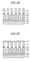
- FIGS. 3A to 3F describe cross-sectional views of an electric field emission device having a triode structure fabricated by using an anodic oxidation process in accordance with a second preferred embodiment of the present invention.
- the second embodiment of the present invention has the same configuration as the first embodiment of the present invention, which is shown in FIGS. 2A to 2F , except that there is formed an anode insulating layer 211 in stead of the alumina layer 212 .
- a bottom electrode layer 202 , a resistive layer 204 and a gate insulating layer 206 are formed on a supporting substrate 200 .
- the resistive layer 204 has been described to be formed between the gate insulating layer 206 and the bottom electrode layer 202 , the formation of the resistive layer 204 may be omitted.
- a gate electrode layer 208 , an anode insulating layer 211 and an aluminum layer 210 are sequentially formed.
- the anode insulating layer 211 is formed by performing one of electron beam deposition, thermal deposition, sputtering, LPCVD (low pressure chemical vapor deposition), sol-gel composition, electroplating and electroless plating techniques.
- the anode insulating layer 211 may contain SiO 2 or metallic oxide and is preferably about 500 nm in thickness. Further, in etching the anode insulating layer 211 , there may be employed one of ion milling, dry etching, wet etching and anodic oxidation techniques.
- the aluminum layer 210 is processed by using an anodic oxidation process to become an alumina layer 212 having sub-micro holes 213 therein.
- a barrier layer 214 of the alumina layer 212 , the anode insulating layer 211 and the gate electrode layer 208 is dry-etched.
- the gate insulating layer 206 is etched to have sub-micro holes therein connecting to the corresponding holes of the alumina layer 212 .
- the alumina layer 212 is removed and then emitters 218 are formed in the holes of the gate insulating layer 206 .
- the process of removing the alumina layer 212 may be carried out by dipping the alumina layer 212 in a solution of phosphoric acid or a mixed solution of phosphoric acid and chromic acid.
- a top electrode layer 220 is formed on the structure as shown in FIG. 3E .
- the top electrode layer 220 is used as an anode of the electric field emission device and also hermetically seals the triode structure fabricated as shown in FIG. 3E .
Landscapes
- Engineering & Computer Science (AREA)
- Manufacturing & Machinery (AREA)
- Cold Cathode And The Manufacture (AREA)
- Cathode-Ray Tubes And Fluorescent Screens For Display (AREA)
Abstract
An electric field emission device having a triode structure is fabricated by using an anodic oxidation process. The device includes a supporting substrate, a bottom electrode layer to be used as an cathode electrode of the device, a gate insulating layer having a plurality of first sub-micro holes, a gate electrode layer having a plurality of second sub-micro holes connecting to the first sub-micro holes, an anode insulating layer having a plurality of third sub-micro holes connecting to the second sub-micro holes, a top electrode layer for hermetically sealing the device, the top electrode layer being used as an anode of the device and a plurality of emitters formed in the first sub-micro holes. The emitters are formed so as to come into as close contact as possible to the electrodes of the device, which results in decreasing a driving voltage.
Description
The present invention relates to an electric field emission device and a method for fabricating same; and, more particularly, to an electric field emission device having a triode structure fabricated by using an anodic oxidation process and a method for fabricating same.
In general, an electric field emission device means a device where electrons are emitted from a surface of metal or semiconductor in a vacuum in accordance with tunneling effect caused by applying electronic field having high intensity to the surface. Such an electric field emission device may be utilized as a high-speed switching device, a microwave generator, an amplifier or a display device. In the device, the emitted electrons can induce high power at a high frequency in a vacuum with low energy loss. Further, the device has several advantages that it has a shorter response time than a conventional solid-state device and may be integrated on a single silicon chip.
Referring to FIG. 1 , the electric field emission device is fabricated as follows. That is, on a glass or a silicon substrate 100, a cathode layer 102, a resistive layer 104, an insulating layer 106 and a gate electrode layer 108 are formed sequentially. And then, photosensitive film patterns, each having a diameter of micrometer, are formed on the gate electrode 108 by using a photolithographic process. Thereafter, the insulating layer 106 is etched by using a reactive ion etching technique such that a surface of the resistive layer 104 is exposed. Subsequently, a metal electric field emission tip 110 containing material such as Mo, W and Cr is vertically deposited on the resistive layer 104 to have a conical shape by using an electron beam evaporation technique.
As mentioned above, the Spindt type electric field emission device has advantages that it has a shorter response time than a conventional solid-state device and may be integrated on a single silicon chip. However, it is difficult to arrange a plurality of micro holes at regular intervals on the electric field emission device as shown in FIG. 1 , particularly when an area of the surface of the device is large. Further, since a distance between an electric field emission tip and an anode electrode is several hundreds micrometers, the electric field emission device as shown in FIG. 1 has a disadvantage that it requires a high driving voltage. Furthermore, there may be needed an additional process to form micro holes, each having a sub-micrometer diameter, on the surface of the gate electrode layer 108.
It is, therefore, an object of the present invention to provide an electric field emission device having a triode structure wherein an array of gate holes, each having a sub-micrometer diameter, are formed thereon by using an anodic oxidation process, to thereby facilitate an arrangement of the gate holes at regular intervals even on a large area, and emitter tips are formed to get a close contact to electrodes, to thereby decrease a driving voltage for the device.
In accordance with one aspect of the present invention, there is provided an electric field emission device having a triode structure fabricated by using an anodic oxidation process, comprising: a supporting substrate; a bottom electrode layer formed on the supporting substrate, which is used as an cathode electrode of the device; a gate insulating layer formed on the bottom electrode layer, having a plurality of first sub-micro holes to be used as gate holes of the device; a gate electrode layer formed on the gate insulating layer, having a plurality of second sub-micro holes each connecting to a corresponding one of the first sub-micro holes; an alumina layer formed on the gate electrode layer, having a plurality of third sub-micro holes each connecting to a corresponding one of the second sub-micro holes; a top electrode layer for hermetically sealing the device in a vacuum, which is formed on the alumina layer and used as an anode of the device; and a plurality of emitters for emitting electrons in a high electric field, each of the emitters being formed in a corresponding one of the first sub-micro holes.
In accordance with another aspect of the present invention, there is provided an electric field emission device having a triode structure fabricated by using an anodic oxidation process, comprising: a supporting substrate; a bottom electrode layer formed on the supporting substrate, which is used as an cathode electrode of the device; a gate insulating layer formed on the bottom electrode layer, having a plurality of first sub-micro holes to be used as gate holes of the device; a gate electrode layer formed on the gate insulating layer, the gate electrode layer having a plurality of second sub-micro holes each connecting to a corresponding one of the first sub-micro holes; an anode insulating layer formed on the gate electrode layer, having a plurality of third sub-micro holes each connecting to a corresponding one of the second sub-micro holes; a top electrode layer for hermetically sealing the device in a vacuum, which is formed on the anode insulating layer and used as an anode of the device; and a plurality of emitters for emitting electrons in a high electric field, each of the emitters being formed in a corresponding one of the first sub-micro holes.
In accordance with still another aspect of the present invention, there is provided a method for fabricating an electric field emission device having a triode structure by using an anodic oxidation process, comprising the steps of: (a) forming a bottom electrode layer on a supporting substrate, the bottom electrode layer being used as an cathode electrode of the device; (b) forming sequentially a gate insulating layer, a gate electrode layer and an aluminum layer on the bottom electrode layer; (c) forming a plurality of first sub-micro holes in an alumina layer by performing an anodic oxidation process on the aluminum layer, thereby transforming the aluminum layer into the alumina layer; (d) etching a barrier layer of the alumina layer and the gate electrode layer, thereby a surface of the gate insulating layer being exposed through the first sub-micro holes; (e) forming a plurality of second sub-micro holes in the gate insulating layer, thereby each of the first sub-micro holes connecting to a corresponding one of the second sub-micro holes; (f) forming an emitter for emitting electron in a high electric field in each of the second sub-micro holes; and (g) forming a top electrode layer for hermetically sealing the device on the alumina layer in a vacuum, the top electrode layer being used as an anode of the device.
In accordance with still another aspect of the present invention, there is provided a method for fabricating an electric field emission device having a triode structure by using an anodic oxidation process, comprising the steps of: (a) forming a bottom electrode layer on a supporting substrate, the bottom electrode layer being used as an cathode electrode of the device; (b) forming sequentially a gate insulating layer, a gate electrode layer, an anode insulating layer and an aluminum layer on the bottom electrode layer; (c) forming a plurality of first sub-micro holes in an alumina layer by performing an anodic oxidation process on the aluminum layer, thereby transforming the aluminum layer into the alumina layer; (d) etching an barrier layer of the alumina layer, the anode insulating layer and the gate electrode layer, thereby a surface of the gate insulating layer being exposed through the first sub-micro holes; (e) forming a plurality of second sub-micro holes in the gate insulating layer, thereby each of the first sub-micro holes connecting to a corresponding one of the second sub-micro holes; (f) removing the alumina layer; (g) forming an emitter for emitting electron in a high electric field in each of the second sub-micro holes; and (h) forming a top electrode layer for hermetically sealing the device on the anode insulating layer in a vacuum, the top electrode layer being used as an anode of the device.
The above and other objects and features of the present invention will become apparent from the following description of preferred embodiments, given in conjunction with the accompanying drawings, in which:
First, as shown in FIG. 2A , the bottom electrode layer 202 containing, e.g., W, Cr, Nb, Al, Ti or alloy thereof is formed on the supporting substrate 200 containing non-conducting material such as glass, e.g., by using a sputtering method or an electron beam deposition method. Instead of the above-mentioned metal, the bottom electrode layer 202 may contain conductive polymer substance, metallic oxide, metallic nitride or metallic sulfide. The thickness of the bottom electrode layer 202 is preferably about 2000 Å.
Thereafter, the resistive layer 204 and the gate insulating layer 206 are sequentially formed on the bottom electrode layer 202 by using the LPCVD method or a reactive sputtering method. Herein, the resistive layer 204 and the gate insulating layer 206 may contain SiO2 or metallic oxide. Further, the thickness of the resistive layer 204 preferably ranges about from 10 Å to several tens Å.
In the meantime, although the resistive layer 204 has been described to be formed between the gate insulating layer 206 and the bottom electrode layer 202, the formation of the resistive layer 204 may be omitted.
Then, on the gate insulating layer 206, the gate electrode layer 208 containing one of Au, W, Nb, Cr, Al and Ti and the aluminum layer 210 are sequentially formed by using a sputtering method. Instead of the above-mentioned metal, the gate electrode layer 208 may contain conductive polymer material, metallic oxide, metallic nitride and metallic sulfide. The thickness of each of the gate insulating layer 206 and the aluminum layer 210 is preferably about 500 nm.
Next, as shown in FIG. 2B , the aluminum layer 210 is processed by using an anodic oxidation process to become an alumina layer 212 having sub-micro holes 213 therein. The anodic oxidation process is performed as follows. That is, a surface of the aluminum layer 210 is polished by using an electropolishing method. The aluminum layer 210 is then dipped in a solution of phosphoric acid, oxalic acid, chromic acid or sulfuric acid and a DC voltage ranging about from 10 V to 200 V is applied thereto, thereby forming the alumina layer 212 having the sub-micro holes 213 therein. In particular, it is preferable to apply a DC voltage of 25 V, 40 V or 195 V to the aluminum layer 210 in order to form the sub-micro holes in the form of a honeycomb.
Subsequently, as shown in FIG. 2C , the barrier layer 214 of the alumina layer 212 and the gate electrode layer 208 is dry-etched by using a reactive ion etching method in an atmosphere of a gas mixture of CF4 and O2, such that a surface of the gate insulating layer 206 is exposed. Alternatively, the barrier layer 214 of alumina layer 212 and the gate electrode layer 208 may be etched by using ion milling or wet etching techniques.
Then, as illustrated in FIG. 2D , the gate insulating layer 206 is etched to have sub-micro holes therein connecting to the corresponding holes of the alumina layer 212. In etching the gate insulating layer 206, there may be employed one of ion milling, dry etching, wet etching and anodic oxidation techniques. Each of thus formed sub-micro holes preferably has a depth ranging about from 500 nm to 1 μm.
Thereafter, as shown in FIG. 2E , emitters 218 are formed in the holes of the gate insulating layer 206. The emitters 218 may be formed by growing metal from bottoms of the holes or by attaching metal to bottoms of the holes. In this case, the emitters 218 is preferably formed to come into as close contact as possible to the gate electrode layer 208, which results in decreasing a driving voltage for the electric field emission device of the present invention.
The growth of the metal in the holes is performed by applying DC or AC voltage (or current) or voltage (or current) pulse to the structure (e.g., the bottom electrode layer 202) shown in FIG. 2D in a solution of metal sulfate, metal nitrate or metal chloride. The height of the growing metal depends on a time period of applying the voltage. Further, the process of growing the metal may be carried out after chemically activating surfaces of the bottoms of the holes. Herein, the metal used in forming the emitters 218 may contain, e.g., Au, Pt, Ni, Mo, W, Ta, Cr, Ti, Co, Cs, Ba, Hf, Nb, Fe, Rb or alloy thereof.
On the other hand, the emitters 218 may be formed by using a carbon nano-structure such as a carbon nano-tube, a carbon nano-fiber, a carbon nano-particle and an amorphous carbon material. Particularly, it is preferable that the carbon nano-tube is used as the emitters 218 since it has such desirable characteristics as high mechanical solidity, high chemical stability and high field enhancement factor.
In the first embodiment of the present invention, the carbon nano-tubes to be used as the emitters 218 may be formed by decomposing thermally or in plazma a gas mixture of hydrocarbon, carbon monoxide, hydrogen and so on at about 200-800° C.
Alternatively, the emitters 218 may be grown in the holes, e.g., by thiolizing a pre-synthesized carbon nano-tube and applying thereto an Au-S chemical composition process. That is, the pre-systhesized carbon nano-tube is dipped into an acid solution and then into a solution containing a group including sulfur, such that a functional group containing sulfur (S) is attached to the carbon nano-tube. Then, the sulfur (S) attached to the carbon nano-tube is coupled to gold formed on a surface of the bottoms of the holes.
The process of growing the carbon nano-tube may utilize the above-described metal growing process to form catalytic metal on the surface of the bottoms of the holes. In this case, the catalytic metal is used to crack a hydrocarbon gas. Otherwise, the emitters may be formed by performing an electrodephoresis process on a pre-synthesized carbon nano-structure.
Although, in this embodiment, only one emitter 218 is formed in each of the holes of the gate insulating layer 206, more than one emitter 218 may be formed in each of the holes. Further, the emitters 218 may be composed by using semiconductor material such as GaN, TiO2 and CdS.
Finally, as shown in FIG. 2F , a top electrode layer 220 is formed on the structure shown in FIG. 2E . The top electrode layer 220 is used as an anode of the electric field emission device and also hermetically seals the triode structure fabricated as shown in FIG. 2E .
The top electrode layer 220 may be formed by depositing metal in a vacuum by employing one of electron beam deposition, thermal deposition, sputtering, LPCVD (low pressure chemical vapor deposition), sol-gel composition, electroplating and electroless plating techniques. The metal used in forming the top electrode layer 220 may be, e.g., Ti, Nb, Mo or Ta, which is generally used as a getter. Otherwise, the top electrode layer 220 may contain one of Al, Ba, V, Zr, Cr, W, conductive polymer material, metallic oxide, metallic nitride and metallic sulfide. Further, the thickness of the top electrode layer 220 preferably ranges about from 300 nm to 1 μm.
In the meantime, FIGS. 3A to 3F describe cross-sectional views of an electric field emission device having a triode structure fabricated by using an anodic oxidation process in accordance with a second preferred embodiment of the present invention.
The second embodiment of the present invention has the same configuration as the first embodiment of the present invention, which is shown in FIGS. 2A to 2F , except that there is formed an anode insulating layer 211 in stead of the alumina layer 212.
In the following, a process of fabricating the electric field emission device in accordance with the second embodiment of the present invention will be described in detail.
First, as shown in FIG. 3A , a bottom electrode layer 202, a resistive layer 204 and a gate insulating layer 206 are formed on a supporting substrate 200. Although the resistive layer 204 has been described to be formed between the gate insulating layer 206 and the bottom electrode layer 202, the formation of the resistive layer 204 may be omitted. Then, on the gate insulating layer 206, a gate electrode layer 208, an anode insulating layer 211 and an aluminum layer 210 are sequentially formed.
Herein, processes of forming the above-mentioned layers and material contained therein are the same as those described with reference to FIG. 2A except those for the anode insulating layer 211. The anode insulating layer 211 is formed by performing one of electron beam deposition, thermal deposition, sputtering, LPCVD (low pressure chemical vapor deposition), sol-gel composition, electroplating and electroless plating techniques. The anode insulating layer 211 may contain SiO2 or metallic oxide and is preferably about 500 nm in thickness. Further, in etching the anode insulating layer 211, there may be employed one of ion milling, dry etching, wet etching and anodic oxidation techniques.
Next, as shown in FIG. 3B , the aluminum layer 210 is processed by using an anodic oxidation process to become an alumina layer 212 having sub-micro holes 213 therein.
Subsequently, as shown in FIG. 3C , a barrier layer 214 of the alumina layer 212, the anode insulating layer 211 and the gate electrode layer 208 is dry-etched. Then, as illustrated in FIG. 3D , the gate insulating layer 206 is etched to have sub-micro holes therein connecting to the corresponding holes of the alumina layer 212.
Thereafter, as shown in FIG. 3E , the alumina layer 212 is removed and then emitters 218 are formed in the holes of the gate insulating layer 206. The process of removing the alumina layer 212 may be carried out by dipping the alumina layer 212 in a solution of phosphoric acid or a mixed solution of phosphoric acid and chromic acid.
Finally, as shown in FIG. 3F , a top electrode layer 220 is formed on the structure as shown in FIG. 3E . The top electrode layer 220 is used as an anode of the electric field emission device and also hermetically seals the triode structure fabricated as shown in FIG. 3E .
Even though the detailed descriptions on material contained in the layers, the processes of fabricating the layers and the dimensions of the layers are not given in the above with reference to FIGS. 3A to 3F , throughout the several views in the accompanying drawings, like reference numerals designate corresponding parts and thus the descriptions given with reference to FIGS. 2A to 2F are also applicable to the corresponding parts shown in FIGS. 3A to 3F.
While the invention has been shown and described with respect to the preferred embodiments, it will be understood by those skilled in the art that various changes and modifications may be made without departing from the spirit and scope of the invention as defined in the following claims.
Claims (39)
1. An electric field emission device having a triode structure fabricated by using an anodic oxidation process, comprising:
a supporting substrate;
a bottom electrode layer formed on the supporting substrate, which is used as a cathode electrode of the device;
a gate insulating layer formed on the bottom electrode layer, the gate insulating layer having a plurality of first sub-micro holes to be used as gate holes of the device;
a gate electrode layer formed on the gate insulating layer, the gate electrode layer having a plurality of second sub-micro holes each connecting to a corresponding one of the first sub-micro holes;
an alumina layer formed on the gate electrode layer, the alumina layer having a plurality of third sub-micro holes each connecting to a corresponding one of the second sub-micro holes, wherein the alumina layer and the plurality of third sub-micro holes are formed by the anodic oxidation process;
a top electrode layer for hermetically sealing the device in a vacuum, which is formed on the alumina layer and used as an anode of the device, wherein the top electrode layer is formed by depositing metal in a vacuum by employing one of electron beam deposition, thermal deposition, sputtering, low pressure chemical vapor deposition, sol-gel composition, electroplating and electoless plating; and
a plurality of emitters for emitting electrons in a high electric field, each of the emitters being formed in a corresponding one of the first sub-micro holes.
2. The device of claim 1 , wherein the emitter contains metal, semiconductor or carbon material.
3. The device of claim 2 , wherein the carbon material is selected from a group consisting of a carbon nano-fiber, a carbon nano-tube, a carbon nano-particle and amorphous carbon material.
4. The device of claim 1 , further comprising a resistive layer formed between the bottom electrode layer and the gate insulating layer.
5. The device of claim 4 , wherein, the resistive layer contains SiO2 or metallic oxide.
6. An electric field emission device having a triode structure fabricated by using an anodic oxidation process, comprising:
a supporting substrate;
a bottom electrode layer formed on the supporting substrate, which is used as a cathode electrode of the device;
a gate insulating layer formed on the bottom electrode layer, having a plurality of first sub-micro holes to be used as gate holes of the device;
a gate electrode layer formed on the gate insulating layer, the gate electrode layer having a plurality of second sub-micro holes each connecting to a corresponding one of the first sub-micro holes;
an anode insulating layer formed on the gate electrode layer, having a plurality of third sub-micro holes each connecting to a corresponding one of the second sub-micro holes, wherein the anode insulating layer is formed by performing one of electron beam deposition, thermal deposition, sputtering, low pressure chemical vapor deposition, sol-gel composition, electroplating and electroless plating;
a top electrode layer for hermetically sealing the device in a vacuum, which is formed on the anode insulating layer and used as an anode of the device, wherein the top electrode layer is formed by depositing metal in a vacuum by employing one of electron beam deposition, thermal deposition, sputtering, low pressure chemical vapor deposition, sol-gel composition, electroplating and electoless plating; and
a plurality of emitters for emitting electrons in a high electric field, each of the emitters being formed in a corresponding one of the first sub-micro holes.
7. The device of claim 6 , wherein the emitter contains metal, semiconductor or carbon material.
8. The device of claim 7 , wherein the carbon material is selected from a group consisting a carbon nano-fiber, a carbon nano-tube, a carbon nano-particle and amorphous carbon material.
9. The device of claim 6 , further comprising a resistive layer formed between the bottom electrode layer and the gate insulating layer.
10. The device of claim 9 , wherein the resistive layer contains SiO2 or metallic oxide.
11. A method for fabricating an electric field emission device having a triode structure by using an anodic oxidation process, comprising the steps of:
(a) forming a bottom electrode layer on a supporting substrate, the bottom electrode layer being used as a cathode electrode of the device;
(b) forming sequentially a gate insulating layer, a gate electrode layer and an aluminum layer on the bottom electrode layer;
(c) forming a plurality of first sub-micro holes in an alumina layer by performing an anodic oxidation process on the aluminum layer, thereby transforming the aluminum layer into the alumina layer;
(d) etching a barrier layer of the alumina layer and the gate electrode layer, thereby a surface of the gate insulating layer being exposed through the first sub-micro holes;
(e) forming a plurality of second sub-micro holes in the gate insulating layer, thereby each of the first sub-micro holes connecting to a corresponding one of the second sub-micro holes;
(f) forming an emitter for emitting electron in a high electric field in each of the second sub-micro holes; and
(g) forming a top electrode layer for hermetically sealing the device on the alumina layer in a vacuum, the top electrode layer being used as an anode of the device.
12. The method of claim 11 , wherein, in the step (c), the anodic oxidation process is performed by using an electrolyte selected from a group consisting of oxalic acid, sulfuric acid, phosphoric acid and chromic acid.
13. The method of claim 11 , wherein, in the step (d), the barrier layer of the alumina layer and the gate electrode layer are etched by using one of ion milling, dry etching and wet etching techniques.
14. The method of claim 11 , wherein, in the step (e), the gate insulating layer is etched by using one of ion milling, dry etching, wet etching and anodic oxidation techniques.
15. The method of claim 11 , wherein, in the step (f), each of the emitters is formed by growing metal from a bottom of each of the second sub-micro holes.
16. The method of claim 15 , wherein the metal is grown by applying DC or AC voltage (or current) or voltage (or current) pulse to a solution of metal sulfate, metal nitrate or metal chloride.
17. The method of claim 15 , wherein the metal is grown by using a solution of metal sulfate, metal nitrate or metal chloride after chemically activating a surface of the bottom.
18. The method of claim 11 , wherein, in the step (f), each of the emitters is formed by attaching metal to a bottom of each of the second sub-micro holes.
19. The method of claim 11 , wherein, in the step (f), each of the emitters is formed by forming a carbon nano-structure on a bottom of each of the second sub-micro holes.
20. The method of claim 19 , wherein the carbon nano-structure is one of carbon nano-tube, carbon nano-fiber, amorphous carbon and carbon nano-particle, which are composed by using a thermal decomposition.
21. The method of claim 20 , wherein the thermal decomposition is performed by thermally decomposing a gas mixture of hydrocarbon, carbon monoxide and hydrogen at 200-800° C.
22. The method of claim 19 , wherein the carbon nano-structure is one of carbon nano-tube, carbon nano-fiber, amorphous carbon and carbon nano-particle, which are composed by using a plasma decomposition.
23. The method of claim 11 , wherein, in the step (f), each of the emitters is formed by thiolizing a pre-synthesized carbon nano-tube and applying thereto an Au-S chemical composition process.
24. The method of claim 11 , wherein, in the step (f), each of the emitters is formed by performing an electrodephoresis process on a pre-synthesized carbon nano-structure.
25. The method of claim 11 , wherein, in the step (f), more than one emitter is formed in each of the second sub-micro holes.
26. A method for fabricating an electric field emission device having a triode structure by using an anodic oxidation process, comprising the steps of:
(a) forming a bottom electrode layer on a supporting substrate, the bottom electrode layer being used as a cathode electrode of the device;
(b) forming sequentially a gate insulating layer, a gate electrode layer, an anode insulating layer and an aluminum layer on the bottom electrode layer;
(c) forming a plurality of first sub-micro holes in an alumina layer by performing an anodic oxidation process on the aluminum layer, thereby transforming the aluminum layer into the alumina layer;
(d) etching an barrier layer of the alumina layer, the anode insulating layer and the gate electrode layer, thereby a surface of the gate insulating layer being exposed through the first sub-micro holes;
(e) forming a plurality of second sub-micro holes in the gate insulating layer, thereby each of the first sub-micro holes connecting to a corresponding one of the second sub-micro holes;
(f) removing the alumina layer;
(g) forming an emitter for emitting electron in a high electric field in each of the second sub-micro holes; and
(h) forming a top electrode layer for hermetically sealing the device on the anode insulating layer in a vacuum, the top electrode layer being used as an anode of the device.
27. The method of claim 26 , wherein, in the step (c), the anodic oxidation process is performed by using an electrolyte selected from a group consisting of oxalic acid, sulfuric acid, phosphoric acid and chromic acid.
28. The method of claim 26 , wherein, in the step (f), the alumina layer is removed by dipping the alumina layer in a solution of phosphoric acid or a mixed solution of phosphoric acid and chromic acid.
29. The method of claim 26 , wherein, in the step (g), each of the emitters is formed by growing metal from a bottom of each of the second sub-micro holes.
30. The method of claim 29 , wherein the metal is grown by applying DC or AC voltage (or current) or voltage (or current) pulse to a solution of metal sulfate, metal nitrate or metal chloride.
31. The method of claim 29 , wherein the metal is grown by using a solution of metal sulfate, metal nitrate or metal chloride after chemically activating a surface of the bottom.
32. The method of claim 26 , wherein, in the step (g), each of the emitters is formed by attaching metal to a bottom of each of the second sub-micro holes.
33. The method of claim 26 , wherein, in the step (g), each of the emitters is formed by forming a carbon nano-structure on a bottom of each of the second sub-micro holes.
34. The method of claim 33 , wherein the carbon nano-structure is one of carbon nano-tube, carbon nano-fiber, amorphous carbon and carbon nano-particle, which are composed by using a thermal decomposition.
35. The method of claim 34 , wherein the thermal decomposition is performed by thermally decomposing a gas mixture of hydrocarbon, carbon monoxide and hydrogen at 200-800° C.
36. The method of claim 33 , wherein the carbon nano-structure is one of carbon nano-tube, carbon nano-fiber, amorphous carbon and carbon nano-particle, which are composed by using a plasma decomposition.
37. The method of claim 26 , wherein, in the step (g), each of the emitters is formed by thiolizing a pre-synthesized carbon nano-tube and applying thereto an Au-S chemical composition process.
38. The method of claim 26 , wherein, in the step (g), each of the emitters is formed by performing an electrodephoresis process on a pre-synthesized carbon nano-structure.
39. The method of claim 26 , wherein, in the step (g), more than one emitter is formed in each of the second sub-micro holes.
Applications Claiming Priority (5)
| Application Number | Priority Date | Filing Date | Title |
|---|---|---|---|
| KR20020044921 | 2002-07-30 | ||
| KR10-2002-0044921 | 2002-07-30 | ||
| KR10-2002-0058158A KR100492509B1 (en) | 2002-07-30 | 2002-09-25 | An electric field emission element having an integrated triode structure which is fabricated by using anodic oxidation process and fabricating method thereof |
| KR10-2002-0058158 | 2002-09-25 | ||
| PCT/KR2003/001526 WO2004012218A1 (en) | 2002-07-30 | 2003-07-30 | Electric field emission device having a triode structure fabricated by using an anodic oxidation process and method for fabricating same |
Publications (2)
| Publication Number | Publication Date |
|---|---|
| US20050285502A1 US20050285502A1 (en) | 2005-12-29 |
| US7554255B2 true US7554255B2 (en) | 2009-06-30 |
Family
ID=31190423
Family Applications (1)
| Application Number | Title | Priority Date | Filing Date |
|---|---|---|---|
| US10/522,572 Expired - Fee Related US7554255B2 (en) | 2002-07-30 | 2003-07-30 | Electric field emission device having a triode structure fabricated by using an anodic oxidation process and method for fabricating same |
Country Status (5)
| Country | Link |
|---|---|
| US (1) | US7554255B2 (en) |
| JP (1) | JP2005535075A (en) |
| CN (1) | CN100541700C (en) |
| AU (1) | AU2003256094A1 (en) |
| WO (1) | WO2004012218A1 (en) |
Families Citing this family (11)
| Publication number | Priority date | Publication date | Assignee | Title |
|---|---|---|---|---|
| KR100576733B1 (en) * | 2003-01-15 | 2006-05-03 | 학교법인 포항공과대학교 | Field emission display having integrated triode structure and method for manufacturing the same |
| US7239076B2 (en) | 2003-09-25 | 2007-07-03 | General Electric Company | Self-aligned gated rod field emission device and associated method of fabrication |
| US20060192494A1 (en) * | 2005-02-25 | 2006-08-31 | Mastroianni Sal T | In-situ sealed carbon nanotube vacuum device |
| US7279085B2 (en) | 2005-07-19 | 2007-10-09 | General Electric Company | Gated nanorod field emitter structures and associated methods of fabrication |
| US7326328B2 (en) | 2005-07-19 | 2008-02-05 | General Electric Company | Gated nanorod field emitter structures and associated methods of fabrication |
| US7485024B2 (en) * | 2005-10-12 | 2009-02-03 | Chunghwa Picture Tubes, Ltd. | Fabricating method of field emission triodes |
| CN1988100B (en) * | 2005-12-20 | 2010-09-29 | 鸿富锦精密工业(深圳)有限公司 | A kind of preparation method of field emission cathode |
| CN103130207B (en) * | 2011-11-22 | 2014-11-12 | 中国科学院合肥物质科学研究院 | Carbon nanometer dropper and preparation method thereof |
| CN112882351A (en) * | 2021-01-20 | 2021-06-01 | 桂林理工大学 | Patterned emitter for electron beam projection lithography system and method of making the same |
| CN113529150B (en) * | 2021-06-23 | 2022-03-29 | 华南理工大学 | A kind of submicron alumina tube and its preparation method and application |
| CN115424909B (en) * | 2022-08-02 | 2025-07-25 | 中国科学院苏州纳米技术与纳米仿生研究所 | Field emission device and manufacturing method thereof |
Citations (25)
| Publication number | Priority date | Publication date | Assignee | Title |
|---|---|---|---|---|
| WO1992000203A1 (en) | 1990-06-28 | 1992-01-09 | Zahnradfabrik Friedrichshafen Ag | Hydropneumatic vehicle suspension |
| US5397957A (en) * | 1990-07-18 | 1995-03-14 | International Business Machines Corporation | Process and structure of an integrated vacuum microelectronic device |
| US5866434A (en) | 1994-12-08 | 1999-02-02 | Meso Scale Technology | Graphitic nanotubes in luminescence assays |
| US5872422A (en) * | 1995-12-20 | 1999-02-16 | Advanced Technology Materials, Inc. | Carbon fiber-based field emission devices |
| JP2000086216A (en) | 1998-09-09 | 2000-03-28 | Toshiba Corp | Method for producing carbon nanotube, field emission type cold cathode device and method for producing the same |
| WO2000017101A1 (en) | 1998-09-18 | 2000-03-30 | William Marsh Rice University | Chemical derivatization of single-wall carbon nanotubes to facilitate solvation thereof; and use of derivatized nanotubes |
| JP2000243247A (en) | 1999-02-19 | 2000-09-08 | Canon Inc | Method for manufacturing electron-emitting device |
| US6203814B1 (en) | 1994-12-08 | 2001-03-20 | Hyperion Catalysis International, Inc. | Method of making functionalized nanotubes |
| WO2001030694A1 (en) | 1999-10-27 | 2001-05-03 | William Marsh Rice University | Macroscopic ordered assembly of carbon nanotubes |
| KR20010058663A (en) | 1999-12-30 | 2001-07-06 | 김순택 | Field emitter array using carbon nanotube and Manufacturing method thereof |
| KR20010068389A (en) | 2000-01-05 | 2001-07-23 | 구자홍 | Field emission display device and its fabrication method |
| JP2002503204A (en) | 1996-03-06 | 2002-01-29 | ハイピリオン カタリシス インターナショナル インコーポレイテッド | Functionalized nanotubes |
| KR20020041665A (en) | 2000-11-28 | 2002-06-03 | 구자홍 | Gate Hole Fabricating Method Thereof, Field Emission Display and Fabricating Method Thereof |
| EP1221710A2 (en) | 2001-01-05 | 2002-07-10 | Samsung SDI Co., Ltd. | Method of manufacturing triode carbon nanotube field emitter array |
| US20020110513A1 (en) | 1998-09-18 | 2002-08-15 | Margrave John L. | Chemical derivatization of single-wall carbon nanotubes to facilitate solvation thereof; and use of derivatized nanotubes to form catalyst-containing seed materials for use in making carbon fibers |
| US6515415B1 (en) * | 2000-02-15 | 2003-02-04 | Samsung Sdi Co., Ltd. | Triode carbon nanotube field emission display using barrier rib structure and manufacturing method thereof |
| US6538367B1 (en) * | 1999-07-15 | 2003-03-25 | Agere Systems Inc. | Field emitting device comprising field-concentrating nanoconductor assembly and method for making the same |
| US20030090190A1 (en) * | 2001-06-14 | 2003-05-15 | Hyperion Catalysis International, Inc. | Field emission devices using modified carbon nanotubes |
| US20030143398A1 (en) | 2000-02-25 | 2003-07-31 | Hiroshi Ohki | Carbon nanotube and method for producing the same, electron source and method for producing the same, and display |
| US6670747B2 (en) | 2000-03-24 | 2003-12-30 | Kabushiki Kaisha Toshiba | Electron source device, method of manufacturing the same, and flat display apparatus comprising an electron source device |
| US6741019B1 (en) * | 1999-10-18 | 2004-05-25 | Agere Systems, Inc. | Article comprising aligned nanowires |
| US6774548B2 (en) * | 2001-08-13 | 2004-08-10 | Delta Optoelectronics, Inc. | Carbon nanotube field emission display |
| US20040202603A1 (en) | 1994-12-08 | 2004-10-14 | Hyperion Catalysis International, Inc. | Functionalized nanotubes |
| US20060049742A1 (en) * | 2003-01-15 | 2006-03-09 | Postech Foundation | Field emission display with integrated triode structure and method for manufacturing the same |
| US7252812B2 (en) | 1998-09-18 | 2007-08-07 | Mary Lou Margrave, legal representative | High-yield method of endohedrally encapsulating species inside fluorinated fullerene nanocages |
Family Cites Families (3)
| Publication number | Priority date | Publication date | Assignee | Title |
|---|---|---|---|---|
| DE69027611T2 (en) * | 1990-07-18 | 1997-01-23 | Ibm | PRODUCTION METHOD AND STRUCTURE OF AN INTEGRATED VACUUM-MICROELECTRONIC DEVICE |
| KR100279737B1 (en) * | 1997-12-19 | 2001-02-01 | 정선종 | Short-wavelength photoelectric device composed of field emission device and optical device and fabrication method thereof |
| JP2000173448A (en) * | 1998-12-09 | 2000-06-23 | Nec Corp | Manufacture of field emission cold cathode |
-
2003
- 2003-07-30 CN CNB038234114A patent/CN100541700C/en not_active Expired - Fee Related
- 2003-07-30 US US10/522,572 patent/US7554255B2/en not_active Expired - Fee Related
- 2003-07-30 JP JP2004524373A patent/JP2005535075A/en active Pending
- 2003-07-30 AU AU2003256094A patent/AU2003256094A1/en not_active Abandoned
- 2003-07-30 WO PCT/KR2003/001526 patent/WO2004012218A1/en not_active Ceased
Patent Citations (38)
| Publication number | Priority date | Publication date | Assignee | Title |
|---|---|---|---|---|
| WO1992000203A1 (en) | 1990-06-28 | 1992-01-09 | Zahnradfabrik Friedrichshafen Ag | Hydropneumatic vehicle suspension |
| US5397957A (en) * | 1990-07-18 | 1995-03-14 | International Business Machines Corporation | Process and structure of an integrated vacuum microelectronic device |
| US6362011B1 (en) | 1994-12-08 | 2002-03-26 | Meso Scale Technologies, Llc | Graphitic nanotubes in luminescence assays |
| US5866434A (en) | 1994-12-08 | 1999-02-02 | Meso Scale Technology | Graphitic nanotubes in luminescence assays |
| US20040202603A1 (en) | 1994-12-08 | 2004-10-14 | Hyperion Catalysis International, Inc. | Functionalized nanotubes |
| US7052861B2 (en) | 1994-12-08 | 2006-05-30 | Meso Scale Technologies, Llc. | Graphitic nanotubes in luminescence assays |
| US6203814B1 (en) | 1994-12-08 | 2001-03-20 | Hyperion Catalysis International, Inc. | Method of making functionalized nanotubes |
| US20060193868A1 (en) | 1994-12-08 | 2006-08-31 | Hyperion Catalysis International, Inc. | Functionalized nanotubes |
| US5872422A (en) * | 1995-12-20 | 1999-02-16 | Advanced Technology Materials, Inc. | Carbon fiber-based field emission devices |
| US20060160246A1 (en) | 1996-03-06 | 2006-07-20 | Massey Richard J | Graphitic nanotubes in luminescence assays |
| JP2002503204A (en) | 1996-03-06 | 2002-01-29 | ハイピリオン カタリシス インターナショナル インコーポレイテッド | Functionalized nanotubes |
| JP2000086216A (en) | 1998-09-09 | 2000-03-28 | Toshiba Corp | Method for producing carbon nanotube, field emission type cold cathode device and method for producing the same |
| US20070098621A1 (en) | 1998-09-18 | 2007-05-03 | William Marsh Rice University | Sidewall derivatized carbon nanotubes |
| US6875412B2 (en) | 1998-09-18 | 2005-04-05 | William Marsh Rice University | Chemically modifying single wall carbon nanotubes to facilitate dispersal in solvents |
| US6841139B2 (en) | 1998-09-18 | 2005-01-11 | William Marsh Rice University | Methods of chemically derivatizing single-wall carbon nanotubes |
| US20020110513A1 (en) | 1998-09-18 | 2002-08-15 | Margrave John L. | Chemical derivatization of single-wall carbon nanotubes to facilitate solvation thereof; and use of derivatized nanotubes to form catalyst-containing seed materials for use in making carbon fibers |
| US6835366B1 (en) | 1998-09-18 | 2004-12-28 | William Marsh Rice University | Chemical derivatization of single-wall carbon nanotubes to facilitate solvation thereof, and use of derivatized nanotubes |
| US6827918B2 (en) | 1998-09-18 | 2004-12-07 | William Marsh Rice University | Dispersions and solutions of fluorinated single-wall carbon nanotubes |
| US6645455B2 (en) | 1998-09-18 | 2003-11-11 | William Marsh Rice University | Chemical derivatization of single-wall carbon nanotubes to facilitate solvation thereof; and use of derivatized nanotubes to form catalyst-containing seed materials for use in making carbon fibers |
| WO2000017101A1 (en) | 1998-09-18 | 2000-03-30 | William Marsh Rice University | Chemical derivatization of single-wall carbon nanotubes to facilitate solvation thereof; and use of derivatized nanotubes |
| US7252812B2 (en) | 1998-09-18 | 2007-08-07 | Mary Lou Margrave, legal representative | High-yield method of endohedrally encapsulating species inside fluorinated fullerene nanocages |
| JP2000243247A (en) | 1999-02-19 | 2000-09-08 | Canon Inc | Method for manufacturing electron-emitting device |
| US6538367B1 (en) * | 1999-07-15 | 2003-03-25 | Agere Systems Inc. | Field emitting device comprising field-concentrating nanoconductor assembly and method for making the same |
| US6741019B1 (en) * | 1999-10-18 | 2004-05-25 | Agere Systems, Inc. | Article comprising aligned nanowires |
| US6790425B1 (en) | 1999-10-27 | 2004-09-14 | Wiliam Marsh Rice University | Macroscopic ordered assembly of carbon nanotubes |
| US20050169830A1 (en) | 1999-10-27 | 2005-08-04 | William Marsh Rice University | Macroscopic ordered assembly of carbon nanotubes |
| WO2001030694A1 (en) | 1999-10-27 | 2001-05-03 | William Marsh Rice University | Macroscopic ordered assembly of carbon nanotubes |
| US20080210370A1 (en) | 1999-10-27 | 2008-09-04 | Smalley Richard E | Macroscopic ordered assembly of carbon nanotubes |
| KR20010058663A (en) | 1999-12-30 | 2001-07-06 | 김순택 | Field emitter array using carbon nanotube and Manufacturing method thereof |
| KR20010068389A (en) | 2000-01-05 | 2001-07-23 | 구자홍 | Field emission display device and its fabrication method |
| US6515415B1 (en) * | 2000-02-15 | 2003-02-04 | Samsung Sdi Co., Ltd. | Triode carbon nanotube field emission display using barrier rib structure and manufacturing method thereof |
| US20030143398A1 (en) | 2000-02-25 | 2003-07-31 | Hiroshi Ohki | Carbon nanotube and method for producing the same, electron source and method for producing the same, and display |
| US6670747B2 (en) | 2000-03-24 | 2003-12-30 | Kabushiki Kaisha Toshiba | Electron source device, method of manufacturing the same, and flat display apparatus comprising an electron source device |
| KR20020041665A (en) | 2000-11-28 | 2002-06-03 | 구자홍 | Gate Hole Fabricating Method Thereof, Field Emission Display and Fabricating Method Thereof |
| EP1221710A2 (en) | 2001-01-05 | 2002-07-10 | Samsung SDI Co., Ltd. | Method of manufacturing triode carbon nanotube field emitter array |
| US20030090190A1 (en) * | 2001-06-14 | 2003-05-15 | Hyperion Catalysis International, Inc. | Field emission devices using modified carbon nanotubes |
| US6774548B2 (en) * | 2001-08-13 | 2004-08-10 | Delta Optoelectronics, Inc. | Carbon nanotube field emission display |
| US20060049742A1 (en) * | 2003-01-15 | 2006-03-09 | Postech Foundation | Field emission display with integrated triode structure and method for manufacturing the same |
Non-Patent Citations (1)
| Title |
|---|
| Patent Abstracts of Japan, vol. 00, N 06; Sep. 22, 2000, & JP 2000086216 A (Tokyo Shibaura) Mar. 28, 2000, abstract, Fig. 7 and paragraphs 0049, 0050 of English translation. |
Also Published As
| Publication number | Publication date |
|---|---|
| WO2004012218A1 (en) | 2004-02-05 |
| US20050285502A1 (en) | 2005-12-29 |
| CN1685460A (en) | 2005-10-19 |
| CN100541700C (en) | 2009-09-16 |
| AU2003256094A1 (en) | 2004-02-16 |
| JP2005535075A (en) | 2005-11-17 |
Similar Documents
| Publication | Publication Date | Title |
|---|---|---|
| US7070472B2 (en) | Field emission display and methods of forming a field emission display | |
| JP3902883B2 (en) | Nanostructure and manufacturing method thereof | |
| US20060270229A1 (en) | Anodized aluminum oxide nanoporous template and associated method of fabrication | |
| US6803704B2 (en) | Channel plate and manufacturing method thereof | |
| US6737668B2 (en) | Method of manufacturing structure with pores and structure with pores | |
| KR100695124B1 (en) | Horizontal Growth Method of Carbon Nanotubes | |
| KR960000315B1 (en) | Manufacturing method of metal micro cold cathode | |
| US7554255B2 (en) | Electric field emission device having a triode structure fabricated by using an anodic oxidation process and method for fabricating same | |
| JP3729449B2 (en) | Structure and device having pores | |
| JP2003016921A (en) | Structure, electron-emitting device, image forming apparatus, and manufacturing method thereof | |
| KR100243990B1 (en) | Field emission cathode and method for manufacturing the same | |
| KR19990073592A (en) | Fabrication of carbon nanotube field-emitting device using lift-off process. | |
| JP2005060146A (en) | Carbon thin film and field emission electron source and working electrode using the same | |
| JP2003342791A (en) | Structure having pores and method for producing the same | |
| KR20010029763A (en) | Method for manufacturing field emission display device using carbon nanotube | |
| JPH09270228A (en) | Method of manufacturing field emission electron source | |
| US20070200478A1 (en) | Field Emission Device | |
| KR100492509B1 (en) | An electric field emission element having an integrated triode structure which is fabricated by using anodic oxidation process and fabricating method thereof | |
| Holland et al. | Large area gridded field emitter arrays using anodised aluminium | |
| RU2579777C1 (en) | Device based on carbon-containing cold cathodes arranged on semiconductor substrate, and method of making same | |
| JP4371976B2 (en) | Field electron emission device | |
| KR100767417B1 (en) | Carbon nanotube field emission device and manufacturing method thereof | |
| JP4097224B2 (en) | Nanostructure and electron-emitting device | |
| JP3805228B2 (en) | Method for manufacturing electron-emitting device | |
| KR100322611B1 (en) | Fabrication Method of Field Emission Device Using Carbon Nanotube |
Legal Events
| Date | Code | Title | Description |
|---|---|---|---|
| AS | Assignment |
Owner name: POSTECH FOUNDATION, KOREA, REPUBLIC OF Free format text: ASSIGNMENT OF ASSIGNORS INTEREST;ASSIGNORS:LEE, KUN-HONG;HWANG, SUN-KYU;JEONG, SOO-HWAN;REEL/FRAME:016956/0720 Effective date: 20050120 |
|
| FEPP | Fee payment procedure |
Free format text: PAYOR NUMBER ASSIGNED (ORIGINAL EVENT CODE: ASPN); ENTITY STATUS OF PATENT OWNER: SMALL ENTITY |
|
| FPAY | Fee payment |
Year of fee payment: 4 |
|
| REMI | Maintenance fee reminder mailed | ||
| LAPS | Lapse for failure to pay maintenance fees | ||
| STCH | Information on status: patent discontinuation |
Free format text: PATENT EXPIRED DUE TO NONPAYMENT OF MAINTENANCE FEES UNDER 37 CFR 1.362 |
|
| FP | Lapsed due to failure to pay maintenance fee |
Effective date: 20170630 |