US7514357B2 - Method of manufacturing a semiconductor device - Google Patents
Method of manufacturing a semiconductor device Download PDFInfo
- Publication number
- US7514357B2 US7514357B2 US11/293,693 US29369305A US7514357B2 US 7514357 B2 US7514357 B2 US 7514357B2 US 29369305 A US29369305 A US 29369305A US 7514357 B2 US7514357 B2 US 7514357B2
- Authority
- US
- United States
- Prior art keywords
- etching
- plasma
- trench
- gas
- photoresist
- Prior art date
- Legal status (The legal status is an assumption and is not a legal conclusion. Google has not performed a legal analysis and makes no representation as to the accuracy of the status listed.)
- Expired - Fee Related, expires
Links
Images


Classifications
-
- H10D64/011—
-
- H10W20/081—
-
- H10P50/287—
-
- H10P70/234—
-
- H10W20/084—
Definitions
- the present invention relate to a method of manufacturing a semiconductor device. More particularly, the present invention relates to a method of manufacturing a semiconductor device that removes residues of polymer remaining in a trench for a metal line.
- a semiconductor device has a plurality of layers sequentially formed on a substrate.
- an interlayer insulation layer such as an oxide layer is required for insulation between layers, and a metal line may be formed in each layer.
- metal lines i.e., upper and lower metal lines
- metal lines of adjacent metal layers having an interlayer insulation layer therebetween may be electrically connected with each other through a via hole formed through the interlayer insulation layer.
- a lower metal line is firstly formed, and then a thick interlayer insulation layer is formed thereon.
- a photoresist pattern is formed on the interlayer insulation layer, for example, through a photomask process (application of a photoresist, exposure, development, etc.). Then, a via hole or a trench that selectively exposes an upper surface of the lower metal line may be formed by an etching process using the photoresist pattern.
- a via hole 104 and a trench 106 are formed in a semiconductor substrate 102 (typically using separate photolithography steps for the trench and via).
- the uppermost portion of the semiconductor substrate 102 includes the interlayer insulation layer (such as an oxide layer).
- the photoresist pattern and residues of the etching process for example, a carbon-based polymer
- a dry ashing process for example, an O 2 ashing process
- a solvent cleaning process etc.
- a crown defect formed in the trench may be a cause of degradation of electrical characteristics of a metal material that will be filled in the via hole and the trench. In this case, the reliability and productivity of the semiconductor device may deteriorate.
- the present invention has been made in an effort to provide a method of manufacturing a semiconductor device having advantages of preventing degradation of electrical characteristics of a semiconductor device by fully removing a residue such as a polymer formed in a trench.
- An exemplary method of manufacturing a semiconductor device includes: etching a via hole and a trench in a semiconductor substrate; coating a photoresist on the semiconductor substrate such that the via hole and the trench may be filled thereby; removing a polymer defect in the trench while removing the coated photoresist by a plasma treatment under predetermined process conditions; and performing a wet cleaning process so as to remove a residue of the photoresist.
- the removal of the polymer defect in the trench may include: patterning the photoresist by partially removing the photoresist above the trench; exposing a bottom side of the trench by etching the photoresist; removing the polymer defect in the trench by plasma etching in a first atmosphere under first predetermined process conditions; and removing the photoresist remaining on the semiconductor substrate by plasma etching in a second atmosphere under second predetermined process conditions.
- a critical dimension of the patterned portion of the photoresist may be less than a critical dimension of the trench.
- the critical dimension of the patterned portion of the photoresist may be less than the critical dimension of the trench by at least 15 to 25%.
- the bottom side of the trench may be exposed by etching the photoresist in an O 2 gas atmosphere under a first power condition of 0 W and then under a second power condition of a few hundred to a few thousand W (e.g., 200 to 5000 W). Exposing the bottom side of the trench may comprise a temperature condition of 200 to 250° C.
- the first plasma etching atmosphere may comprise a CF 4 and Ar atmosphere.
- the first plasma etching conditions may comprise a power condition of at least 1000 W.
- the CF 4 and Ar gas volumes may be set at a ratio of about 1:10.
- the second plasma etching atmosphere may comprise a first O 2 plasma atmosphere then an O 3 plasma atmosphere.
- the O 2 plasma etching conditions may comprise sequential plasma etching conditions of about 1 Torr pressure/about 1700 W power/a flow rate of about 2000 sccm O 2 /a temperature of about 250° C., about 1 Torr pressure/about 1700 W power/a flow rate of about 2000 sccm O 2 /a temperature of about 250° C., and about 1 Torr pressure/about 1700 W power/a flow rate of about 2000 sccm O 2 /a temperature of about 250° C.
- the O 3 plasma etching conditions may comprise sequential plasma etching conditions of about 2 Torr pressure/about 0 W power/a flow rate of about 2000 sccm O 3 /a temperature of about 250° C., about 2 Torr pressure/about 2000 W power/a flow rate of about 2000 sccm O 3 /a temperature of about 250° C., and about 500 Torr pressure/about 2500 W power/a flow rate of about 2000 sccm O 3 /a temperature of about 250° C.
- FIG. 1 is a cross-sectional view showing a crown defect as an exemplary defect formed in a trench that is formed on a semiconductor substrate according to a conventional etching process.
- FIG. 2A to FIG. 2E are cross-sectional views showing sequential stages of forming a trench in a semiconductor substrate by an etching process according to an exemplary embodiment of the present invention.
- a photoresist is formed entirely (e.g., blanket deposited) thereon, and then the photoresist is partially removed (e.g., by photolithography and development). Accordingly, a polymer residue (for example, a crown defect) may be exposed. After the exposed polymer residue is removed, the photoresist remaining in the via hole and the trench is removed by a plasma treatment. As a result, the trench may be free from a polymer residue.
- FIG. 2A to FIG. 2E are cross-sectional views showing sequential stages of forming a trench on a semiconductor substrate by an etching process according to an exemplary embodiment of the present invention.
- a photoresist pattern is formed on a semiconductor substrate 202 having one or more interlayer insulation layers (for example, an oxide layer such as silicon dioxide, a boron- and/or phosphorous-doped silicon dioxide, or a fluorosilicate glass [FSG] having one or more undoped silicate glass [USG] and/or silicon nitride layers thereon, thereunder or interposed therethrough) by a photomask process (application of a photoresist, an exposure, development, etc.).
- interlayer insulation layers for example, an oxide layer such as silicon dioxide, a boron- and/or phosphorous-doped silicon dioxide, or a fluorosilicate glass [FSG] having one or more undoped silicate glass [USG] and/or silicon nitride layers thereon, thereunder or interposed therethrough
- a via hole 204 that selectively exposes an upper surface of the lower metal line may be formed by an etching process using the photoresist pattern, followed by forming a trench 206 by etching the interlayer insulation layer(s) 202 using a second photoresist pattern, similarly to formation of via hole 204 , or vice versa.
- a residue such as a polymer produced during etching of the semiconductor substrate 202 may be formed in the trench 206 , and a crown defect 208 (e.g., comprising the polymer) may be formed as shown in FIG. 2A .
- the crown defect 208 of the polymer is not generally removed by ashing and solvent cleaning processes, and it usually remains in the trench 206 after such processes.
- a photoresist is again coated on the substrate after forming the trench 206 (and via 204 ) in order to remove the crown defect 208 of the polymer. Subsequently, the crown defect is exteriorly exposed by ashing the photoresist. Then, the crown defect is removed by another ashing process under predetermined ashing conditions, and the photoresist remaining in the via hole is removed. Finally, a solvent cleaning process (i.e., a wet cleaning process) may be performed.
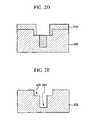
- ashing and solvent cleaning processes are not immediately performed after forming the via hole 204 and the trench 206 in the semiconductor substrate 202 . That is, as shown in FIG. 2B , a photoresist layer 210 is formed on an entire surface of the semiconductor substrate 202 , for example, by a blanket deposition technique such as spin coating, such that the crown defect 208 may be fully covered by the photoresist 210 .
- the photoresist layer 210 may be relatively thick (e.g., about or slightly greater than a conventional photoresist thickness). Subsequently, the photoresist 210 is partially removed by patterning the photoresist 210 (e.g., by selective exposure and development) as shown in FIG. 2B .
- the patterned portion of the photoresist 210 has a critical dimension cd 2 that is smaller than a critical dimension cd 1 of the trench, for example, by about 15 to 25%.
- the patterned portion of the photoresist 210 has a critical dimension cd 2 that is greater than a width of the via 204 (for example, by at least about 15 to 25%).
- sidewalls of the trench 206 may be protected from etching for removing the crown defect 208 through a subsequent ashing process.
- the critical dimension cd 1 of the trench 206 is 0.15 ⁇ m
- the critical dimension cd 2 of the patterned portion of the photoresist 210 may be about 0.12 ⁇ m.
- the crown defect 208 (e.g., comprising a polymer formed during initial trench and via etching) is fully exposed as shown in FIG. 2C , by etching the photoresist 210 on an entire surface thereof (e.g., anisotropic etching) through an ashing process including two ashing steps in an O 2 gas atmosphere under the following process conditions. That is, a bottom surface of the trench 206 is generally fully exposed after an ashing process comprising the following two steps:
- the ashing process is preferably performed under a power condition (e.g., an RF source power) of about 0 W at step 1, and under a power condition (e.g., the RF source power) of about 1500 W at step 2.
- a power condition e.g., an RF source power
- the ashing process is preferably performed under a temperature condition of about 220° C. (in a range of about 200 to 250° C.).
- the power condition at step 2 may be set to be a few hundred to a few thousand W (e.g., from 200 to 5000 W), depending on the type of the photoresist 210 and/or its thickness.
- an etching process in a first plasma atmosphere under the following process conditions may be performed such that the exposed crown defect 208 can be fully removed as shown in FIG. 2D .
- source and bias powers are set to be 1500 W at the above step, the present invention is not necessarily limited thereto.
- the values of the source and bias powers are set so that etching reactivity is stronger at a bottom side than at a lateral side of the trench 206 , and for this purpose, the source and bias powers may both be above 1000 W, with generally about the same values for the other process conditions.
- the volume of the CF 4 gas and the Ar gas may be set at a ratio of about 1:10, although a ratio of from about 1:5 to about 1:20 may be suitable.
- the total flow rate of the fluorocarbon (e.g., CF 4 ) and inert (e.g., Ar) gases may be from 300 to 1500 sccm, and the etching chamber pressure may be from 3 to 100 mTorr (preferably from 20 to 60 mTorr).
- an etching process in a second plasma atmosphere having the following process conditions may be performed to substantially remove the photoresist 210 remaining on top of the semiconductor substrate 202 and in the via hole 204 :
- the etching process in the second plasma atmosphere is realized by consecutively performing O 2 plasma atmosphere etching, then O 3 plasma atmosphere etching.
- the O 2 plasma atmosphere etching may be performed using the above steps 1 to 3
- the O 3 plasma atmosphere etching may be performed using steps 4 to 6.
- each process condition may be varied as follows. That is, the pressure may remain at substantially the same level throughout steps 1 to 3 (although the actual value may vary from about 0.5 mTorr to about 5 mTorr).
- the flow rate of O 2 gas used at step 1 is less than that at step 2, so that step 1 may have a smaller ashing rate.
- a relatively small amount of O 2 gas is used at step 3 (although the actual values may vary from 100 to 4000 sccm).
- the power remains at about the same level throughout steps 1 to 3 (although the actual value may vary from about 1000 to about 2500 W).
- the process time of step 1 may be about 10-20 seconds.
- the process time of step 2 is set to be a time to reach an end point (e.g., as determined by conventional end point detection, or EPD), and the process time of step 3 may be about the same as that of the first or fifth steps (preferably the same as the first step).
- the O 3 gas may be used at a relatively higher pressure that that of O 2 gas in steps 1 to 3 (e.g., from about 1 mTorr to about 10 mTorr for steps 4-5, and from about 100 mTorr to about 1500 mTorr for step 6).
- the power is turned off.
- the pressure at step 6 is relatively high. A relatively high power is used at step 6, considering the possibility of remaining photoresist residue.
- the photoresist pattern 210 remaining on the semiconductor substrate 202 may be fully removed by performing an ashing process comprising the above-described plasma treatment (e.g., step 1 to step 6) under the above-described series of process conditions.
- the photoresist residue may be washed off by a wet cleaning process such as a solvent cleaning, and accordingly, as shown in FIG. 2E , a trench 206 may be completed at a target position of the semiconductor substrate 202 without leaving a defect of a polymer such as a crown defect of the polymer.
- the photoresist pattern has been described to be formed directly on the semiconductor substrate.
- the present invention is not necessarily limited thereto, and the photoresist pattern may be formed after a pad oxide layer (or a buffer oxide layer or antireflective coating) is formed on the semiconductor substrate.
- substantially the same result may be obtained when the post-treatment process (that is, removing a polymer defect formed in the trench) is performed after the formation of the trench.
- a photoresist is coated (e.g., blanket deposited) on an entire surface of a semiconductor substrate after forming a via hole and a trench therein. After exposing a polymer residue by partially removing the photoresist, the exposed polymer residue is removed. Subsequently, the polymer residue is fully removed by a post-treatment process in which the photoresist remaining in the via hole and the trench is removed by a plasma treatment. Consequently, degradation of electric characteristics and deterioration of reliability of a semiconductor device may be effectively reduced or prevented even if a polymer is formed in a trench during an etching process for forming the trench.
Landscapes
- Drying Of Semiconductors (AREA)
- Internal Circuitry In Semiconductor Integrated Circuit Devices (AREA)
Abstract
Description
-
- Step 1: 1 Torr/0 W/2500 sccm O2/30 seconds/220° C.
- Step 2: 1 Torr/1500 W/2500 sccm O2/30 seconds/220° C.
-
- Crown Defect Removal Step: 40 mTorr/1500 W (source)/1500 W (bias)/80 sccm CF4/800 sccm Ar/30 seconds
-
- Step 1: 1 Torr/1700 W/1000 sccm O2/15 seconds/250° C.
- Step 2: 1 Torr/1700 W/2000 sccm O2/30 seconds/250° C.
- Step 3: 1 Torr/1700 W/1000 sccm O2/15 seconds/250° C.
- Step 4: 2 Torr/0 W/2000 sccm O3/20 seconds/250° C.
- Step 5: 2 Torr/2000 W/2000 sccm O3/30 seconds/250° C.
- Step 6: 500 Torr/2500 W/2000 sccm O3/30 seconds/250° C.
Claims (22)
Applications Claiming Priority (2)
| Application Number | Priority Date | Filing Date | Title |
|---|---|---|---|
| KR10-2004-0113659 | 2004-12-28 | ||
| KR1020040113659A KR100641485B1 (en) | 2004-12-28 | 2004-12-28 | Semiconductor device manufacturing method |
Publications (2)
| Publication Number | Publication Date |
|---|---|
| US20060141776A1 US20060141776A1 (en) | 2006-06-29 |
| US7514357B2 true US7514357B2 (en) | 2009-04-07 |
Family
ID=36612289
Family Applications (1)
| Application Number | Title | Priority Date | Filing Date |
|---|---|---|---|
| US11/293,693 Expired - Fee Related US7514357B2 (en) | 2004-12-28 | 2005-12-02 | Method of manufacturing a semiconductor device |
Country Status (2)
| Country | Link |
|---|---|
| US (1) | US7514357B2 (en) |
| KR (1) | KR100641485B1 (en) |
Families Citing this family (2)
| Publication number | Priority date | Publication date | Assignee | Title |
|---|---|---|---|---|
| CN103420329B (en) * | 2013-08-29 | 2016-03-23 | 上海华虹宏力半导体制造有限公司 | For the TaN etch polymers residue removal method of MEMS technology |
| KR102275502B1 (en) | 2015-01-05 | 2021-07-09 | 삼성전자주식회사 | Variable resistance devices and methods of manufacturing the same |
Citations (15)
| Publication number | Priority date | Publication date | Assignee | Title |
|---|---|---|---|---|
| US5543335A (en) * | 1993-05-05 | 1996-08-06 | Ixys Corporation | Advanced power device process for low drop |
| US6277752B1 (en) * | 1999-06-28 | 2001-08-21 | Taiwan Semiconductor Manufacturing Company | Multiple etch method for forming residue free patterned hard mask layer |
| US20030203642A1 (en) * | 1998-11-25 | 2003-10-30 | Smith Patricia B. | Method for photoresist strip, sidewall polymer removal and passivation for aluminum metallization |
| US20040063306A1 (en) * | 2002-09-30 | 2004-04-01 | Koichi Takeuchi | Fabrication method of semiconductor device |
| US6727185B1 (en) * | 1999-11-29 | 2004-04-27 | Texas Instruments Incorporated | Dry process for post oxide etch residue removal |
| US20040157448A1 (en) * | 1999-06-17 | 2004-08-12 | Micron Technology, Inc. | Compositions and methods for removing etch residue |
| US6777344B2 (en) * | 2001-02-12 | 2004-08-17 | Lam Research Corporation | Post-etch photoresist strip with O2 and NH3 for organosilicate glass low-K dielectric etch applications |
| US6833081B2 (en) * | 2001-12-21 | 2004-12-21 | Nanya Technology Corporation | Method of metal etching post cleaning |
| US6884728B2 (en) * | 2002-11-06 | 2005-04-26 | Taiwan Semiconductor Manufacturing Co., Ltd. | Method for removing polymeric residue contamination on semiconductor feature sidewalls |
| US20050106888A1 (en) * | 2003-11-14 | 2005-05-19 | Taiwan Semiconductor Manufacturing Co. | Method of in-situ damage removal - post O2 dry process |
| US6924221B2 (en) * | 2002-12-03 | 2005-08-02 | Taiwan Semiconductor Manufacturing Co., Ltd. | Integrated process flow to improve copper filling in a damascene structure |
| US7112532B2 (en) * | 2001-07-09 | 2006-09-26 | Texas Instruments Incorporated | Process for forming a dual damascene structure |
| US7196002B2 (en) * | 2004-08-09 | 2007-03-27 | Taiwan Semiconductor Manufacturing Co., Ltd. | Method of making dual damascene with via etch through |
| US7199059B2 (en) * | 2004-10-26 | 2007-04-03 | United Microelectronics Corp. | Method for removing polymer as etching residue |
| US7253116B2 (en) * | 2004-11-18 | 2007-08-07 | International Business Machines Corporation | High ion energy and reative species partial pressure plasma ash process |
-
2004
- 2004-12-28 KR KR1020040113659A patent/KR100641485B1/en not_active Expired - Fee Related
-
2005
- 2005-12-02 US US11/293,693 patent/US7514357B2/en not_active Expired - Fee Related
Patent Citations (15)
| Publication number | Priority date | Publication date | Assignee | Title |
|---|---|---|---|---|
| US5543335A (en) * | 1993-05-05 | 1996-08-06 | Ixys Corporation | Advanced power device process for low drop |
| US20030203642A1 (en) * | 1998-11-25 | 2003-10-30 | Smith Patricia B. | Method for photoresist strip, sidewall polymer removal and passivation for aluminum metallization |
| US20040157448A1 (en) * | 1999-06-17 | 2004-08-12 | Micron Technology, Inc. | Compositions and methods for removing etch residue |
| US6277752B1 (en) * | 1999-06-28 | 2001-08-21 | Taiwan Semiconductor Manufacturing Company | Multiple etch method for forming residue free patterned hard mask layer |
| US6727185B1 (en) * | 1999-11-29 | 2004-04-27 | Texas Instruments Incorporated | Dry process for post oxide etch residue removal |
| US6777344B2 (en) * | 2001-02-12 | 2004-08-17 | Lam Research Corporation | Post-etch photoresist strip with O2 and NH3 for organosilicate glass low-K dielectric etch applications |
| US7112532B2 (en) * | 2001-07-09 | 2006-09-26 | Texas Instruments Incorporated | Process for forming a dual damascene structure |
| US6833081B2 (en) * | 2001-12-21 | 2004-12-21 | Nanya Technology Corporation | Method of metal etching post cleaning |
| US20040063306A1 (en) * | 2002-09-30 | 2004-04-01 | Koichi Takeuchi | Fabrication method of semiconductor device |
| US6884728B2 (en) * | 2002-11-06 | 2005-04-26 | Taiwan Semiconductor Manufacturing Co., Ltd. | Method for removing polymeric residue contamination on semiconductor feature sidewalls |
| US6924221B2 (en) * | 2002-12-03 | 2005-08-02 | Taiwan Semiconductor Manufacturing Co., Ltd. | Integrated process flow to improve copper filling in a damascene structure |
| US20050106888A1 (en) * | 2003-11-14 | 2005-05-19 | Taiwan Semiconductor Manufacturing Co. | Method of in-situ damage removal - post O2 dry process |
| US7196002B2 (en) * | 2004-08-09 | 2007-03-27 | Taiwan Semiconductor Manufacturing Co., Ltd. | Method of making dual damascene with via etch through |
| US7199059B2 (en) * | 2004-10-26 | 2007-04-03 | United Microelectronics Corp. | Method for removing polymer as etching residue |
| US7253116B2 (en) * | 2004-11-18 | 2007-08-07 | International Business Machines Corporation | High ion energy and reative species partial pressure plasma ash process |
Also Published As
| Publication number | Publication date |
|---|---|
| KR20060075100A (en) | 2006-07-04 |
| KR100641485B1 (en) | 2006-11-01 |
| US20060141776A1 (en) | 2006-06-29 |
Similar Documents
| Publication | Publication Date | Title |
|---|---|---|
| US20050214694A1 (en) | Pattern formation method | |
| US8017517B2 (en) | Dual damascene process | |
| US20070134917A1 (en) | Partial-via-first dual-damascene process with tri-layer resist approach | |
| US7537998B2 (en) | Method for forming salicide in semiconductor device | |
| JP4108228B2 (en) | Manufacturing method of semiconductor device | |
| US6645864B1 (en) | Physical vapor deposition of an amorphous silicon liner to eliminate resist poisoning | |
| US7371507B2 (en) | Methods for fabricating semiconductor devices | |
| US6511902B1 (en) | Fabrication method for forming rounded corner of contact window and via by two-step light etching technique | |
| US20050142830A1 (en) | Method for forming a contact of a semiconductor device | |
| US7514357B2 (en) | Method of manufacturing a semiconductor device | |
| US6803307B1 (en) | Method of avoiding enlargement of top critical dimension in contact holes using spacers | |
| US20080233490A1 (en) | Mask rework method | |
| US7384823B2 (en) | Method for manufacturing a semiconductor device having a stabilized contact resistance | |
| JPH1167909A (en) | Method for manufacturing semiconductor device | |
| US7148150B2 (en) | Method of forming metal line layer in semiconductor device | |
| US20040121580A1 (en) | Method for fabricating metal line of semiconductor device | |
| KR100278995B1 (en) | Method for forming via hole in semiconductor device | |
| KR100744803B1 (en) | MIM Capacitor Manufacturing Method Of Semiconductor Device | |
| JP3833603B2 (en) | Manufacturing method of semiconductor device | |
| KR100652285B1 (en) | How to remove photoresist residue | |
| KR100458081B1 (en) | Via hole formation method of semiconductor device | |
| KR100687856B1 (en) | Planarization method of semiconductor device | |
| KR20090045717A (en) | Manufacturing Method of Semiconductor Device | |
| KR100744089B1 (en) | Semiconductor device manufacturing method | |
| US20050239285A1 (en) | Damascene process capable of avoiding via resist poisoning |
Legal Events
| Date | Code | Title | Description |
|---|---|---|---|
| AS | Assignment |
Owner name: DONGBUANAM SEMICONDUCTOR INC., KOREA, REPUBLIC OF Free format text: ASSIGNMENT OF ASSIGNORS INTEREST;ASSIGNOR:JO, BO-YEOUN;REEL/FRAME:017334/0207 Effective date: 20051202 |
|
| AS | Assignment |
Owner name: DONGBU ELECTRONICS CO., LTD.,KOREA, REPUBLIC OF Free format text: CHANGE OF NAME;ASSIGNOR:DONGANAM SEMICONDUCTOR INC.;REEL/FRAME:017749/0335 Effective date: 20060328 Owner name: DONGBU ELECTRONICS CO., LTD., KOREA, REPUBLIC OF Free format text: CHANGE OF NAME;ASSIGNOR:DONGANAM SEMICONDUCTOR INC.;REEL/FRAME:017749/0335 Effective date: 20060328 |
|
| AS | Assignment |
Owner name: DONGBU ELECTRONICS CO., LTD., KOREA, REPUBLIC OF Free format text: CORRECTIVE ASSIGNMENT TO CORRECT THE ASSIGNOR PREVIOUSLY RECORDED ON REEL 017749 FRAME 0335;ASSIGNOR:DONGBUANAM SEMICONDUCTOR INC.;REEL/FRAME:017821/0670 Effective date: 20060328 Owner name: DONGBU ELECTRONICS CO., LTD.,KOREA, REPUBLIC OF Free format text: CORRECTIVE ASSIGNMENT TO CORRECT THE ASSIGNOR PREVIOUSLY RECORDED ON REEL 017749 FRAME 0335. ASSIGNOR(S) HEREBY CONFIRMS THE ASSIGNOR SHOULD BE "DONGBUANAM SEMICONDUCTOR INC.";ASSIGNOR:DONGBUANAM SEMICONDUCTOR INC.;REEL/FRAME:017821/0670 Effective date: 20060328 Owner name: DONGBU ELECTRONICS CO., LTD., KOREA, REPUBLIC OF Free format text: CORRECTIVE ASSIGNMENT TO CORRECT THE ASSIGNOR PREVIOUSLY RECORDED ON REEL 017749 FRAME 0335. ASSIGNOR(S) HEREBY CONFIRMS THE ASSIGNOR SHOULD BE "DONGBUANAM SEMICONDUCTOR INC.";ASSIGNOR:DONGBUANAM SEMICONDUCTOR INC.;REEL/FRAME:017821/0670 Effective date: 20060328 |
|
| FEPP | Fee payment procedure |
Free format text: PAYOR NUMBER ASSIGNED (ORIGINAL EVENT CODE: ASPN); ENTITY STATUS OF PATENT OWNER: LARGE ENTITY |
|
| REMI | Maintenance fee reminder mailed | ||
| LAPS | Lapse for failure to pay maintenance fees | ||
| STCH | Information on status: patent discontinuation |
Free format text: PATENT EXPIRED DUE TO NONPAYMENT OF MAINTENANCE FEES UNDER 37 CFR 1.362 |
|
| STCH | Information on status: patent discontinuation |
Free format text: PATENT EXPIRED DUE TO NONPAYMENT OF MAINTENANCE FEES UNDER 37 CFR 1.362 |
|
| FP | Lapsed due to failure to pay maintenance fee |
Effective date: 20130407 |