US7508598B2 - Apparatus for measuring aerial images produced by an optical lithography system - Google Patents
Apparatus for measuring aerial images produced by an optical lithography system Download PDFInfo
- Publication number
- US7508598B2 US7508598B2 US11/531,431 US53143106A US7508598B2 US 7508598 B2 US7508598 B2 US 7508598B2 US 53143106 A US53143106 A US 53143106A US 7508598 B2 US7508598 B2 US 7508598B2
- Authority
- US
- United States
- Prior art keywords
- apertures
- aperture
- shield layer
- array
- measurement value
- Prior art date
- Legal status (The legal status is an assumption and is not a legal conclusion. Google has not performed a legal analysis and makes no representation as to the accuracy of the status listed.)
- Expired - Fee Related, expires
Links
- 238000000206 photolithography Methods 0.000 title description 3
- 238000002834 transmittance Methods 0.000 claims abstract description 64
- 238000001514 detection method Methods 0.000 claims abstract description 48
- 238000005259 measurement Methods 0.000 claims abstract description 23
- 239000000463 material Substances 0.000 claims description 43
- VYPSYNLAJGMNEJ-UHFFFAOYSA-N Silicium dioxide Chemical compound O=[Si]=O VYPSYNLAJGMNEJ-UHFFFAOYSA-N 0.000 claims description 30
- 238000003491 array Methods 0.000 claims description 20
- 229910052681 coesite Inorganic materials 0.000 claims description 15
- 229910052906 cristobalite Inorganic materials 0.000 claims description 15
- 239000000377 silicon dioxide Substances 0.000 claims description 15
- 235000012239 silicon dioxide Nutrition 0.000 claims description 15
- 229910052682 stishovite Inorganic materials 0.000 claims description 15
- 239000000758 substrate Substances 0.000 claims description 15
- 229910052905 tridymite Inorganic materials 0.000 claims description 15
- 230000005540 biological transmission Effects 0.000 claims description 11
- QDOXWKRWXJOMAK-UHFFFAOYSA-N dichromium trioxide Chemical compound O=[Cr]O[Cr]=O QDOXWKRWXJOMAK-UHFFFAOYSA-N 0.000 claims description 4
- 229910052715 tantalum Inorganic materials 0.000 claims description 4
- 229910015345 MOn Inorganic materials 0.000 claims description 2
- 229910019794 NbN Inorganic materials 0.000 claims description 2
- 229910052581 Si3N4 Inorganic materials 0.000 claims description 2
- 229910052804 chromium Inorganic materials 0.000 claims description 2
- CJNBYAVZURUTKZ-UHFFFAOYSA-N hafnium(IV) oxide Inorganic materials O=[Hf]=O CJNBYAVZURUTKZ-UHFFFAOYSA-N 0.000 claims description 2
- PQXKHYXIUOZZFA-UHFFFAOYSA-M lithium fluoride Inorganic materials [Li+].[F-] PQXKHYXIUOZZFA-UHFFFAOYSA-M 0.000 claims description 2
- 229910001635 magnesium fluoride Inorganic materials 0.000 claims description 2
- 229910052750 molybdenum Inorganic materials 0.000 claims description 2
- 229910052703 rhodium Inorganic materials 0.000 claims description 2
- 229910052710 silicon Inorganic materials 0.000 claims description 2
- 229910052721 tungsten Inorganic materials 0.000 claims description 2
- 230000000052 comparative effect Effects 0.000 claims 3
- 229910017083 AlN Inorganic materials 0.000 claims 1
- 230000010287 polarization Effects 0.000 description 31
- 238000000034 method Methods 0.000 description 16
- 229920002120 photoresistant polymer Polymers 0.000 description 15
- 230000000737 periodic effect Effects 0.000 description 12
- 238000005070 sampling Methods 0.000 description 10
- XLYOFNOQVPJJNP-UHFFFAOYSA-N water Substances O XLYOFNOQVPJJNP-UHFFFAOYSA-N 0.000 description 9
- 238000005286 illumination Methods 0.000 description 8
- 238000004519 manufacturing process Methods 0.000 description 7
- 238000004088 simulation Methods 0.000 description 7
- 239000012530 fluid Substances 0.000 description 4
- 238000004364 calculation method Methods 0.000 description 3
- PMHQVHHXPFUNSP-UHFFFAOYSA-M copper(1+);methylsulfanylmethane;bromide Chemical compound Br[Cu].CSC PMHQVHHXPFUNSP-UHFFFAOYSA-M 0.000 description 3
- 230000000694 effects Effects 0.000 description 3
- 230000008569 process Effects 0.000 description 3
- 230000003319 supportive effect Effects 0.000 description 3
- 230000003247 decreasing effect Effects 0.000 description 2
- 230000005684 electric field Effects 0.000 description 2
- 238000005530 etching Methods 0.000 description 2
- 238000007654 immersion Methods 0.000 description 2
- 239000007788 liquid Substances 0.000 description 2
- 230000003287 optical effect Effects 0.000 description 2
- 239000008213 purified water Substances 0.000 description 2
- 230000009467 reduction Effects 0.000 description 2
- 239000004065 semiconductor Substances 0.000 description 2
- GUVRBAGPIYLISA-UHFFFAOYSA-N tantalum atom Chemical compound [Ta] GUVRBAGPIYLISA-UHFFFAOYSA-N 0.000 description 2
- 235000004522 Pentaglottis sempervirens Nutrition 0.000 description 1
- 230000004075 alteration Effects 0.000 description 1
- 238000013459 approach Methods 0.000 description 1
- 230000006399 behavior Effects 0.000 description 1
- 230000008033 biological extinction Effects 0.000 description 1
- 230000001419 dependent effect Effects 0.000 description 1
- 238000011161 development Methods 0.000 description 1
- 230000003292 diminished effect Effects 0.000 description 1
- 239000007789 gas Substances 0.000 description 1
- 238000003384 imaging method Methods 0.000 description 1
- 230000006872 improvement Effects 0.000 description 1
- 238000012986 modification Methods 0.000 description 1
- 230000004048 modification Effects 0.000 description 1
- 238000001020 plasma etching Methods 0.000 description 1
- 230000035945 sensitivity Effects 0.000 description 1
- 238000012546 transfer Methods 0.000 description 1
Images


Classifications
-
- G—PHYSICS
- G03—PHOTOGRAPHY; CINEMATOGRAPHY; ANALOGOUS TECHNIQUES USING WAVES OTHER THAN OPTICAL WAVES; ELECTROGRAPHY; HOLOGRAPHY
- G03F—PHOTOMECHANICAL PRODUCTION OF TEXTURED OR PATTERNED SURFACES, e.g. FOR PRINTING, FOR PROCESSING OF SEMICONDUCTOR DEVICES; MATERIALS THEREFOR; ORIGINALS THEREFOR; APPARATUS SPECIALLY ADAPTED THEREFOR
- G03F7/00—Photomechanical, e.g. photolithographic, production of textured or patterned surfaces, e.g. printing surfaces; Materials therefor, e.g. comprising photoresists; Apparatus specially adapted therefor
- G03F7/70—Microphotolithographic exposure; Apparatus therefor
- G03F7/70483—Information management; Active and passive control; Testing; Wafer monitoring, e.g. pattern monitoring
- G03F7/70605—Workpiece metrology
- G03F7/70653—Metrology techniques
- G03F7/70666—Aerial image, i.e. measuring the image of the patterned exposure light at the image plane of the projection system
Definitions
- the present invention relates to a method/apparatus configured to measure and/or improve detected resolution and/or intensity of a sampled image. More particularly, though not exclusively, the present invention is related to aperture arrays and/or varying aperture properties to improve detection resolution and/or detection intensity of an image of a reticle pattern.
- FIG. 1 illustrates a conventional exposure apparatus 100 used for optical lithography.
- An illumination system 110 e.g., ArF laser
- the patterned light (image light) 140 carrying an image 175 of the pattern 135 , is projected 160 via a projection lens 150 onto a wafer 170 , which has a photoresist layer (not shown) spin-coated thereon.
- the image light 160 which can pass through a medium 165 having a particular index of refraction (e.g., water), exposes the photoresist, which is then developed (non exposed photoresist removed for negative-type photoresist and exposed photoresist removed for positive-type photoresist) and etched (e.g., via plasma etching) to form structures in the wafer 170 .
- a medium 165 having a particular index of refraction e.g., water
- the accuracy of the transfer of the pattern 135 of the reticle 130 into the wafer 170 depends on several quality issues. For example, aberrations that are residual in the projection lens can result in an image 175 that does not accurately represent the pattern 135 on the reticle. This is one reason that detectors are used to sample the image light 160 incident on a wafer 170 .
- the resolution R of the conventional system illustrated in FIG. 1 is determined by its projection lens 150 numerical aperture (NA) and the illumination (exposure) wavelength ( ⁇ ).
- NA numerical aperture
- ⁇ illumination (exposure) wavelength
- k1 is a process dependent factor (e.g., between 0.3-0.5).
- a NA of over 1.0 can be obtained using an immersion system.
- the space 165 between the projection lens 150 and the wafer 170 is filled with fluid.
- n index of refraction
- fluid can include liquids (e.g., water) and gases (e.g., air at various pressures).
- One method of conventional detection to acquire the image accuracy is to expose the photoresist, develop the photoresist, and view it under a scanning electron microscope (SEM).
- SEM scanning electron microscope
- FIG. 2A illustrates a conventional one slit (aperture) sampling detection arrangement 200 a (detector aperture) used to sample the image light to acquire a measure of the accuracy of the image 210 a .
- the image light is incident on the detector aperture whereby a portion of the light is shielded from passage through the detector aperture by a shield layer 230 a .
- the shield layer 230 a can lie on a support substrate 240 a , and has an opening (aperture) 220 a through which light of a chosen wavelength can pass.
- the portion of image light 250 a which passes through the aperture, is detected by a detector 260 a .
- To sample the entire image the detector aperture is moved 290 along with the detector 260 a.
- FIG. 2B illustrates a single slit system as illustrated in FIG. 2A , as applied to a non-periodic multiple intensity image 210 b.
- FIG. 2C illustrates a conventional multi slit 220 b (multi-aperture) image sampling detection arrangement 200 b (detector aperture).
- This arrangement is similar to the single aperture arrangement but with multiple slits to sample a periodic image. Both arrangements can be moved to sample the entire image. Since the image is periodic, each aperture practically captures the same image portion.
- the arrangement in FIG. 2C allows more light, compared with the single slit arrangement in FIG. 2A , to be detected by the detector.
- the image 210 c is sampled by a detector 260 b that detects the portion of the image light 250 b passing through the detector aperture 200 b , i.e. the portion passing through the multi-apertures 220 b .
- the other portions not being transmitted through the detector aperture 200 b are shielded by the shield layer 230 b , which is supported by the support substrate 240 b.
- the aperture width (e.g., a slit width) is smaller than the image light wavelength so that image features can be detected.
- U.S. Pat. No. 5,631,731 discusses a single slit aperture arrangement and a multi-slit arrangement. Note that the term aperture is used to denote an opening, a slit, a hole, and any other type of region that allows a particular frequency of light to pass while other neighboring regions do not. Since the aperture width tends to be smaller than the wavelength of the image light, diffraction can occur upon exiting the aperture(s), adding to image detection errors at the detector (e.g., reduced accuracy, reduced intensity).
- Reduced accuracy of measurement can occur when different polarizations of the image light, each having different levels of contrast, are transmitted differently through the detector aperture. Reduced intensity can occur when only a portion of the diffracted light reaches the detector. Reduced intensity can also be a function of angle of incidence.
- FIG. 3A illustrates the diffraction 370 of image light 330 , incident to a normal of a surface at an angle theta ( ⁇ ), passing through a narrow slit aperture 320 of a detection aperture 300 .
- the aperture width is “d” and is assumed to be less than the image light wavelength ⁇ 340 .
- the thickness of the shield layer 310 is W 1 , and can vary depending upon the extinction characteristics of the material used for the shield layer 310 .
- the image light 330 can have two polarizations, a Transverse Electric (TE) polarization 360 a and a Transverse magnetic polarization (TM) 360 b .
- the electric field of the TE mode 360 a is substantially aligned with a chosen direction (e.g.
- the illumination beam is not polarized.
- the image 175 is given as a superposition of the TE and TM polarization components (roughly 50% each).
- FIG. 3B illustrates the relative transmittance of TE and TM polarized image light through the narrow aperture 320 of the detector aperture 300 of FIG. 3A .
- the plots are based upon a simulation (solving Maxwell's Equations using Finite Difference Time Domain (FDTD) method) where the conditions assumed are:
- the thickness of the shielding later is about 95 nm
- the aperture is a slit and is varied from 15 nm to 235 nm.
- the transmittance for the TE and TM modes are different for various slit widths, and match at a slit width of about 60 nm.
- a slit width smaller than 60 nmn, for example 45 nm.
- the TM transmittance is higher than the TE transmittance. Notice that at 45 nm the transmittance level of both modes have decreased.
- a detector is moved to two positions A 1 and A 2 ( FIG. 3A ) and the image light measured and plotted in FIGS. 3C and 3D respectively.
- FIG. 3C illustrates the Poynting vector intensity as a function of spatial dimension at an observing position A 1 for the simulation conditions. Position A 1 is next to the aperture 320 while position A 2 is offset 1.5 microns from the aperture exit. FIG. 3C illustrates the localized intensity about the Aperture Middle Line (AML) with no offset distance.
- AML Aperture Middle Line
- FIG. 3D illustrates the Poynting vector intensity as a function of spatial dimension at an observing position A 2 , at an offset distance of 1.5 microns from the aperture exit.
- FIG. 3D illustrates the dispersed and reduced nature of the intensity about the AML at an offset distance.
- the diffractive nature of the aperture can result in decreased intensity at the detector and contrast reduction, and a lower signal to noise ratio (i.e., SN ratio).
- the TE and TM polarizations have different transmission properties. With the transmittance of both modes approach each other in value as the incidence angle increases.
- the transmittance between the TE and TM polarizations needs to be matched including their angular behaviors.
- One solution to this issue has been discussed in application 10025281US01(100-3365) filed on Oct. 21, 2005, which discusses matching the transmittance of the TE and TM polarizations by properly adjusting the effective refractive index in an aperture space.
- the volume ratio between mediums e.g., air and/or other materials
- the refractive index in the aperture space can be effectively controlled.
- a cover plate can be used. Additionally, with the discussed system, the fabrication method can be difficult to obtain a partially filled aperture.
- FIG. 4A illustrates the image 420 a from TE polarized image light 410 a.
- FIG. 4B illustrates the image 420 b from TM polarized image light 410 b .
- the actual image is represented as a superposition (or as the average) of the two image components.
- the detected image will be different from the image created on the wafer.
- conventional detector apertures can suffer from various levels of diffractive effects and accuracy issues.
- At least one exemplary embodiment is directed to a detection aperture array that substantially matches the TE and TM polarizations by replacing a 1-D slit with a 1-D aperture array, improving the detected resolution and/or intensity of the sampled image.
- At least one exemplary embodiment is directed to a detection aperture array that substantially matches the transmission properties between the TE and TM polarizations by using a 1-D aperture array which includes apertures of varying shape and size, improving the detected resolution and/or intensity of the sampled image.
- At least one exemplary embodiment is directed to a detection aperture array that substantially matches the transmission properties between the TE and TM polarizations by using a 2-D aperture array, improving the detected resolution and/or intensity of the sampled image.
- At least one exemplary embodiment is directed to a detection aperture array that substantially matches the transmission properties between the TE and TM polarizations by using a 2-D aperture array, wherein the 2-D aperture array includes at least two 1-D aperture arrays each slightly non aligned with respect to the other along the 1-D direction, improving the detected resolution and/or intensity of the sampled image.
- At least one exemplary embodiment is directed to a detection aperture array that substantially matches the transmission properties between the TE and TM polarizations by varying the aperture index of refraction improving the detected resolution and/or intensity of the sampled image.
- At least one exemplary embodiment is directed to methods of fabrication of aperture arrays of exemplary embodiments.
- FIG. 1 illustrates a conventional exposure apparatus used for optical lithography.
- FIG. 2A illustrates a conventional one-slit image sampling detection arrangement sampling a periodic image intensity.
- FIG. 2B illustrates a conventional one-slit image sampling detection arrangement sampling a non-periodic image intensity.
- FIG. 2C illustrates a conventional multi slit image sampling detection arrangement sampling a periodic image intensity.
- FIG. 3A illustrates the diffraction of image light through a narrow slit aperture.
- FIG. 3B illustrates the relative transmittance of TE and TM polarized image light through the narrow slit aperture illustrated in FIG. 3A .
- FIG. 3C illustrates the Poynting vector intensity, passing through the narrow slit aperture illustrated in FIG. 3A , as a function of spatial dimension at an observing position A 1 .
- FIG. 3D illustrates the Poynting vector intensity, passing through the narrow slit aperture illustrated in FIG. 3A , as a function of spatial dimension at an observing position A 2 .
- FIG. 3E illustrates the relative transmittance of TE and TM polarized image light through the narrow slit aperture as a function of angle of incidence of the initial image light.
- FIG. 4A illustrates the image contrast of TE polarized image light.
- FIG. 4B illustrates the image contrast of TM polarized image light.
- FIG. 5A illustrates an example of a detection aperture that changes the refractive index of an aperture by partially filling the aperture with material.
- FIG. 5B illustrates the relative transmittance of TE and TM polarized image light through the detection aperture of the example illustrated in FIG. 5A .
- FIG. 6A illustrates a first example of an aperture array in accordance with at least one exemplary embodiment.
- FIG. 6B illustrates an isometric view of the aperture array illustrated in FIG. 6A .
- FIG. 6C illustrates the relative transmittance of TE and TM polarized image light through the aperture array illustrated in FIG. 6A as a function of the pitch between apertures.
- FIG. 6D illustrates the relative transmittance of TE and TM polarized image light through the aperture array illustrated in FIG. 6A as a function of the incident angle of the image light.
- FIG. 7A illustrates an isometric view of the relative configuration between the aperture array in accordance with at least one exemplary embodiment and an image.
- FIG. 7B illustrates the top view of the relative configuration illustrated in FIG. 7A .
- FIGS. 8A-8C illustrate various cross sections of measuring systems in accordance with at least one exemplary embodiment.
- FIG. 9 illustrates the relation between total transmittance and aperture size.
- FIG. 10 illustrates the relation between total transmittance and shield layer thickness.
- FIG. 11 illustrates the relation between total transmittance and shield layer thickness as a function of index of refraction of the material in an aperture.
- FIG. 12A illustrates a cross section of a multi-linear aperture array measuring system.
- FIG. 12B illustrates a top view of the relative configuration between the multi-linear aperture array measuring system and a periodic image, where the apertures in neighboring linear aperture arrays are aligned.
- FIG. 12C illustrates a top view of the relative configuration between the multi-linear aperture array measuring system and a periodic image, where the apertures in neighboring linear aperture arrays are not aligned.
- FIG. 13A illustrates various shaped apertures (e.g., circle and square).
- FIG. 13B illustrates the total transmittance through the various shaped apertures illustrated in FIG. 13A .
- FIG. 13C illustrates various apertures shapes and sizes in accordance with at least one exemplary embodiment.
- FIG. 14 illustrates a first example of a method of fabricating a detection aperture array in accordance with at least one exemplary embodiment.
- Exemplary embodiments can be used with any image sampling or detection system and are not limited to those discussed in the illustrative examples herein.
- exemplary embodiments can also be applied to any imaging apparatus that samples an image through an aperture, (e.g., a microscope) and thus, are not limited to the example uses described herein.
- the first exemplary embodiment is directed to a 1-D detection aperture array, where in a first example of a first exemplary embodiment the pitch between the apertures in the aperture array are varied to improve the relative transmittance of TE and TM modes (i.e., substantially match) passing through the aperture array.
- the thickness of the refractive material in the apertures of the aperture array is varied to improve the relative transmittance of TE and TM modes passing through the aperture array.
- Additional examples of the first exemplary embodiment matches the transmission properties between the TE and TM polarizations by using a 1-D aperture array which includes apertures of varying shape and size, improving the detected resolution and/or intensity of the sampled image.
- a first example of the second exemplary embodiment is directed to a detection aperture array that substantially matches the transmission properties between the TE and TM polarizations by using a 2-D aperture array where the apertures refractive material's thickness can be varied, improving the detected resolution and/or intensity of the sampled image.
- a second example of the second exemplary embodiment is directed to a detection aperture array that substantially matches the transmission properties between the TE and TM polarizations by varying the pitch between apertures in a 2-D aperture array.
- Additional examples of the second exemplary embodiment is directed to a detection aperture array that matches the transmission properties between the TE and TM polarizations by using a 2-D aperture array, wherein the 2-D aperture array includes at least two 1-D aperture arrays each slightly non aligned with respect to the other along the 1-D direction, improving the detected resolution and/or intensity of the sampled image.
- the first exemplary embodiment is directed to a detection 1-D aperture array that can include apertures of varying shape and size, apertures with varying thickness of aperture material, and varying pitch between apertures, improving the detected resolution and/or intensity of the sampled image.
- FIGS. 6A , 6 B, 7 A, 7 B, 8 A- 8 C, 13 A, and 13 C illustrate several non-limiting examples in accordance with the first exemplary embodiment.
- a material can be added in each aperture of a plurality of apertures, for example SiO2, MgF2, LiF, and other materials to adjust the index of refraction as known by one of ordinary skill in the relevant art and equivalents.
- FIG. 5A An example of a slit detection aperture 500 , is illustrated in FIG. 5A .
- Aspects of the slit detection aperture e.g., shield layer material, second aperture material
- FIGS. 5A and 5B are used as illustrative examples of general arrangements and materials, where the first and second exemplary embodiments are directed to aperture arrays, where the apertures can be of various shapes.
- a shield layer 540 has an aperture with a first aperture material 530 and a second aperture material 560 inserted.
- the aperture is one of a plurality of non-slit apertures extending into and out of the paper.
- the second aperture material has a thickness of “t 1 ” and a width of “d.”
- the shield layer 540 can be covered by a cover layer 520 (e.g., SiO2) that is substantially transparent to the wavelength of the image light and can hold in the aperture materials or prevent other materials from entering the aperture. Note that in general the aperture can be filled completely with the second aperture material, and thus a cover layer 520 may not be included.
- the cover layer 520 is exposed on the opposite side to the aperture to an adjacent medium 510 that can vary depending upon the device or its usage (e.g., purified water, air, vacuum), and the shield layer 540 can be supported by a support layer 550 that is operatively connected to the shield layer 540 on the side opposite the cover layer 520 . Setting the aperture size (e.g., each individual aperture's size) to a desired value and varying the thickness t 1 can result in varying the transmittance of TE and TM modes through the aperture array.
- a cover layer 520 e.g.,
- FIG. 5B illustrates the relative transmittance of TE and TM polarized image light through a detection aperture where the aperture is a single slit with the simulation conditions of:
- the light shield layer 540 is made of Cr, with a thickness (W) of 80 nm, where 80 nm has been chosen so that the transmittance of light through the shield layer is less than 0.001;
- cover layer 520 is also SiO2, and prohibits water from the adjacent medium 510 from entering the aperture;
- the aperture is a slit with a width (d) of 45 nm, where the theoretical image resolution is 22.5 nm;
- the thickness (t 1 ) is varied from 0 to 80 nm, where the material for the second aperture medium 560 is SiO2 and the material of the first aperture medium 530 is air. Note that these values are for illustrative purposes only and other various dimensional values and materials can be used within the scope of the exemplary embodiments.
- FIG. 5B illustrates the simulation results.
- a thickness (t 1 ) value of 80 nm symbolizes that the aperture is completely filled with the second aperture medium. Notice in this case that the TE mode's transmittance is higher than the TM mode's transmittance for certain thicknesses t 1 . Additionally note that with a thickness (t 1 ) of about 28 nm the transmittance of the TE and TM modes is substantially equal. Thus, varying the thickness (t 1 ) varies the relative transmittance and similar procedures can be used to substantially match the transmittance of the TE and TM modes through the aperture to the detector or to emphasize particular modes.
- processes and techniques involved in semiconductor etching can be used.
- the apertures e.g., recesses in the shield layer 540
- the apertures can be completely filled with a material having a thickness t 1 equal to the shield layer 540 width W.
- the first example of the first exemplary embodiment and the first example of the second exemplary embodiment are directed to a plurality of individual apertures that can be arranged in a 1-D or 2-D array in the shield layer 540 with varying refractive thicknesses as illustrated in FIGS. 5A-5B , for example FIG. 3E and FIGS. 6C-6D are simulated using circular apertures (see FIGS. 6A-6B ) in an aperture array.
- FIG. 6A illustrates a second example of an aperture array (also referred to as a detection aperture array) in accordance with the first exemplary embodiment.
- the first exemplary embodiment is directed to a 1-D array 620 of a plurality of apertures (A 1 -A 5 ) formed in a shield layer 610 .
- a bird's eye view of the same structure is presented in FIG. 6B .
- the aperture array 620 is represented by the size of each aperture in the aperture array and the pitch between adjacent apertures.
- the array 620 is assumed to lie along the y direction, although the array can be non-linear as well (e.g., S-shaped).
- the terminologies TE/TM polarizations are used in the same manner as the case of a simple aperture slit as discussed with respect to FIG. 5B .
- the TE mode is arranged substantially parallel with the y-axis
- the TM mode is arranged substantially parallel with the x-axis, although exemplary embodiments are not so limited.
- FIG. 6B illustrates an isometric view of the aperture array illustrated in FIG. 6A .
- the particular example illustrates the apertures (A 1 -A 3 ) which are formed by recesses in the shield layer 610 filled with a medium 660 .
- the transmittance of the TE and TM polarizations are substantially matched by increasing the pitch to over 100 nm (see FIG. 6C ).
- the transmittance (of the both polarizations) can be increased by filling the apertures with materials having high refractive index (e.g., FIG. 11 ).
- the TM and TE transmittance is substantially matched by varying the thickness of the refractive material in each aperture, in the second example the pitch between apertures is controlled. Additionally both of these features (i.e., of the first and second examples) can be combined in both 1-D (first exemplary embodiment) and 2-D (second exemplary embodiment) apertures arrays.
- FIG. 6C illustrates the relative transmittance of TE and TM polarized image light through the aperture array illustrated in FIG. 6A as a function of the pitch between apertures.
- FIG. 6C illustrates that the transmittance is a function of the aperture pitch for both the TE and TM polarizations.
- the system configuration assumed for the calculation of the values in FIG. 6C are the same as described with respect to the calculation of FIG. 3E , as determined via simulation where (referring to FIG.
- the TE and TM polarizations show different transmittance in this example.
- the TE and TM transmittance can be matched by adjusting the thickness of the aperture filling material SiO2, as explained using FIGS. 5A and 5B .
- the expected transmittance for the TE and TM polarizations after the thickness adjustment is about 0.1, which is higher than the transmittance obtained with the aperture pitch larger than 100 nm.
- FIG. 6D illustrates the relative transmittance of TE and TM polarized image light through the aperture array illustrated in FIG. 6A as a function of the incident angle of the image light. As illustrated there is substantial matching of the intensity of the TM and TE polarizations as a function of image light incident angle (theta) as compared to the values illustrated in FIG. 3E , for the simulation aperture size of 50 nm and aperture pitch of 150 nm.
- FIG. 7A illustrates an isometric view of the relative configuration between the aperture array in accordance with at least one exemplary embodiment and an image.
- the aperture array 620 is moved along with the shield layer 610 and supportive substrate 750 in a scan direction 780 .
- An image 775 illuminates a region through which the aperture array passes.
- FIG. 7B illustrates the top view of the relative configuration illustrated in FIG. 7A .
- FIGS. 8A-8C illustrate various cross sections of measuring systems 800 a - c in accordance with at least one exemplary embodiment.
- the shield layer 810 includes an array of apertures of which a cross section of one aperture 820 is illustrated.
- the shield layer 810 can be further supported by a supportive substrate 830 ( FIGS. 8A and 8B ).
- a measuring system ( 800 a ) an optical system 840 (e.g., lens) directs the transmitted light to a detector 850 .
- a detector is positioned near the supportive substrate to detect the transmitted light.
- a third example ( 800 c ) positions the detector directly behind the shield layer 810 .
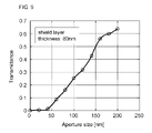
- FIG. 9 illustrates the relation between total transmittance and aperture size. Although a larger aperture shows high transmittance, the resolution will be poor when applied for aerial image measurement. Thus, there is a trade-off relationship between the aperture transmittance and the resolution. Therefore, one method is to determine the aperture size considering a target image size for the measurement. In the example illustrated in FIG. 9 calculations assumed a shield layer thickness of 80 nm
- FIG. 10 illustrates the relation between total transmittance and shield layer thickness.
- the transmittance from an aperture becomes larger when a shield layer (also referred to as a light-shielding layer) becomes thinner.
- a shield layer also referred to as a light-shielding layer
- the performance as a shield layer is degraded.
- a portion of light impinging on a shield layer penetrates the layer, creating noises in measurement signals.
- One method is to determine the thickness of a shield layer by considering its light shielding performance.
- FIG. 11 illustrates the relation between total transmittance and shield layer thickness as a function of index of refraction of the material in an aperture.
- One way to improve transmittance is to fill the aperture space with a material that has high refractive index.
- Note that further improvement of transmittance can be expected by filling the aperture space with AlN (aluminum nitride) whose refractive index is 2.423 at the wavelength of 193 nm.
- the amount of light that reaches the detector can be controlled by the number of apertures in an array.
- the light intensity is proportional to the aperture number, and the aperture number is determined so that the total light intensity surpasses the minimum intensity that is required by the sensitivity of a detector.
- multiple arrays that are allocated with the same or the integral multiple period as that of the image can be used to enhance the amount of light reaching the detector.
- a first example of the second exemplary embodiment is directed to a detection aperture which includes a 2-D aperture array that can have variable thickness effective refractive index aperture material
- a second example of the second exemplary embodiment is directed to varying the pitch between at least a few of the apertures in the 2-D aperture array
- a third example includes a 2-D aperture array which includes at least two 1-D aperture arrays each slightly non aligned with respect to the other along the 1-D direction, improving the detected resolution and/or intensity of the sampled image
- a third example includes a 2-D aperture array where the aperture material can be varied in refractive index and thickness to improve the matching TE and TM. Note that in the first and second exemplary embodiments the aperture sizes and shapes can vary.
- FIG. 12A illustrates an example of a detection aperture 900 in accordance with at least one exemplary embodiment.
- An image 905 carried by image light is incident on a cover layer 910 (optional, e.g., SiO2), which covers a shield layer 920 .
- the shield layer 920 contains a plurality of apertures 950 , which can be filled with material, either fully or partially in accordance with at least one exemplary embodiment.
- the shield layer can rest on a support layer 930 through which the light passing through the apertures 950 can pass.
- the light can be collimated by a lens 970 , and to a sensor 960 of a detector.
- the entire detector aperture 900 can be moved 990 in a scanning direction.
- a detector aperture in accordance with the second exemplary embodiment is similar to the first exemplary embodiment, which can include a shield layer and an aperture array, where the aperture array is placed in the shield layer, where the second exemplary embodiment includes a 2-D aperture array which can include at least one of varying thickness aperture material, a pitch between apertures, and offset 1-D arrays comprising the 2-D array.
- Further detector apertures in accordance with the second exemplary embodiment can include a cover layer, and a support layer.
- the cover layer can have one side exposed to a fluid medium (e.g., air, water) or vacuum.
- FIGS. 12B and 12C illustrate top views of two examples of a 2-D aperture array in accordance with the second exemplary embodiment.
- An alignment line AL passes through the center of an aperture in a second linear aperture array LA 2 .
- AL passes through the center of a neighboring aperture in first linear array LA 1 , aligning the two linear aperture arrays LA 1 and LA 2 .
- AL does not pass through the center of a neighboring aperture in the LA 1 , thus in this example LA 1 and LA 2 are offset or non-aligned.
- an error in fabrication misaligns neighboring linear arrays, over an extent the errors can even out if the error is both positive and negative with respect to the desired alignment.
- the shape of apertures are various due to manufacturing errors the offset arrangement illustrated in FIG. 12C can average out the effects of the various shapes.
- FIG. 13 A illustrates a comparison between a first set of apertures 1350 a of a first linear aperture array and a second set of apertures 1350 b of a second linear aperture array.
- the first set of apertures has a circular shape while the second set of apertures has a square shape.
- FIG. 13B illustrates the transmittance comparison between the two different shapes of apertures.
- the square aperture has a higher transmittance level as a function of aperture size, where the aperture size is measured as a side of the square or the diameter of the circle.
- apertures can take the form of more complicated shapes.
- FIG. 13C illustrates an example of various complicated aperture shapes associated with particular linear aperture arrays (LA 1 a - e ). Other than a simple square shape, more peculiar shapes may be applied. For example, it is known that a “C-shaped” aperture shows higher transmittance than a circular or a square aperture under certain circumstances. For detailed properties of a C-shaped aperture, “Ultrahigh light transmission through a C-shaped nanoaperture”, Optics Letters, Vol. 28, No. 15 (2003) by Xiaolei Shi, etc. can be referred to.
- Linear arrays LA 1 a - e illustrate various orientations of C-Shaped apertures in accordance with at least one exemplary embodiment.
- FIG. 14 illustrates a method of fabrication of an aperture array in accordance with at least one exemplary embodiment.
- a photoresist is deposited on a substrate (S 1 ) that is composed of a supporting substrate and shield layer.
- a photoresist e.g., positive or negative photoresist
- the reticle has a pattern corresponding to the desired aperture array.
- the exposed photoresist is then developed (S 2 ) and etched (S 3 ) to form etched recesses in the shield layer of the substrate corresponding to apertures in an aperture array.
- the recesses are filled or partially filled (S 4 ) with a material to vary the recess's index of refraction to a designed value.
- the excess material on the surface of the substrate is removed (e.g., finished S 5 ) and the filled material removed if extending beyond the recess so that the surface is generally planar.
- At least one exemplary embodiment can have at least one aperture filled with at least one of AlN, SiO2, Cr2O3, HfO2, and Si3N4.
- a detector aperture array in accordance with exemplary embodiments can use various materials, for example Cr, Si, Mo, Ta, W, Rh, MoN, NbN, other materials as known by one of ordinary skill in the relevant art and equivalents.
Abstract
At least one exemplary embodiment is directed to detection aperture array which includes a shield layer; and a plurality of apertures, where the plurality of apertures are formed in the shield layer and filled with a first medium having an effective index of refraction, wherein the plurality of apertures includes at least two apertures separated by a pitch, wherein the plurality of apertures has a measurement value wherein the measurement value includes at least one of the effective refractive index and a pitch value, wherein the measurement value is changed so that TM and TE modes in incident image light passes through the plurality of apertures with about the same transmittance level, wherein when the measurement value is the pitch value then the TM and TE transmittance level are about the same when an angle of incidence of an image light varies.
Description
The present invention relates to a method/apparatus configured to measure and/or improve detected resolution and/or intensity of a sampled image. More particularly, though not exclusively, the present invention is related to aperture arrays and/or varying aperture properties to improve detection resolution and/or detection intensity of an image of a reticle pattern.
The resolution R of the conventional system illustrated in FIG. 1 is determined by its projection lens 150 numerical aperture (NA) and the illumination (exposure) wavelength (λ). The relationship can be expressed as:
R=(k1λ)/NA (1)
R=(k1λ)/NA (1)
where k1 is a process dependent factor (e.g., between 0.3-0.5). For example, a NA of over 1.0 can be obtained using an immersion system. ArF laser (A=193 nm) is typically used as the illumination system. For an immersion system the space 165 between the projection lens 150 and the wafer 170 is filled with fluid. The fluid can be transparent to the illumination wavelength and have an index of refraction “n” greater than 1 (e.g., purified water n=1.44). Note that when the term fluid is referred to herein it can include liquids (e.g., water) and gases (e.g., air at various pressures).
One method of conventional detection to acquire the image accuracy is to expose the photoresist, develop the photoresist, and view it under a scanning electron microscope (SEM). However several photoresist properties in addition to the desire to sample the image directly have led to the development of sampling detection arrangements.
When using a single aperture, a non-periodic image (as opposed to the periodic image illustrated in FIG. 2A ) can be detected. For example FIG. 2B illustrates a single slit system as illustrated in FIG. 2A , as applied to a non-periodic multiple intensity image 210 b.
In the case of a periodic image in the scan direction a multi slit system can be used. FIG. 2C illustrates a conventional multi slit 220 b (multi-aperture) image sampling detection arrangement 200 b (detector aperture). This arrangement is similar to the single aperture arrangement but with multiple slits to sample a periodic image. Both arrangements can be moved to sample the entire image. Since the image is periodic, each aperture practically captures the same image portion. The arrangement in FIG. 2C allows more light, compared with the single slit arrangement in FIG. 2A , to be detected by the detector. Again the image 210 c is sampled by a detector 260 b that detects the portion of the image light 250 b passing through the detector aperture 200 b, i.e. the portion passing through the multi-apertures 220 b. The other portions not being transmitted through the detector aperture 200 b are shielded by the shield layer 230 b, which is supported by the support substrate 240 b.
In several conventional arrangements the aperture width (e.g., a slit width) is smaller than the image light wavelength so that image features can be detected. U.S. Pat. No. 5,631,731 discusses a single slit aperture arrangement and a multi-slit arrangement. Note that the term aperture is used to denote an opening, a slit, a hole, and any other type of region that allows a particular frequency of light to pass while other neighboring regions do not. Since the aperture width tends to be smaller than the wavelength of the image light, diffraction can occur upon exiting the aperture(s), adding to image detection errors at the detector (e.g., reduced accuracy, reduced intensity). Reduced accuracy of measurement can occur when different polarizations of the image light, each having different levels of contrast, are transmitted differently through the detector aperture. Reduced intensity can occur when only a portion of the diffracted light reaches the detector. Reduced intensity can also be a function of angle of incidence.
As discussed above the different polarizations TM and TE can have different transmittance properties through an aperture. FIG. 3B illustrates the relative transmittance of TE and TM polarized image light through the narrow aperture 320 of the detector aperture 300 of FIG. 3A . The plots are based upon a simulation (solving Maxwell's Equations using Finite Difference Time Domain (FDTD) method) where the conditions assumed are:
that the shielding material is Cr, where the optical properties are n=0.841, and k=1.647;
where the illumination light has a wavelength of λ=193 nm (e.g., ArF laser);
where the thickness of the shielding later is about 95 nm; and
where the aperture is a slit and is varied from 15 nm to 235 nm.
As is illustrated in FIG. 3B the transmittance for the TE and TM modes are different for various slit widths, and match at a slit width of about 60 nm. However to determine features in the image light it is often useful to have a slit width smaller than 60 nmn, for example 45 nm. At 45 nm though the TM transmittance is higher than the TE transmittance. Notice that at 45 nm the transmittance level of both modes have decreased.
To illustrate reduced intensity due to diffractive effects on the transmitted image light, a detector is moved to two positions A1 and A2 (FIG. 3A ) and the image light measured and plotted in FIGS. 3C and 3D respectively.
Additionally variation in transmitted intensity, through a 1-D slit, between TE and TM can occur as the incident angle θ varies. FIG. 3E illustrates the angular and polarization dependence of transmittance as determined via simulation where (referring to FIG. 3A ) the aperture 320 is a cross-section of a 1 D slit filled with SiO2; the aperture width d>=50 nm; the shield layer 310 is made of Tantalum with a thickness W1>=80 nm; the medium 310A is water; and the medium 310B is SiO2. As can be seen the TE and TM polarizations have different transmission properties. With the transmittance of both modes approach each other in value as the incidence angle increases. For accurate measurements, the transmittance between the TE and TM polarizations needs to be matched including their angular behaviors. One solution to this issue has been discussed in application 10025281US01(100-3365) filed on Oct. 21, 2005, which discusses matching the transmittance of the TE and TM polarizations by properly adjusting the effective refractive index in an aperture space. By controlling the volume ratio between mediums (e.g., air and/or other materials) in the aperture (for example, the same material as substrate), the refractive index in the aperture space can be effectively controlled. In the discussed system to avoid intrusion of a liquid medium into the aperture space (e.g., if part of the medium in the aperture is air) a cover plate can be used. Additionally, with the discussed system, the fabrication method can be difficult to obtain a partially filled aperture.
In addition to diffraction's reduction of the detected image intensity, the various transmittances of the TE and TM mode can result in reduced accuracy in the measurement. For example FIG. 4A illustrates the image 420 a from TE polarized image light 410 a.
At least one exemplary embodiment is directed to a detection aperture array that substantially matches the TE and TM polarizations by replacing a 1-D slit with a 1-D aperture array, improving the detected resolution and/or intensity of the sampled image.
At least one exemplary embodiment is directed to a detection aperture array that substantially matches the transmission properties between the TE and TM polarizations by using a 1-D aperture array which includes apertures of varying shape and size, improving the detected resolution and/or intensity of the sampled image.
At least one exemplary embodiment is directed to a detection aperture array that substantially matches the transmission properties between the TE and TM polarizations by using a 2-D aperture array, improving the detected resolution and/or intensity of the sampled image.
At least one exemplary embodiment is directed to a detection aperture array that substantially matches the transmission properties between the TE and TM polarizations by using a 2-D aperture array, wherein the 2-D aperture array includes at least two 1-D aperture arrays each slightly non aligned with respect to the other along the 1-D direction, improving the detected resolution and/or intensity of the sampled image.
At least one exemplary embodiment is directed to a detection aperture array that substantially matches the transmission properties between the TE and TM polarizations by varying the aperture index of refraction improving the detected resolution and/or intensity of the sampled image.
At least one exemplary embodiment is directed to methods of fabrication of aperture arrays of exemplary embodiments.
Further areas of applicability of exemplary embodiments of the present invention will become apparent from the detailed description provided hereinafter. It should be understood that the detailed description and specific examples, while indicating exemplary embodiments of the invention, are intended for purposes of illustration only and are not intended to limit the scope of the invention.
Exemplary embodiments of present invention will become more fully understood from the detailed description and the accompanying drawings.
The following description of at least one exemplary embodiment is merely illustrative in nature and is in no way intended to limit the invention, its application, or uses.
Exemplary embodiments can be used with any image sampling or detection system and are not limited to those discussed in the illustrative examples herein.
Processes, techniques, apparatus, and materials as known by one of ordinary skill in the art may not be discussed in detail but are intended to be part of the enabling description where appropriate. For example semiconductor etching materials and procedures may not be discussed in detail (e.g., using positive or negative photoresists), however one of ordinary skill would be able, without undo experimentation, to use such materials and procedures, given the enabling disclosure herein, to construct detection aperture devices in accordance with exemplary embodiments. Such procedures and materials are intended to fall within the scope of exemplary embodiments.
Also note that exemplary embodiments can also be applied to any imaging apparatus that samples an image through an aperture, (e.g., a microscope) and thus, are not limited to the example uses described herein.
Notice that similar reference numerals and letters refer to similar items in the following figures, and thus once an item is defined in one figure, it may not be discussed or further defined in the following figures.
Two exemplary embodiments are discussed herein with associated examples and a method of fabrication. However these exemplary embodiments are not meant to be limitative of the number of exemplary embodiments but instead are included for illustrative purposes.
The first exemplary embodiment is directed to a 1-D detection aperture array, where in a first example of a first exemplary embodiment the pitch between the apertures in the aperture array are varied to improve the relative transmittance of TE and TM modes (i.e., substantially match) passing through the aperture array.
In a second example of a first exemplary embodiment, the thickness of the refractive material in the apertures of the aperture array is varied to improve the relative transmittance of TE and TM modes passing through the aperture array.
Additional examples of the first exemplary embodiment matches the transmission properties between the TE and TM polarizations by using a 1-D aperture array which includes apertures of varying shape and size, improving the detected resolution and/or intensity of the sampled image.
A first example of the second exemplary embodiment is directed to a detection aperture array that substantially matches the transmission properties between the TE and TM polarizations by using a 2-D aperture array where the apertures refractive material's thickness can be varied, improving the detected resolution and/or intensity of the sampled image.
A second example of the second exemplary embodiment is directed to a detection aperture array that substantially matches the transmission properties between the TE and TM polarizations by varying the pitch between apertures in a 2-D aperture array.
Additional examples of the second exemplary embodiment is directed to a detection aperture array that matches the transmission properties between the TE and TM polarizations by using a 2-D aperture array, wherein the 2-D aperture array includes at least two 1-D aperture arrays each slightly non aligned with respect to the other along the 1-D direction, improving the detected resolution and/or intensity of the sampled image.
The first exemplary embodiment is directed to a detection 1-D aperture array that can include apertures of varying shape and size, apertures with varying thickness of aperture material, and varying pitch between apertures, improving the detected resolution and/or intensity of the sampled image.
The first example of the first exemplary embodiment substantially matches the transmittance between the TE and TM polarizations, by properly adjusting the aperture refractive index, in each aperture of an aperture array, between 1 (e.g., air or vacuum) and that of a substrate (e.g., SiO2, n=1.56). FIGS. 6A , 6B, 7A, 7B, 8A-8C, 13A, and 13C illustrate several non-limiting examples in accordance with the first exemplary embodiment. To adjust the aperture effective refractive index, a material can be added in each aperture of a plurality of apertures, for example SiO2, MgF2, LiF, and other materials to adjust the index of refraction as known by one of ordinary skill in the relevant art and equivalents.
An example of a slit detection aperture 500, is illustrated in FIG. 5A . Aspects of the slit detection aperture (e.g., shield layer material, second aperture material) can also be used in exemplary embodiments and features of FIGS. 5A and 5B are used as illustrative examples of general arrangements and materials, where the first and second exemplary embodiments are directed to aperture arrays, where the apertures can be of various shapes. In FIG. 5A , a shield layer 540 has an aperture with a first aperture material 530 and a second aperture material 560 inserted. The aperture is one of a plurality of non-slit apertures extending into and out of the paper. The second aperture material has a thickness of “t1” and a width of “d.” The shield layer 540 can be covered by a cover layer 520 (e.g., SiO2) that is substantially transparent to the wavelength of the image light and can hold in the aperture materials or prevent other materials from entering the aperture. Note that in general the aperture can be filled completely with the second aperture material, and thus a cover layer 520 may not be included. The cover layer 520 is exposed on the opposite side to the aperture to an adjacent medium 510 that can vary depending upon the device or its usage (e.g., purified water, air, vacuum), and the shield layer 540 can be supported by a support layer 550 that is operatively connected to the shield layer 540 on the side opposite the cover layer 520. Setting the aperture size (e.g., each individual aperture's size) to a desired value and varying the thickness t1 can result in varying the transmittance of TE and TM modes through the aperture array.
Although the first and second exemplary embodiments are generally directed to an array of apertures, for illustrative purposes FIG. 5B illustrates the relative transmittance of TE and TM polarized image light through a detection aperture where the aperture is a single slit with the simulation conditions of:
for an adjacent medium 510 of water (n=1.44, k=0);
where the light shield layer 540 is made of Cr, with a thickness (W) of 80 nm, where 80 nm has been chosen so that the transmittance of light through the shield layer is less than 0.001;
where support layer 550 is SiO2 (n=1.56, k=0);
where the cover layer 520 is also SiO2, and prohibits water from the adjacent medium 510 from entering the aperture;
the aperture is a slit with a width (d) of 45 nm, where the theoretical image resolution is 22.5 nm; and
where the thickness (t1) is varied from 0 to 80 nm, where the material for the second aperture medium 560 is SiO2 and the material of the first aperture medium 530 is air. Note that these values are for illustrative purposes only and other various dimensional values and materials can be used within the scope of the exemplary embodiments.
Thus likewise in the case of the first example of the first exemplary embodiment, the apertures (e.g., recesses in the shield layer 540) can be completely filled with a material having a thickness t1 equal to the shield layer 540 width W. Additionally instead of a slit as in the illustrative example of FIG. 5A , the first example of the first exemplary embodiment and the first example of the second exemplary embodiment are directed to a plurality of individual apertures that can be arranged in a 1-D or 2-D array in the shield layer 540 with varying refractive thicknesses as illustrated in FIGS. 5A-5B , for example FIG. 3E and FIGS. 6C-6D are simulated using circular apertures (see FIGS. 6A-6B ) in an aperture array.
The second example of an aperture array in accordance with the first exemplary embodiment substantially matches the transmittance between the TE and TM polarizations by properly controlling the pitch of the 1-D aperture array, likewise in the second example of the second exemplary embodiment (2-D aperture array) the pitch between apertures can be controlled. FIG. 6A illustrates a second example of an aperture array (also referred to as a detection aperture array) in accordance with the first exemplary embodiment. As illustrated instead of using a 1-dimensional slit, the first exemplary embodiment is directed to a 1-D array 620 of a plurality of apertures (A1-A5) formed in a shield layer 610. A bird's eye view of the same structure is presented in FIG. 6B . The aperture array 620 is represented by the size of each aperture in the aperture array and the pitch between adjacent apertures. The array 620 is assumed to lie along the y direction, although the array can be non-linear as well (e.g., S-shaped). The terminologies TE/TM polarizations are used in the same manner as the case of a simple aperture slit as discussed with respect to FIG. 5B . In the particular example illustrated the TE mode is arranged substantially parallel with the y-axis, while the TM mode is arranged substantially parallel with the x-axis, although exemplary embodiments are not so limited.
The amount of light that reaches the detector can be controlled by the number of apertures in an array. The light intensity is proportional to the aperture number, and the aperture number is determined so that the total light intensity surpasses the minimum intensity that is required by the sensitivity of a detector.
When an image is periodic, multiple arrays that are allocated with the same or the integral multiple period as that of the image can be used to enhance the amount of light reaching the detector.
A first example of the second exemplary embodiment is directed to a detection aperture which includes a 2-D aperture array that can have variable thickness effective refractive index aperture material, while a second example of the second exemplary embodiment is directed to varying the pitch between at least a few of the apertures in the 2-D aperture array, while a third example includes a 2-D aperture array which includes at least two 1-D aperture arrays each slightly non aligned with respect to the other along the 1-D direction, improving the detected resolution and/or intensity of the sampled image and a third example includes a 2-D aperture array where the aperture material can be varied in refractive index and thickness to improve the matching TE and TM. Note that in the first and second exemplary embodiments the aperture sizes and shapes can vary.
As discussed above with respect to the first exemplary embodiment, further exemplary embodiments are not limited to a detection aperture array having only one dimension. Multiple dimensional aperture arrays are intended to lie within the scope of the exemplary embodiments. FIG. 12A illustrates an example of a detection aperture 900 in accordance with at least one exemplary embodiment. An image 905 carried by image light is incident on a cover layer 910 (optional, e.g., SiO2), which covers a shield layer 920. The shield layer 920 contains a plurality of apertures 950, which can be filled with material, either fully or partially in accordance with at least one exemplary embodiment. The shield layer can rest on a support layer 930 through which the light passing through the apertures 950 can pass. The light can be collimated by a lens 970, and to a sensor 960 of a detector. The entire detector aperture 900 can be moved 990 in a scanning direction.
In summary, a detector aperture in accordance with the second exemplary embodiment is similar to the first exemplary embodiment, which can include a shield layer and an aperture array, where the aperture array is placed in the shield layer, where the second exemplary embodiment includes a 2-D aperture array which can include at least one of varying thickness aperture material, a pitch between apertures, and offset 1-D arrays comprising the 2-D array.
Further detector apertures in accordance with the second exemplary embodiment can include a cover layer, and a support layer. In at least one exemplary embodiment the cover layer can have one side exposed to a fluid medium (e.g., air, water) or vacuum.
As mentioned previously, apertures in exemplary embodiments can be deliberately fabricated in different shapes. For example FIG. 13 A illustrates a comparison between a first set of apertures 1350 a of a first linear aperture array and a second set of apertures 1350 b of a second linear aperture array. The first set of apertures has a circular shape while the second set of apertures has a square shape.
At least one exemplary embodiment can have at least one aperture filled with at least one of AlN, SiO2, Cr2O3, HfO2, and Si3N4.
A detector aperture array in accordance with exemplary embodiments can use various materials, for example Cr, Si, Mo, Ta, W, Rh, MoN, NbN, other materials as known by one of ordinary skill in the relevant art and equivalents.
While the present invention has been described with reference to exemplary embodiments, it is to be understood that the invention is not limited to the disclosed exemplary embodiments. The scope of the following claims is to be accorded the broadest interpretation so as to encompass all modifications, equivalent structures and functions. For example, if words such as “orthogonal”, “perpendicular” are used the intended meaning is “substantially orthogonal” and “substantially perpendicular” respectively. Additionally although specific numbers may be quoted in the claims, it is intended that a number close to the one stated is also within the intended scope, i.e. any stated number (e.g., 90 degrees) should be interpreted to be “about” the value of the stated number (e.g., about 90 degrees).
Claims (14)
1. A detection aperture array comprising:
a shield layer; and
a plurality of apertures, wherein the plurality of apertures are formed in the shield layer and filled with a first medium having an effective index of refraction, wherein the plurality of apertures includes at least two apertures separated by a pitch, wherein the plurality of apertures has a measurement value wherein the measurement value includes at least one of the effective refractive index and a pitch value, wherein the measurement value is changed so that TM and TE modes in incident image light passes through the plurality of apertures with about the same transmittance level, wherein when the measurement value is the pitch value then the TM and TE transmittance level are about the same when an angle of incidence of an image light varies, wherein the effective index of refraction is higher than 1.
2. The detection aperture array according to claim 1 , wherein the plurality of apertures are arranged in a linear 1-D array.
3. The detection aperture array according to claim 1 , wherein the plurality of apertures are arranged in a 2-D array of at least two linear 1-D arrays.
4. The detection aperture array according to claim 3 , wherein the at least two linear 1-D arrays are substantially parallel to each other.
5. The detection aperture array according to claim 1 , wherein the at least two apertures have different comparative sizes.
6. The detection aperture array according to claim 1 , wherein the first medium is at least one of SiO2, LiF, MgF2, AlN, Cr2O3, HfO2, and Si3N4.
7. The detection aperture array according to claim 1 , wherein the shield layer is made from a shield medium, wherein the shield medium is at least one of Cr, Si, Mo, Ta, W, Rh, MoN, and NbN.
8. The detection aperture according to claim 7 , wherein the thickness of the shield layer is between 25 and 160 nm.
9. The detection aperture according to claim 8 , wherein the shield medium is chosen based upon which material provides a lower transmission of TE and TM polarized light through the shield layer for a given thickness.
10. The detection aperture array according to claim 1 , further comprising:
a support substrate, wherein the support substrate is operatively connected to one side of the shield layer, and wherein the index of refraction of the support substrate is less than the effective index of refraction.
11. A detection aperture array comprising:
a shield layer; and
a plurality of apertures, wherein the plurality of apertures are formed in the shield layer and filled with a first medium having an effective index of refraction, wherein the plurality of apertures includes at least two apertures separated by a pitch, wherein the plurality of apertures has a measurement value wherein the measurement value includes at least one of the effective refractive index and a pitch value, wherein the measurement value is changed so that TM and TE modes in incident image light passes through the plurality of apertures with about the same transmittance level, wherein when the measurement value is the pitch value then the TM and TE transmittance level are about the same when an angle of incidence of an image light varies, wherein the at least two apertures have different comparative shapes or different comparative sizes.
12. A detection aperture array comprising:
a shield layer; and
a plurality of apertures, wherein the plurality of apertures are formed in the shield layer and filled with a first medium having an effective index of refraction, wherein the plurality of apertures includes at least two apertures separated by a pitch, wherein the plurality of apertures has a measurement value wherein the measurement value includes at least one of the effective refractive index and a pitch value, wherein the measurement value is changed so that TM and TE modes in incident image light passes through the plurality of apertures with about the same transmittance level, wherein when the measurement value is the pitch value then the TM and TE transmittance level are about the same when an angle of incidence of an image light varies, wherein the plurality of apertures are arranged in a 2-D array of at least two linear 1-D arrays, wherein the at least two linear 1-D arrays are substantially parallel to each other, wherein a first linear 1-D array and a second linear 1-D array of the 2-D array, include a respective first set of apertures and a second set of apertures, wherein the first set of apertures are offset with respect to the second set of apertures.
13. The detection aperture away according to claim 12 , wherein the first set of apertures includes individual apertures separated by a pitch greater than 100 nm.
14. The detection aperture away according to claim 13 , wherein the individual apertures of the first set of apertures have a size between 24 nm and about 200 nm.
Priority Applications (1)
| Application Number | Priority Date | Filing Date | Title |
|---|---|---|---|
| US11/531,431 US7508598B2 (en) | 2006-09-13 | 2006-09-13 | Apparatus for measuring aerial images produced by an optical lithography system |
Applications Claiming Priority (1)
| Application Number | Priority Date | Filing Date | Title |
|---|---|---|---|
| US11/531,431 US7508598B2 (en) | 2006-09-13 | 2006-09-13 | Apparatus for measuring aerial images produced by an optical lithography system |
Publications (2)
| Publication Number | Publication Date |
|---|---|
| US20080074758A1 US20080074758A1 (en) | 2008-03-27 |
| US7508598B2 true US7508598B2 (en) | 2009-03-24 |
Family
ID=39224649
Family Applications (1)
| Application Number | Title | Priority Date | Filing Date |
|---|---|---|---|
| US11/531,431 Expired - Fee Related US7508598B2 (en) | 2006-09-13 | 2006-09-13 | Apparatus for measuring aerial images produced by an optical lithography system |
Country Status (1)
| Country | Link |
|---|---|
| US (1) | US7508598B2 (en) |
Cited By (3)
| Publication number | Priority date | Publication date | Assignee | Title |
|---|---|---|---|---|
| CN101957561A (en) * | 2009-06-19 | 2011-01-26 | Asml荷兰有限公司 | Sensor, table and lithographic apparatus |
| US20110222041A1 (en) * | 2010-03-12 | 2011-09-15 | Canon Kabushiki Kaisha | Apparatus, method, and lithography system |
| US20120257183A1 (en) * | 2005-09-15 | 2012-10-11 | Franklin Mark Schellenberg | Nanolithography system |
Families Citing this family (1)
| Publication number | Priority date | Publication date | Assignee | Title |
|---|---|---|---|---|
| US8432530B2 (en) * | 2008-07-22 | 2013-04-30 | Canon Kabushiki Kaisha | Device, method, and system for measuring image profiles produced by an optical lithography system |
Citations (1)
| Publication number | Priority date | Publication date | Assignee | Title |
|---|---|---|---|---|
| US5631731A (en) | 1994-03-09 | 1997-05-20 | Nikon Precision, Inc. | Method and apparatus for aerial image analyzer |
-
2006
- 2006-09-13 US US11/531,431 patent/US7508598B2/en not_active Expired - Fee Related
Patent Citations (2)
| Publication number | Priority date | Publication date | Assignee | Title |
|---|---|---|---|---|
| US5631731A (en) | 1994-03-09 | 1997-05-20 | Nikon Precision, Inc. | Method and apparatus for aerial image analyzer |
| US5866935A (en) | 1994-03-09 | 1999-02-02 | Nikon Precision, Inc. | Tunneling device |
Cited By (7)
| Publication number | Priority date | Publication date | Assignee | Title |
|---|---|---|---|---|
| US20120257183A1 (en) * | 2005-09-15 | 2012-10-11 | Franklin Mark Schellenberg | Nanolithography system |
| US8507881B2 (en) * | 2005-09-15 | 2013-08-13 | Franklin Mark Schellenberg | Nanolithography system |
| US9229330B2 (en) | 2005-09-15 | 2016-01-05 | Franklin Mark Schellenberg | Method for writing nanoscale patterns |
| US10539880B2 (en) | 2005-09-15 | 2020-01-21 | Franklin Mark Schellenberg | Method and system for nanoscale data recording |
| CN101957561A (en) * | 2009-06-19 | 2011-01-26 | Asml荷兰有限公司 | Sensor, table and lithographic apparatus |
| TWI417678B (en) * | 2009-06-19 | 2013-12-01 | Asml Netherlands Bv | A sensor, a table and lithographic apparatus |
| US20110222041A1 (en) * | 2010-03-12 | 2011-09-15 | Canon Kabushiki Kaisha | Apparatus, method, and lithography system |
Also Published As
| Publication number | Publication date |
|---|---|
| US20080074758A1 (en) | 2008-03-27 |
Similar Documents
| Publication | Publication Date | Title |
|---|---|---|
| US7230703B2 (en) | Apparatus and method for measuring overlay by diffraction gratings | |
| JP4222926B2 (en) | Device inspection | |
| KR101368523B1 (en) | System for measuring the image quality of an optical imaging system | |
| US6674511B2 (en) | Evaluation mask, focus measuring method and aberration measuring method | |
| US5859424A (en) | Apodizing filter system useful for reducing spot size in optical measurements and other applications | |
| TWI525315B (en) | Phase-controlled model-based overlay measurement systems and methods | |
| TWI461857B (en) | Method and apparatus for angular-resolved spectroscopic lithography characterization | |
| US20040229471A1 (en) | Periodic patterns and technique to control misalignment between two layers | |
| JP6429817B2 (en) | Projection exposure tool for microlithography and method of microlithography imaging | |
| TW201708972A (en) | Inspection apparatus, inspection method, lithographic apparatus, patterning device and manufacturing method | |
| US7443515B2 (en) | Apparatus for measuring optical properties of tested optical system using interference | |
| CN109196420B (en) | Pattern forming apparatus | |
| TW201708934A (en) | Method of metrology, inspection apparatus, lithographic system and device manufacturing method | |
| US20100215273A1 (en) | Methods and devices for characterizing polarization of illumination system | |
| US7692799B2 (en) | Measurement apparatus, exposure apparatus, and device fabrication method | |
| US5789118A (en) | Method and apparatus for precision determination of phase-shift in a phase-shifted reticle | |
| US7508598B2 (en) | Apparatus for measuring aerial images produced by an optical lithography system | |
| US5700602A (en) | Method and apparatus for precision determination of phase-shift in a phase-shifted reticle | |
| US7911709B2 (en) | Apparatus and method for improving detected resolution and/or intensity of a sampled image | |
| US20070019175A1 (en) | Exposure apparatus and device manufacturing method using the apparatus | |
| US8085393B2 (en) | Exposure apparatus inspection method and method for manufacturing semiconductor device | |
| US7474413B2 (en) | Method and apparatus for analyzing interference fringe | |
| JP4109832B2 (en) | Exposure mask and focus monitor method | |
| KR20210016439A (en) | Sensor device and method for lithographic measurements | |
| US7642016B2 (en) | Phase calibration for attenuating phase-shift masks |
Legal Events
| Date | Code | Title | Description |
|---|---|---|---|
| AS | Assignment |
Owner name: CANON KABUSHIKI KAISHA, JAPAN Free format text: ASSIGNMENT OF ASSIGNORS INTEREST;ASSIGNOR:UNNO, YASUYUKI;REEL/FRAME:018246/0745 Effective date: 20060912 |
|
| FEPP | Fee payment procedure |
Free format text: PAYOR NUMBER ASSIGNED (ORIGINAL EVENT CODE: ASPN); ENTITY STATUS OF PATENT OWNER: LARGE ENTITY |
|
| FPAY | Fee payment |
Year of fee payment: 4 |
|
| REMI | Maintenance fee reminder mailed | ||
| LAPS | Lapse for failure to pay maintenance fees | ||
| STCH | Information on status: patent discontinuation |
Free format text: PATENT EXPIRED DUE TO NONPAYMENT OF MAINTENANCE FEES UNDER 37 CFR 1.362 |
|
| FP | Lapsed due to failure to pay maintenance fee |
Effective date: 20170324 |