US7498860B2 - Buffer circuit having multiplexed voltage level translation - Google Patents
Buffer circuit having multiplexed voltage level translation Download PDFInfo
- Publication number
- US7498860B2 US7498860B2 US11/691,590 US69159007A US7498860B2 US 7498860 B2 US7498860 B2 US 7498860B2 US 69159007 A US69159007 A US 69159007A US 7498860 B2 US7498860 B2 US 7498860B2
- Authority
- US
- United States
- Prior art keywords
- circuit
- signal
- voltage level
- mode
- output
- Prior art date
- Legal status (The legal status is an assumption and is not a legal conclusion. Google has not performed a legal analysis and makes no representation as to the accuracy of the status listed.)
- Active
Links
Images


Classifications
-
- H—ELECTRICITY
- H03—ELECTRONIC CIRCUITRY
- H03K—PULSE TECHNIQUE
- H03K19/00—Logic circuits, i.e. having at least two inputs acting on one output; Inverting circuits
- H03K19/0175—Coupling arrangements; Interface arrangements
- H03K19/017581—Coupling arrangements; Interface arrangements programmable
-
- H—ELECTRICITY
- H03—ELECTRONIC CIRCUITRY
- H03K—PULSE TECHNIQUE
- H03K19/00—Logic circuits, i.e. having at least two inputs acting on one output; Inverting circuits
- H03K19/0175—Coupling arrangements; Interface arrangements
- H03K19/01759—Coupling arrangements; Interface arrangements with a bidirectional operation
Definitions
- the present invention relates generally to electronic circuits, and more particularly relates to bidirectional buffer circuits.
- circuitry utilized with such portable devices may be configured so that a portion of the circuitry, such as, for example, input/output (IO) buffers, runs at a higher voltage level (e.g., about 3.3 volts), as may be supplied by an IO voltage source, while another portion of the circuitry, such as, for example, core logic, runs at a substantially lower voltage level (e.g., about 1.0 volt), as may be supplied by a core voltage source.
- IO input/output
- core logic runs at a substantially lower voltage level (e.g., about 1.0 volt)
- This difference in voltage levels often necessitates the use of a voltage level translator circuit for interfacing between the multiple voltage levels.
- bidirectional buffer circuits include an input stage and an output stage.
- Some bidirectional buffer circuits utilize programmable control signals (e.g, buffer enable, pull-up, pull-down, etc.) generated, for example, by core logic circuitry that are applied to both the input and output stages of the buffer.
- Each of these control signals requires voltage level translation, typically by way of a voltage level translator circuit, in order to change the voltage level of the signal from the lower core voltage level to the higher voltage level of the IO driver.
- each voltage level translator circuit consumes a significant amount of chip area in an integrated circuit device, and therefore the number of voltage level translator circuits in the integrated circuit should be minimized.
- the present invention meets the above-noted need by providing, in an illustrative embodiment thereof, an enhanced buffer circuit having reduced chip area compared to standard buffer circuits.
- an embodiment of the invention utilizes multiplexing of two or more control signals supplied to the buffer circuit so as to share a single voltage level translator circuit, thereby utilizing a fewer number of voltage level translator circuits and reducing the overall size of the integrated circuit.
- a buffer circuit is selectively operative in one of at least a first mode and a second mode as a function of a first control signal supplied to the buffer circuit.
- the buffer circuit includes interface circuitry operative to receive at least second and third control signals referenced to a first voltage level, and to generate an output signal referenced to a second voltage level, the second voltage level being greater than the first voltage level.
- the output signal is a function of the second control signal in the first mode and is a function of the third control signal in the second mode.
- the buffer circuit further includes at least first and second circuit portions coupled to the interface circuitry, each of the first and second circuit portions including at least one control input operative to receive the output signal generated by the interface circuitry. At least a portion of the buffer circuit may be implemented in an integrated circuit.
- the interface circuitry preferably includes at least one voltage level translator circuit operative to receive, as a function of the first control signal, one of at least the second and third control signals, and to generate the output signal.
- At least one operating characteristic of the first circuit portion may be controllable in the first mode as a function of the second control signal and a least one operating characteristic of the second circuit portion may be controllable in the second mode as a function of the third control signal.
- an operation of the first circuit portion is substantially unaffected by application of the output signal of the voltage level translator circuit to the second circuit portion in the first mode
- an operation of the second circuit portion is substantially unaffected by application of the output signal to the first circuit portion in the second mode.
- FIG. 1 is a schematic diagram depicting an illustrative voltage level translator circuit which may be used in conjunction with embodiments of the present invention.
- FIG. 2 is a schematic diagram depicting an exemplary bidirectional buffer circuit in which techniques of the present invention may be implemented.
- FIG. 3 is a schematic diagram depicting an illustrative bidirectional buffer circuit having programmable input and output stages in which techniques of the present invention may be implemented.
- FIG. 4 is a schematic diagram depicting at least a portion of an exemplary bidirectional buffer circuit, formed in accordance with an embodiment of the present invention.
- FIG. 5 is a schematic diagram depicting at least a portion of an exemplary voltage level translator circuit including multiplexed inputs, formed in accordance with another embodiment of the invention.
- FIG. 6 is a schematic diagram depicting at least a portion of an exemplary buffer circuit, formed in accordance with another embodiment of the present invention.
- CMOS complementary metal-oxide-semiconductor
- embodiments of the invention are typically fabricated in a silicon wafer, embodiments of the invention can alternatively be fabricated in wafers comprising other materials, including but not limited to Gallium Arsenide (GaAs), Indium Phosphide (InP), etc.
- GaAs Gallium Arsenide
- InP Indium Phosphide
- FIG. 1 is a schematic diagram depicting at least a portion of an exemplary voltage level translator circuit 100 which can be used to translate input signals (e.g., signal A) referenced to a lower core supply voltage, such as, for example, VDD 10 , to an output signal Z which is referenced to a higher supply voltage, such as, for example, VDD 33 .
- a lower core supply voltage such as, for example, VDD 10
- VDD 33 is typically about 3.3 volts. It is to be understood, however, that the present invention is not limited to these or to any particular voltage levels for VDD 10 and VDD 33 .
- the techniques of the present invention may be similarly employed to translate an input signal referenced to the higher supply voltage VDD 33 to an output signal referenced to the lower core supply voltage VDD 10 , with or without modifications to circuit 100 , as will be understood by those skilled in the art.
- Modern mixed signal integrated circuit processes typically offer two versions of transistors to be fabricated on the same chip, namely, “high voltage” and “low voltage” transistor devices.
- the low voltage devices which typically have a very thin gate oxide (e.g., about 15 to about 25 Angstroms), a very short gate length (e.g., about 0.06 to about 0.12 micrometers ( ⁇ m)), and generally have a nominal threshold voltage of about 0.35 volts, are intended to operate with the lower core supply voltage VDD 10 (e.g., about 1.0 volt).
- the high voltage devices which typically have much thicker gate oxides and longer gate lengths compared to low voltage devices, and generally have a nominal threshold voltage which is substantially higher than the low voltage devices, such as, for example, about 0.75 volts, are intended to operate with the higher supply voltage VDD 33 (e.g., about 3.3 volts).
- High voltage and low voltage transistor versions are generally offered in both NMOS (n-conductivity) and PMOS (p-conductivity) device types.
- An advantage of the low voltage transistors is that they offer good performance when used with a lower core supply and are considerably smaller in area compared to high voltage transistors.
- a voltage substantially higher than the lower core supply e.g., 3.3 volts
- severe reliability problems or even device failure will likely occur.
- signal AN is a logical inversion of input signal A supplied to circuit 100 , such that when signal A is a logic high level, signal AN is a logic low level, and vice versa.
- Signal AA is a buffered version of input signal A, such that when signal A is a logic high level, signal AA is also a logic high level, and vice versa.
- Signals AN and AA may be generated, for example, by inverters 102 and 104 , respectively.
- Inverter 102 comprises a low voltage NMOS transistor device M 0 and a low voltage PMOS transistor device M 1 connected in a conventional manner.
- inverter 104 comprises a low voltage NMOS transistor device M 3 and a low voltage PMOS transistor device M 2 connected in a conventional manner.
- An output of inverter 102 is connected to an input of inverter 104 .
- Inverters 102 and 104 are powered by the lower core supply VDD 10 and receive, as its negative supply, VSS, or an alternative current return (e.g., ground).
- VSS negative supply
- inverter 104 serves to buffer input signal A and to ensure that rise and fall times of the resulting signal AA are more closely matched to rise and fall times of signal AN.
- negative voltage supply as used herein is intended to refer to a value of the voltage supply relative to VDD 33 or VDD 10 , and does not necessarily refer to a voltage less than zero volts, although using a voltage less than zero volts is contemplated by the invention.
- the voltage translation portion of voltage level translator circuit 100 is powered by the higher supply voltage VDD 33 and receives, as its negative voltage supply, VSS, or an alternative current return.
- the voltage level translator circuit 100 comprises a pair of high voltage PMOS transistor devices M 6 and M 7 , each device having a source (S) connected to VDD 33 , and having a gate (G) of one transistor connected to a drain (D) of the other transistor in a cross-coupled arrangement. Specifically, the gate of M 7 is connected to the drain of M 6 at node i 1 , and the gate of M 6 is connected to the drain of M 7 at node i 2 .
- Transistors M 6 and M 7 are operative to latch a logical state of the voltage level translator circuit 100 .
- MOS metal-oxide-semiconductor
- the voltage level translator circuit 100 further comprises a pair of high voltage NMOS transistor devices M 4 and MS, each having a gate for receiving one of input signals AA and AN, respectively.
- Devices M 4 and M 5 form an input stage of the voltage level translator circuit 100 .
- Sources of M 4 and M 5 are preferably connected to VSS, and drains of M 4 and M 5 are connected to the drains of PMOS transistors M 6 and M 7 , respectively.
- An output stage 106 comprising high voltage PMOS transistor M 9 and high voltage NMOS transistor M 8 connected together as a standard inverter, is preferably connected to node i 1 and generates an output signal Z of the voltage level translator circuit 100 .
- the basic operation of the voltage level translator circuit 100 is as follows.
- input signal A is a logic high (“1”) level, and thus signal AA is a logic high level
- device M 4 is turned on and pulls node i 1 to VSS.
- Input signal AN being a logical complement of signal A, is a logic low (“0”) level, and therefore device M 5 will be turned off.
- Node i 1 being at a logic low level turns on device M 7 , thereby pulling node i 2 to VDD 33 .
- Node i 2 being at a logic high level turns off device M 6 , and thus the half-latch structure comprising devices M 6 and M 7 operates in a stable state.
- Node i 1 being low will cause the output Z of the voltage level translator circuit 100 to be a logic high level.
- device M 4 is turned off.
- Input signal AN being a logical complement of signal A, is a logic high level, and therefore device M 5 will be turned on, thereby pulling node i 2 to VSS.
- Node i 2 being at a logic low level turns on device M 6 , thereby pulling node i 1 to VDD 33 .
- Node i 1 being at a logic high level turns off device M 7 .
- Node i 1 being high will cause the output Z of the voltage level translator circuit 100 to be a logic low level.
- high voltage devices M 4 and M 5 may turn on very slowly when gated by input signals AA and AN, which are referenced to the core voltage supply VDD 10 rather than being referenced to the higher supply VDD 33 .
- devices M 4 and M 5 are preferably sized relatively large (e.g., about 20 ⁇ m) in comparison to devices driven by IO level signals referenced to VDV 33 , which are typically minimum sized devices.
- Devices M 4 and M 5 should be strong enough to “flip” the logic state held by devices M 6 and M 7 , and when transistors M 6 and M 7 are turned on they have the full 3.3 volts across their respective gate-to-source terminals holding them on.
- voltage level translator circuit 100 may be added to the illustrative voltage level translator circuit 100 to further enhance performance, but such added components will also increase the size of the circuit which is undesirable. It is to be appreciated that voltage level translator circuit 100 is merely illustrative, and that the invention contemplates alternative voltage level translator circuit arrangements, as will become apparent to those skilled in the art.
- FIG. 2 is a schematic diagram depicting an exemplary bidirectional buffer circuit 200 in which techniques of the present invention may be implemented.
- Circuit 200 includes an IO buffer 202 comprising an output stage 204 having an input for receiving an input signal, A_ 3 V, supplied to the IO buffer and an output connecting to an IO pad, PAD, and an input stage 206 having an input connecting to the IO pad and an output for generating an output signal, Z, of the IO buffer.
- the IO pad may be used as an input, an output, or both, and therefore is referred to herein generally as a signal pad, as being more closely indicative of a function thereof.
- IO buffer 202 is preferably operative in one of at least two modes.
- the output stage 204 of IO buffer 202 is preferably operative in a first mode of the IO buffer, which may be an output mode.
- IO buffer 202 is preferably configured to receive an input signal (e.g., signal A) internal to the chip and to generate an output signal, as a function of the input signal, which is available external to the chip via the IO pad.
- the input stage 206 of IO buffer 202 is preferably operative in a second mode of the IO buffer, which may be an input mode.
- IO buffer 202 is preferably configured to receive an input signal supplied external to the chip via the IO pad and to generate an output signal (e.g., signal Z), as a function of the externally supplied input signal, which is available internally to the chip.
- an output signal e.g., signal Z
- input stage 206 and output stage 204 may be implemented in the same manner, but used in different modes of operation of the IO buffer 202 , as stated above.
- circuit 200 may receive signals, for example, input signal A and enable signal EN, which are referenced to a lower core signal domain (e.g., 1.0-volt), but at least a portion of circuit 200 , such as IO buffer 202 , may be powered by and generate signals (e.g., signal Z) which are referenced to a higher IO signal domain (e.g., 3.3-volt). Consequently, lower core signals EN and A must first be translated to an acceptable voltage level for use by the bidirectional buffer circuit 200 .
- signals for example, input signal A and enable signal EN, which are referenced to a lower core signal domain (e.g., 1.0-volt)
- IO buffer 202 may be powered by and generate signals (e.g., signal Z) which are referenced to a higher IO signal domain (e.g., 3.3-volt). Consequently, lower core signals EN and A must first be translated to an acceptable voltage level for use by the bidirectional buffer circuit 200 .
- buffer circuit 200 preferably includes first and second voltage level translator circuits (TRANU) X 1 and X 2 , respectively.
- First translator circuit X 1 is operative to receive enable signal EN referenced to the lower core signal domain and to generate a translated enable signal, EN_ 3 V, which is referenced to the higher IO signal domain.
- second translator circuit X 2 is operative to receive input signal A referenced to the lower core signal domain and to generate a translated input signal, A_ 3 V, which is referenced to the higher IO signal domain.
- Signals EN_ 3 V and A_ 3 V are preferably of an acceptable voltage level for use by IO buffer 202 .
- Voltage level translator circuit 100 shown in FIG. 1 may be used to implement one or both of translator circuits X 1 and X 2 , although alternative voltage level translator circuits may be similarly employed, as will become apparent to those skilled in the art.
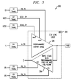
- FIG. 3 depicts at least a portion of an illustrative bidirectional buffer circuit 300 in which techniques of the present invention may be implemented.
- the buffer circuit 300 like buffer circuit 200 shown in FIG. 2 , may be divided into at least two functional circuit portions, namely, an input stage 304 and a programmable output stage 306 , although the buffer circuit may comprise other circuitry as well.
- buffer circuit 300 is more complex compared to buffer circuit 200 shown in FIG.
- buffer circuit 300 utilizes, in addition to enable signal EN and input signal A (utilized by buffer circuit 200 ), control signals PU, PD, OSC 1 and OSC 2 . It is to be understood that the invention is not limited to any particular number of signals utilized by the bidirectional buffer circuit 300 .
- IO buffer 302 operates in a higher IO signal domain (e.g., 3.3-volt), similar to IO buffer 202 depicted in FIG. 2 , and signals EN, OSC 1 , OSC 2 , A, PD and PU are typically generated by core logic circuitry operating in a lower core signal domain (e.g., 1.0-volt).
- Programmable output stage 306 may be operative in one of four different logic states controlled by signals OSC 1 and OSC 2 . These states may represent different operating characteristics of output stage 306 , such as, for example, different output impedances, slew rates, etc. For a programmable output stage that is operative in more than four logic states (e.g., 8), a greater number of control signals (e.g., 3) is required.
- input stage 304 may include programmable pull-up and pull-down devices.
- These pull-up and pull-down devices may comprise, for example, high impedance (e.g., about 50 kilo (K) ohms or higher) resistors, or alternative resistance elements (e.g., MOS device), that are controlled by signals PU and PD, respectively.
- K kilo
- MOS device alternative resistance elements
- the use of pull-up and pull-down resistors is often necessary in order to place input stage 304 in a known state when output stage 306 is in a high impedance state and no other buffer is driving the PAD node.
- bidirectional buffer circuit 300 further includes multiple voltage level translator circuits (TRANU) X 1 , X 2 , X 3 , X 4 , X 5 and X 6 .
- Voltage level translator circuit X 1 is operative to receive enable signal EN referenced to the lower core voltage supply and to generate a translated enable signal EN_ 3 V which is referenced to the higher IO voltage supply.
- voltage level translator circuit X 2 is operative to receive control signal OSC 1 referenced to the lower core voltage supply and to generate a translated control signal OSC 1 _ 3 V which is referenced to the higher IO voltage supply;
- voltage level translator circuit X 3 is operative to receive control signal OSC 2 referenced to the lower core voltage supply and to generate a translated control signal OSC 2 _ 3 V which is referenced to the higher IO voltage supply;
- voltage level translator circuit X 4 is operative to receive input signal A referenced to the lower core voltage supply and to generate a translated input signal A_ 3 V which is referenced to the higher IO voltage supply;
- voltage level translator circuit X 5 is operative to receive control signal PD referenced to the lower core voltage supply and to generate a translated control signal PD_ 3 V which is referenced to the higher IO voltage supply;
- voltage level translator circuit X 6 is operative to receive control signal PU referenced to the lower core voltage supply and to generate a translated control signal PU_ 3 V which is referenced to the higher IO
- buffer circuit 300 will be relatively large in comparison to buffer circuits which utilize a smaller number of control signals.
- two or more control signals may be advantageously multiplexed so as to share a single voltage level translator circuit.
- embodiments of the invention exploit the notion that certain signals which have an effect on one or more portions the IO buffer 302 during a first mode of operation of the buffer circuit 300 have substantially no effect on one or more other portions of the IO buffer during a second mode of operation of the buffer circuit.
- the IO buffer 302 is not utilized as both an input buffer and an output buffer concurrently, only the input stage 304 or the output stage 306 is active at any given time. When inactive, the respective logic states of the signals presented to a given input or output stage in the IO buffer are effectively irrelevant.
- signals OCS 1 and OCS 2 which are used to control a logic state of output stage 306 have no significant effect on the output stage if applied to the pull-down (pd) and pull-up (pu) control inputs of input stage 304 when the IO buffer is operative in an output mode.
- output stage 306 is preferably configured to drive the PAD node regardless of the state of the pull-up and pull-down devices in the input stage 304 .
- signals PU and PD which are used to control pull-up and pull-down devices, respectively, in input stage 304 have substantially no effect on the input stage if applied to the control inputs, ocs 1 and ocs 2 , of output stage 306 when the output stage is disabled (e.g., when IO buffer 302 is in an input mode).
- FIG. 4 is a schematic diagram depicting at least a portion of an exemplary bidirectional buffer circuit 400 , formed in accordance with an embodiment of the present invention.
- buffer circuit 400 may be similar to buffer circuit 300 shown in FIG. 3 , with one exception being that buffer circuit 400 has fewer voltage level translator circuits for the same number of signals presented to the buffer circuit.
- buffer circuit 400 preferably includes an IO buffer 302 which is divided into two functional sub-circuits, namely, an input stage 304 and a programmable output stage 306 , although the buffer circuit may comprise other circuitry in place of or in addition to the input and output stages.
- IO buffer 302 operates in a higher IO signal domain (e.g., 3.3-volt) and signals EN, OSC 1 , OSC 2 , A, PD and PU supplied to the buffer circuit 400 are typically generated by core logic circuitry operating in a lower core signal domain (e.g., 1.0-volt).
- buffer circuit 400 is operative to receive six signals, namely, signals EN, OSC 1 , OSC 2 , A, PD and PU
- buffer circuit 400 includes only four voltage level translator circuits (TRANUs), X 1 , X 2 , X 3 and X 4
- buffer circuit 300 depicted in FIG. 3 requires six voltage level translator circuits. It is to be appreciated, however, that the invention is not limited to any particular number of voltage level translator circuits or signals presented to the buffer circuit.
- Voltage level translator circuit X 1 is operative to receive enable signal EN referenced to the lower core voltage supply and to generate a translated enable signal EN_ 3 V which is referenced to the higher IO voltage supply.
- voltage level translator circuit X 4 is operative to receive input signal A referenced to the lower core voltage supply and to generate a translated input signal A_ 3 V which is referenced to the higher IO voltage supply.
- voltage level translator circuits X 1 and X 4 preferably function in a manner consistent with that described above in connection with FIG. 3 .
- Voltage level translator circuits X 2 and X 3 are each operative to receive one of two or more multiplexed signals to thereby reduce the number of voltage level translator circuits required by buffer circuit 400 .
- buffer circuit 400 includes first and second multiplexers (MUXs), XM 1 and XM 2 , respectively, or alternative control circuitry.
- MUXs multiplexers
- one or both multiplexers may comprise at least one pass gate (e.g., NMOS and/or PMOS device) connected in a conventional fashion, as will be understood by those skilled in the art.
- the multiplexers are typically significantly smaller in size compared to the voltage level translator circuits, which results in a beneficial reduction in chip area of buffer circuit 400 .
- XM 1 and XM 2 are depicted as two-input multiplexers, the invention is not limited to multiplexers of any particular number of inputs; nor is the invention limited to any particular number of multiplexers.
- Multiplexers XM 1 and XM 2 in conjunction with voltage level translator circuits X 1 through X 4 preferably form at least a portion of interface circuitry included in buffer circuit 400 .
- First multiplexer XM 1 is preferably operative to receive signals OSC 1 and PD referenced to the lower core voltage supply and to generate an output signal, N 1 , also referenced to the lower core supply.
- Signals OSC 1 and PD are preferably employed by buffer circuit 400 in mutually exclusive modes of operation of the buffer circuit.
- Output signal N 1 which is either signal OSC 1 or signal PD (or a respective signal indicative thereof) depending on the logical state of at least one control signal supplied to a control input of XM 1 , is then translated by voltage level translator circuit X 2 to generate a translated control signal SIG 1 _ 3 V which is referenced to the higher IO voltage supply.
- second multiplexer XM 2 is operative to receive signals OSC 2 and PU referenced to the lower core voltage supply and to generate an output signal, N 2 , also referenced to the lower core supply.
- Signals OSC 2 and PU are preferably employed by buffer circuit 400 in mutually exclusive modes of operation of the buffer circuit.
- Output signal N 2 which is either signal OSC 2 or signal PU (or a respective signal indicative thereof) depending on the logical state of at least one control signal supplied to a control input of XM 2 , is then translated by voltage level translator circuit X 3 to generate translated control signal SIG 2 _ 3 V which is referenced to the higher IO voltage supply.
- enable signal EN is preferably used as the control signal for multiplexers XM 1 and XM 2 , although an alternative control signal may be employed. It is convenient to use the enable signal EN since this signal is already employed by the buffer circuit 400 to control a mode of operation of the buffer circuit. For example, when signal EN is a logic high level, IO buffer 302 will preferably be operative in an output mode functioning as an output buffer, with output stage 306 being enabled. Conversely, when signal EN is a logic low level, IO buffer 302 is preferably operative in an input mode functioning as an input buffer, with output stage 306 being disabled (e.g., in a high-impedance state).
- control signals OSC 1 and OSC 2 are utilized to select the state of the output stage 306 , as previously explained. Therefore, when signal EN is high, multiplexers XM 1 and XM 2 are preferably configured such that signals OSC 1 and OSC 2 are selected as the output signals N 1 and N 2 , respectively.
- the voltage level translated signals SIG 1 _ 3 V and SIG 2 _ 3 V are fed to both input stage 304 and output stage 306 .
- the output signal Z generated by the input stage 304 is not used, and therefore these control signals SIG 1 _ 3 V and SIG 2 _ 3 V, when applied to the pd and pu control inputs, respectively, of the IO buffer, will have essentially no effect.
- control signals PD and PU are utilized by the IO buffer 302 to control the pull-down and pull-up devices, respectively, in input stage 304 , as previously stated.
- multiplexers XM 1 and XM 2 are preferably configured such that signals PD and PU are selected as the output signals N 1 and N 2 , respectively.
- the voltage level translated signals SIG 1 _ 3 V and SIG 2 _ 3 V are fed to both input stage 304 and output stage 306 .
- output stage 306 is disabled, and therefore these control signals SIG 1 _ 3 V and SIG 2 _ 3 V which drive the pull-up and pull-down devices, respectively, in input stage 304 will have essentially no effect on output stage 306 .
- the effective logical combination (e.g., logical AND, OR, etc.) of these signals can be used as the control signal for the multiplexers XM 1 and XM 2 .
- the bidirectional buffer circuit may include a circuit operative to drive pull-up and pull-down nodes in the input stage low while the IO buffer is operative in the output mode. This will ensure minimal leakage current in output mode.
- one or more functional blocks in buffer circuit 400 may be combined, either with one another or with one or more other functional blocks.
- FIG. 5 is a schematic diagram depicting at least a portion of an illustrative voltage level translator circuit 500 including multiplexed inputs, formed in accordance with another embodiment of the invention.
- Voltage level translator circuit 500 includes core voltage level translation circuitry 502 which is powered by a higher supply voltage (e.g., 3.3 volts), which may be VDD 33 , and receives, as its negative voltage supply, VSS, or an alternative current return (e.g., ground).
- Voltage level translation circuitry 502 may be implemented in a manner consistent with voltage level translator circuit 100 shown in FIG. 1 .
- Voltage level translation circuitry 502 preferably comprises a pair of high voltage PMOS transistor devices, M 3 P 1 and M 3 P 2 , connected in a cross-coupled configuration. Specifically, sources of M 3 P 1 and M 3 P 2 are connected to VDD 33 , a gate of M 3 P 1 is connected to a drain of M 3 P 2 at node N 1 , and a gate of M 3 P 2 is connected to a drain of M 3 P 1 at node N 2 . Voltage level translation circuitry 502 further includes an input stage comprising a pair of high voltage NMOS transistor devices, M 3 N 1 and M 3 N 2 , each device having a gate for receiving one of input multiplexed signals MXON and MXO, respectively.
- Sources of devices M 3 N 1 and M 3 N 2 are preferably connected to VSS, and drains of M 3 N 1 and M 3 N 2 are connected to the drains of PMOS transistors M 3 P 1 and M 3 P 2 , respectively.
- An output stage comprising high voltage PMOS transistor M 3 P 3 and high voltage NMOS transistor M 3 N 3 connected together as a standard inverter, is preferably connected to node N 1 and generates an output signal Z of the voltage level translator circuitry 502 at node N 3 .
- Voltage level translator circuit 500 further includes a multiplexer 504 which is operative to receive at least two signals, I 1 and I 2 , that are supplied to the circuit and to select, as an output of the multiplexer at node N 4 , one of signals I 1 and I 2 as a function of a control signal, S 1 , presented to the voltage level translator circuit.
- Multiplexer 504 preferably comprises a pair of complementary pass gates.
- a first pass gate includes a first low voltage PMOS transistor device M 1 P 1 and a first low voltage NMOS transistor device M 1 N 1 connected in parallel with one another.
- Sources of M 1 P 1 and M 1 N 1 are connected together and form a first input of the voltage level translator circuit 500 for receiving signal I 1 , drains of M 1 P 1 and M 1 N 1 are connected together at node N 4 , a gate of M 1 N 1 receives control signal S 1 , and a gate of M 1 P 1 receives signal S 1 N, a logical complement of signal S 1 .
- a second pass gate includes a second low voltage PMOS transistor device M 1 P 2 and a second low voltage NMOS transistor device M 1 N 2 connected in parallel with one another.
- Sources of M 1 P 2 and M 1 N 2 are connected together and form a second input of the voltage level translator circuit 500 for receiving signal I 2 , drains of M 1 P 2 and M 1 N 2 are connected together at node N 4 , a gate of M 1 N 2 receives control signal S 1 N, and a gate of M 1 P 2 receives signal S 1 .
- control signal S 1 When control signal S 1 is a logic high level, the first pass gate will be enabled and signal I 1 will be generated as the output of multiplexer 504 at node N 4 ; the second pass gate will be disabled.
- the output signal from multiplexer 504 will also be referenced to the lower core supply.
- signal S 1 is a logic low level
- the second pass gate When signal S 1 is a logic low level, the second pass gate will be enabled and signal I 2 will be generated as the output of multiplexer 504 at node N 4 ; the first pass gate will be disabled.
- the input signal MXO, and its logical complement signal MXON, are generated by a pair of inverters, INV 2 and INV 1 , respectively.
- Signal MXO is essentially a buffered version of the output of multiplexer 504 at node N 4 .
- FIG. 6 is a schematic diagram depicting at least a portion of an exemplary buffer circuit 600 , formed in accordance with another embodiment of the invention.
- buffer circuit 600 includes an output buffer array 602 which essentially replaces the IO buffer 302 in buffer circuit 400 shown in FIG. 4 .
- the output buffer array 602 in buffer circuit 600 comprises first and second output buffers, BUF 1 and BUF 2 , respectively, although this embodiment of the invention is not limited to the particular number of buffers shown.
- the output buffers BUF 1 and BUF 2 are connected together in parallel, such that an input of first output buffer BUF 1 is connected to an input of second output buffer BUF 2 at node N 1 , and an output of BUF 1 is connected to an output of BUF 2 at node N 2 .
- Buffers BUF 1 and BUF 2 may be the same or different.
- buffer BUF 1 may have a greater output drive capability compared to buffer BUF 2 .
- Buffers BUF 1 and BUF 2 are preferably configured such that when one buffer is enabled, the other is disabled (e.g., tri-stated) as a function of an enable signal, EN, or other control signal, supplied to the buffer circuit 600 .
- output buffer BUF 1 is enabled and output buffer BUF 2 is disabled.
- BUF 2 is enabled and BUF 1 is disabled.
- First output buffer BUF 1 receives an enable signal, EN_ 3 V
- second output buffer BUF 2 receives a logical complement of the enable signal, namely, signal ENB_ 3 V.
- signal EN_ 3 V is a logic high level
- BUF 1 is preferably enabled.
- Signal ENB_ 3 V being a logical complement of signal EN_ 3 V, will be a logic low level, thereby BUF 2 will be disabled, such as, for example, by placing the output of BUF 2 in a high-impedance state (e.g., tri-state). When disabled, the output of BUF 2 is preferably unaffected by signals applied to the input of BUF 2 . Conversely, when signal EN_ 3 V is a logic low level, BUF 1 is disabled, such as, for example, by placing the output of BUF 1 in a high-impedance state (e.g., tri-state). Signal ENB_ 3 V, being a logical complement of signal EN_ 3 V, will be a logic high level, thereby enabling BUF 2 . When disabled, the output of BUF 1 is preferably unaffected by signals applied to the input of BUF 1 .
- Each of the output buffers BUF 1 and BUF 2 are preferably connected to an IO voltage supply and are therefore operative in a higher IO signal domain (e.g., 3.3-volt).
- buffer circuit 600 is operative to receive signals, namely, signals A, B and EN, that are referenced to a core voltage supply, as may be generated by core logic, in a lower core signal domain (e.g., 1.0-volt). Consequently, these signals require voltage level translation to be compatible for use with output buffer array 602 .
- buffer circuit 600 includes a first voltage level translator circuit (TRANU) 604 operative to receive the enable signal EN and to generate signal EN_ 3 V, which is a voltage level-translated signal corresponding to signal EN.
- Voltage level translator circuit 604 may be implemented as shown in FIG. 1 and described above, although alternative voltage level translator circuit arrangements may be employed, as will be apparent to those skilled in the art.
- Buffer circuit 600 further includes a second voltage level translator circuit 606 that is operative to receive a signal, IN, which corresponds to one of input signals A and B referenced to the lower core supply, and to generate signal IN_ 3 V, which is a voltage level-translated signal corresponding to signal IN.
- voltage level translator circuits 604 and 606 may be different.
- a multiplexer (MUX) 608 included in buffer circuit 600 is preferably operative to receive input signals A and B referenced to the lower core voltage supply and to select, as an output of the MUX, one of input signals A and B as a function of a control signal supplied to the MUX.
- the control signal applied to MUX 608 is preferably the enable signal EN used for selectively controlling the mode of operation of buffer array 602 .
- a voltage level translator circuit can be eliminated, thereby beneficially reducing the area required by buffer circuit 600 .
- This unique multiplexing technique can be expanded, in accordance with other embodiments of the invention, to provide further beneficial reductions in chip area for more complex buffer circuits
- At least a portion of the bidirectional buffer circuit of the present invention may be implemented in an integrated circuit.
- identical die are typically fabricated in a repeated pattern on a surface of a semiconductor wafer.
- Each die includes a device described herein, and may include other structures and/or circuits.
- the individual die are cut or diced from the wafer, then packaged as an integrated circuit.
- One skilled in the art would know how to dice wafers and package die to produce integrated circuits. Integrated circuits so manufactured are considered part of this invention.
Landscapes
- Engineering & Computer Science (AREA)
- Computer Hardware Design (AREA)
- Physics & Mathematics (AREA)
- Computing Systems (AREA)
- General Engineering & Computer Science (AREA)
- Mathematical Physics (AREA)
- Logic Circuits (AREA)
Abstract
Description
Claims (18)
Priority Applications (1)
| Application Number | Priority Date | Filing Date | Title |
|---|---|---|---|
| US11/691,590 US7498860B2 (en) | 2007-03-27 | 2007-03-27 | Buffer circuit having multiplexed voltage level translation |
Applications Claiming Priority (1)
| Application Number | Priority Date | Filing Date | Title |
|---|---|---|---|
| US11/691,590 US7498860B2 (en) | 2007-03-27 | 2007-03-27 | Buffer circuit having multiplexed voltage level translation |
Publications (2)
| Publication Number | Publication Date |
|---|---|
| US20080238399A1 US20080238399A1 (en) | 2008-10-02 |
| US7498860B2 true US7498860B2 (en) | 2009-03-03 |
Family
ID=39793151
Family Applications (1)
| Application Number | Title | Priority Date | Filing Date |
|---|---|---|---|
| US11/691,590 Active US7498860B2 (en) | 2007-03-27 | 2007-03-27 | Buffer circuit having multiplexed voltage level translation |
Country Status (1)
| Country | Link |
|---|---|
| US (1) | US7498860B2 (en) |
Cited By (6)
| Publication number | Priority date | Publication date | Assignee | Title |
|---|---|---|---|---|
| US20130282844A1 (en) * | 2012-04-23 | 2013-10-24 | Contact Solutions LLC | Apparatus and methods for multi-mode asynchronous communication |
| US9166881B1 (en) | 2014-12-31 | 2015-10-20 | Contact Solutions LLC | Methods and apparatus for adaptive bandwidth-based communication management |
| US9218410B2 (en) | 2014-02-06 | 2015-12-22 | Contact Solutions LLC | Systems, apparatuses and methods for communication flow modification |
| US9635067B2 (en) | 2012-04-23 | 2017-04-25 | Verint Americas Inc. | Tracing and asynchronous communication network and routing method |
| US9641684B1 (en) | 2015-08-06 | 2017-05-02 | Verint Americas Inc. | Tracing and asynchronous communication network and routing method |
| US10063647B2 (en) | 2015-12-31 | 2018-08-28 | Verint Americas Inc. | Systems, apparatuses, and methods for intelligent network communication and engagement |
Families Citing this family (4)
| Publication number | Priority date | Publication date | Assignee | Title |
|---|---|---|---|---|
| CN111984575B (en) * | 2019-05-24 | 2021-12-17 | 瑞昱半导体股份有限公司 | Signal transmission circuit and method |
| FR3106708B1 (en) * | 2020-01-24 | 2024-06-14 | St Microelectronics Rousset | INTEGRATED CONDITIONING CIRCUIT |
| KR102828952B1 (en) * | 2020-04-06 | 2025-07-04 | 에스케이하이닉스 주식회사 | Memory apparatus having a structure coupling a pad and a circuit |
| US11791824B1 (en) * | 2022-05-11 | 2023-10-17 | Apple Inc. | Voltage domain GPIO control |
Citations (2)
| Publication number | Priority date | Publication date | Assignee | Title |
|---|---|---|---|---|
| US6480026B2 (en) * | 2000-05-26 | 2002-11-12 | Lattice Semiconductor Corporation | Multi-functional I/O buffers in a field programmable gate array (FPGA) |
| US6856173B1 (en) * | 2003-09-05 | 2005-02-15 | Freescale Semiconductor, Inc. | Multiplexing of digital signals at multiple supply voltages in an integrated circuit |
-
2007
- 2007-03-27 US US11/691,590 patent/US7498860B2/en active Active
Patent Citations (2)
| Publication number | Priority date | Publication date | Assignee | Title |
|---|---|---|---|---|
| US6480026B2 (en) * | 2000-05-26 | 2002-11-12 | Lattice Semiconductor Corporation | Multi-functional I/O buffers in a field programmable gate array (FPGA) |
| US6856173B1 (en) * | 2003-09-05 | 2005-02-15 | Freescale Semiconductor, Inc. | Multiplexing of digital signals at multiple supply voltages in an integrated circuit |
Cited By (13)
| Publication number | Priority date | Publication date | Assignee | Title |
|---|---|---|---|---|
| US10015263B2 (en) | 2012-04-23 | 2018-07-03 | Verint Americas Inc. | Apparatus and methods for multi-mode asynchronous communication |
| WO2013163169A1 (en) * | 2012-04-23 | 2013-10-31 | Contact Solutions, Llc | Apparatus and methods for multi-mode asynchronous communication |
| US8880631B2 (en) | 2012-04-23 | 2014-11-04 | Contact Solutions LLC | Apparatus and methods for multi-mode asynchronous communication |
| GB2520175A (en) * | 2012-04-23 | 2015-05-13 | Contact Solutions LLC | Apparatus and methods for multi-mode asynchronous communication |
| US9172690B2 (en) | 2012-04-23 | 2015-10-27 | Contact Solutions LLC | Apparatus and methods for multi-mode asynchronous communication |
| US9635067B2 (en) | 2012-04-23 | 2017-04-25 | Verint Americas Inc. | Tracing and asynchronous communication network and routing method |
| US20130282844A1 (en) * | 2012-04-23 | 2013-10-24 | Contact Solutions LLC | Apparatus and methods for multi-mode asynchronous communication |
| US9218410B2 (en) | 2014-02-06 | 2015-12-22 | Contact Solutions LLC | Systems, apparatuses and methods for communication flow modification |
| US10506101B2 (en) | 2014-02-06 | 2019-12-10 | Verint Americas Inc. | Systems, apparatuses and methods for communication flow modification |
| US9166881B1 (en) | 2014-12-31 | 2015-10-20 | Contact Solutions LLC | Methods and apparatus for adaptive bandwidth-based communication management |
| US9641684B1 (en) | 2015-08-06 | 2017-05-02 | Verint Americas Inc. | Tracing and asynchronous communication network and routing method |
| US10063647B2 (en) | 2015-12-31 | 2018-08-28 | Verint Americas Inc. | Systems, apparatuses, and methods for intelligent network communication and engagement |
| US10848579B2 (en) | 2015-12-31 | 2020-11-24 | Verint Americas Inc. | Systems, apparatuses, and methods for intelligent network communication and engagement |
Also Published As
| Publication number | Publication date |
|---|---|
| US20080238399A1 (en) | 2008-10-02 |
Similar Documents
| Publication | Publication Date | Title |
|---|---|---|
| US7498860B2 (en) | Buffer circuit having multiplexed voltage level translation | |
| EP1024597B1 (en) | Output circuit for use in a semiconductor integrated circuit | |
| US7038516B2 (en) | Current-controlled CMOS logic family | |
| US8362803B2 (en) | Mode latching buffer circuit | |
| JP4417552B2 (en) | High speed ratio type CMOS logic structure for pulse input | |
| EP0099100A1 (en) | Gate circuit of combined field-effect and bipolar transistors | |
| JP3079009B2 (en) | Mixed voltage output buffer circuit | |
| KR20110119620A (en) | Voltage converter circuits, buffer circuits, integrated circuits and electronic systems | |
| JPH08237102A (en) | I / O buffer circuit device | |
| JPH09246942A (en) | Semiconductor output circuit | |
| US10840892B1 (en) | Fully digital, static, true single-phase clock (TSPC) flip-flop | |
| US6803789B1 (en) | High voltage tolerant output buffer | |
| US5907249A (en) | Voltage tolerant input/output buffer | |
| US6249146B1 (en) | MOS output buffer with overvoltage protection circuitry | |
| US6373291B1 (en) | Pass transistor logic circuit for reducing power consumption | |
| US7382168B2 (en) | Buffer circuit with multiple voltage range | |
| US5880617A (en) | Level conversion circuit and semiconductor integrated circuit | |
| US6577163B1 (en) | Configurable PCI clamp or high voltage tolerant I/O circuit | |
| JP3672184B2 (en) | Macro cell for relay | |
| US6496054B1 (en) | Control signal generator for an overvoltage-tolerant interface circuit on a low voltage process | |
| KR20010108290A (en) | Methods and apparatus for bipolar elimination in silicon-on-insulator(soi) domino circuits | |
| US6232819B1 (en) | Semiconductor integrated circuit device and low-amplitude signal receiving method | |
| US5398000A (en) | Simple and high speed BICMOS tristate buffer circuit | |
| US7420403B2 (en) | Latch circuit and flip-flop | |
| US20030151428A1 (en) | 5 Volt tolerant input/output buffer |
Legal Events
| Date | Code | Title | Description |
|---|---|---|---|
| AS | Assignment |
Owner name: AGERE SYSTEMS INC., PENNSYLVANIA Free format text: ASSIGNMENT OF ASSIGNORS INTEREST;ASSIGNORS:BHATTACHARYA, DIPANKAR;HUBER, CAROL A.;KOTHANDARAMAN, MAKESHWAR;AND OTHERS;REEL/FRAME:019068/0632 Effective date: 20070326 |
|
| AS | Assignment |
Owner name: GENERAL ELECTRIC COMPANY, NEW YORK Free format text: ASSIGNMENT OF ASSIGNORS INTEREST;ASSIGNORS:BANSAL, VISHAL;DUONG, HIEU MINH;REEL/FRAME:019095/0173;SIGNING DATES FROM 20070327 TO 20070329 |
|
| STCF | Information on status: patent grant |
Free format text: PATENTED CASE |
|
| FPAY | Fee payment |
Year of fee payment: 4 |
|
| AS | Assignment |
Owner name: DEUTSCHE BANK AG NEW YORK BRANCH, AS COLLATERAL AGENT, NEW YORK Free format text: PATENT SECURITY AGREEMENT;ASSIGNORS:LSI CORPORATION;AGERE SYSTEMS LLC;REEL/FRAME:032856/0031 Effective date: 20140506 Owner name: DEUTSCHE BANK AG NEW YORK BRANCH, AS COLLATERAL AG Free format text: PATENT SECURITY AGREEMENT;ASSIGNORS:LSI CORPORATION;AGERE SYSTEMS LLC;REEL/FRAME:032856/0031 Effective date: 20140506 |
|
| AS | Assignment |
Owner name: AVAGO TECHNOLOGIES GENERAL IP (SINGAPORE) PTE. LTD., SINGAPORE Free format text: ASSIGNMENT OF ASSIGNORS INTEREST;ASSIGNOR:AGERE SYSTEMS LLC;REEL/FRAME:035365/0634 Effective date: 20140804 Owner name: AVAGO TECHNOLOGIES GENERAL IP (SINGAPORE) PTE. LTD Free format text: ASSIGNMENT OF ASSIGNORS INTEREST;ASSIGNOR:AGERE SYSTEMS LLC;REEL/FRAME:035365/0634 Effective date: 20140804 |
|
| AS | Assignment |
Owner name: LSI CORPORATION, CALIFORNIA Free format text: TERMINATION AND RELEASE OF SECURITY INTEREST IN PATENT RIGHTS (RELEASES RF 032856-0031);ASSIGNOR:DEUTSCHE BANK AG NEW YORK BRANCH, AS COLLATERAL AGENT;REEL/FRAME:037684/0039 Effective date: 20160201 Owner name: AGERE SYSTEMS LLC, PENNSYLVANIA Free format text: TERMINATION AND RELEASE OF SECURITY INTEREST IN PATENT RIGHTS (RELEASES RF 032856-0031);ASSIGNOR:DEUTSCHE BANK AG NEW YORK BRANCH, AS COLLATERAL AGENT;REEL/FRAME:037684/0039 Effective date: 20160201 |
|
| AS | Assignment |
Owner name: BANK OF AMERICA, N.A., AS COLLATERAL AGENT, NORTH CAROLINA Free format text: PATENT SECURITY AGREEMENT;ASSIGNOR:AVAGO TECHNOLOGIES GENERAL IP (SINGAPORE) PTE. LTD.;REEL/FRAME:037808/0001 Effective date: 20160201 Owner name: BANK OF AMERICA, N.A., AS COLLATERAL AGENT, NORTH Free format text: PATENT SECURITY AGREEMENT;ASSIGNOR:AVAGO TECHNOLOGIES GENERAL IP (SINGAPORE) PTE. LTD.;REEL/FRAME:037808/0001 Effective date: 20160201 |
|
| FPAY | Fee payment |
Year of fee payment: 8 |
|
| AS | Assignment |
Owner name: AVAGO TECHNOLOGIES GENERAL IP (SINGAPORE) PTE. LTD., SINGAPORE Free format text: TERMINATION AND RELEASE OF SECURITY INTEREST IN PATENTS;ASSIGNOR:BANK OF AMERICA, N.A., AS COLLATERAL AGENT;REEL/FRAME:041710/0001 Effective date: 20170119 Owner name: AVAGO TECHNOLOGIES GENERAL IP (SINGAPORE) PTE. LTD Free format text: TERMINATION AND RELEASE OF SECURITY INTEREST IN PATENTS;ASSIGNOR:BANK OF AMERICA, N.A., AS COLLATERAL AGENT;REEL/FRAME:041710/0001 Effective date: 20170119 |
|
| AS | Assignment |
Owner name: AVAGO TECHNOLOGIES INTERNATIONAL SALES PTE. LIMITED, SINGAPORE Free format text: MERGER;ASSIGNOR:AVAGO TECHNOLOGIES GENERAL IP (SINGAPORE) PTE. LTD.;REEL/FRAME:047195/0827 Effective date: 20180509 Owner name: AVAGO TECHNOLOGIES INTERNATIONAL SALES PTE. LIMITE Free format text: MERGER;ASSIGNOR:AVAGO TECHNOLOGIES GENERAL IP (SINGAPORE) PTE. LTD.;REEL/FRAME:047195/0827 Effective date: 20180509 |
|
| AS | Assignment |
Owner name: AVAGO TECHNOLOGIES INTERNATIONAL SALES PTE. LIMITED, SINGAPORE Free format text: CORRECTIVE ASSIGNMENT TO CORRECT THE EFFECTIVE DATE OF MERGER PREVIOUSLY RECORDED AT REEL: 047195 FRAME: 0827. ASSIGNOR(S) HEREBY CONFIRMS THE MERGER;ASSIGNOR:AVAGO TECHNOLOGIES GENERAL IP (SINGAPORE) PTE. LTD.;REEL/FRAME:047924/0571 Effective date: 20180905 Owner name: AVAGO TECHNOLOGIES INTERNATIONAL SALES PTE. LIMITE Free format text: CORRECTIVE ASSIGNMENT TO CORRECT THE EFFECTIVE DATE OF MERGER PREVIOUSLY RECORDED AT REEL: 047195 FRAME: 0827. ASSIGNOR(S) HEREBY CONFIRMS THE MERGER;ASSIGNOR:AVAGO TECHNOLOGIES GENERAL IP (SINGAPORE) PTE. LTD.;REEL/FRAME:047924/0571 Effective date: 20180905 |
|
| MAFP | Maintenance fee payment |
Free format text: PAYMENT OF MAINTENANCE FEE, 12TH YEAR, LARGE ENTITY (ORIGINAL EVENT CODE: M1553); ENTITY STATUS OF PATENT OWNER: LARGE ENTITY Year of fee payment: 12 |