US7479672B2 - Power junction field effect power transistor with highly vertical channel and uniform channel opening - Google Patents
Power junction field effect power transistor with highly vertical channel and uniform channel opening Download PDFInfo
- Publication number
- US7479672B2 US7479672B2 US11/784,613 US78461307A US7479672B2 US 7479672 B2 US7479672 B2 US 7479672B2 US 78461307 A US78461307 A US 78461307A US 7479672 B2 US7479672 B2 US 7479672B2
- Authority
- US
- United States
- Prior art keywords
- vertical
- layer
- junction field
- effect transistor
- type
- Prior art date
- Legal status (The legal status is an assumption and is not a legal conclusion. Google has not performed a legal analysis and makes no representation as to the accuracy of the status listed.)
- Expired - Lifetime
Links
- 230000005669 field effect Effects 0.000 title claims abstract description 24
- 230000000903 blocking effect Effects 0.000 claims abstract description 33
- 239000004065 semiconductor Substances 0.000 claims abstract description 26
- 108091006146 Channels Proteins 0.000 claims description 103
- 238000005468 ion implantation Methods 0.000 claims description 20
- 239000002184 metal Substances 0.000 claims description 12
- 238000002161 passivation Methods 0.000 claims description 5
- 102000004129 N-Type Calcium Channels Human genes 0.000 claims description 3
- 108090000699 N-Type Calcium Channels Proteins 0.000 claims description 3
- 229910010271 silicon carbide Inorganic materials 0.000 description 29
- HBMJWWWQQXIZIP-UHFFFAOYSA-N silicon carbide Chemical compound [Si+]#[C-] HBMJWWWQQXIZIP-UHFFFAOYSA-N 0.000 description 23
- 238000002513 implantation Methods 0.000 description 14
- 230000004888 barrier function Effects 0.000 description 11
- 238000000034 method Methods 0.000 description 9
- 239000000370 acceptor Substances 0.000 description 8
- 230000006698 induction Effects 0.000 description 5
- 230000003068 static effect Effects 0.000 description 5
- 229920002120 photoresistant polymer Polymers 0.000 description 4
- 239000000758 substrate Substances 0.000 description 4
- 239000004642 Polyimide Substances 0.000 description 3
- 230000015572 biosynthetic process Effects 0.000 description 3
- 230000015556 catabolic process Effects 0.000 description 3
- 238000005530 etching Methods 0.000 description 3
- 229920001721 polyimide Polymers 0.000 description 3
- 235000012431 wafers Nutrition 0.000 description 3
- VYPSYNLAJGMNEJ-UHFFFAOYSA-N Silicium dioxide Chemical compound O=[Si]=O VYPSYNLAJGMNEJ-UHFFFAOYSA-N 0.000 description 2
- XUIMIQQOPSSXEZ-UHFFFAOYSA-N Silicon Chemical compound [Si] XUIMIQQOPSSXEZ-UHFFFAOYSA-N 0.000 description 2
- 210000000746 body region Anatomy 0.000 description 2
- 229910003460 diamond Inorganic materials 0.000 description 2
- 239000010432 diamond Substances 0.000 description 2
- 238000002347 injection Methods 0.000 description 2
- 239000007924 injection Substances 0.000 description 2
- 238000000623 plasma-assisted chemical vapour deposition Methods 0.000 description 2
- 229910052710 silicon Inorganic materials 0.000 description 2
- 239000010703 silicon Substances 0.000 description 2
- 229910002704 AlGaN Inorganic materials 0.000 description 1
- 229910002601 GaN Inorganic materials 0.000 description 1
- 229910001218 Gallium arsenide Inorganic materials 0.000 description 1
- -1 InGaN Inorganic materials 0.000 description 1
- 238000013459 approach Methods 0.000 description 1
- 229910052681 coesite Inorganic materials 0.000 description 1
- 229910052906 cristobalite Inorganic materials 0.000 description 1
- 230000003247 decreasing effect Effects 0.000 description 1
- 238000001312 dry etching Methods 0.000 description 1
- 230000000694 effects Effects 0.000 description 1
- 230000005684 electric field Effects 0.000 description 1
- 238000004519 manufacturing process Methods 0.000 description 1
- 239000000463 material Substances 0.000 description 1
- 229910003465 moissanite Inorganic materials 0.000 description 1
- 150000004767 nitrides Chemical class 0.000 description 1
- 238000005457 optimization Methods 0.000 description 1
- 230000003647 oxidation Effects 0.000 description 1
- 238000007254 oxidation reaction Methods 0.000 description 1
- 238000005036 potential barrier Methods 0.000 description 1
- 239000000377 silicon dioxide Substances 0.000 description 1
- 238000004088 simulation Methods 0.000 description 1
- 238000004528 spin coating Methods 0.000 description 1
- 229910052682 stishovite Inorganic materials 0.000 description 1
- 229910052905 tridymite Inorganic materials 0.000 description 1
Images


Classifications
-
- H—ELECTRICITY
- H10—SEMICONDUCTOR DEVICES; ELECTRIC SOLID-STATE DEVICES NOT OTHERWISE PROVIDED FOR
- H10D—INORGANIC ELECTRIC SEMICONDUCTOR DEVICES
- H10D30/00—Field-effect transistors [FET]
- H10D30/80—FETs having rectifying junction gate electrodes
- H10D30/83—FETs having PN junction gate electrodes
- H10D30/831—Vertical FETs having PN junction gate electrodes
-
- H—ELECTRICITY
- H10—SEMICONDUCTOR DEVICES; ELECTRIC SOLID-STATE DEVICES NOT OTHERWISE PROVIDED FOR
- H10D—INORGANIC ELECTRIC SEMICONDUCTOR DEVICES
- H10D62/00—Semiconductor bodies, or regions thereof, of devices having potential barriers
- H10D62/10—Shapes, relative sizes or dispositions of the regions of the semiconductor bodies; Shapes of the semiconductor bodies
- H10D62/17—Semiconductor regions connected to electrodes not carrying current to be rectified, amplified or switched, e.g. channel regions
- H10D62/343—Gate regions of field-effect devices having PN junction gates
Definitions
- This invention relates to the creation and design of power semiconductor switches. More specifically, this invention relates to vertical junction field-effect power transistors with long vertical channels all having a highly uniform channel opening dimension defined and controlled by highly vertical p + n junctions.
- FIG. 1 is a copy of FIG. 6A from U.S. Pat. No. 6,107,649.
- FIG. 6 a copy of FIG. 1 in the paper by J. Nishizawa et al.
- SIT and VJFET gates formed by normal incident ion implantation generally lead to highly non-uniform channel opening dimensions similar to the curved channel of FIG. 7 .
- the channel is near 2 um, the vertical part of the channel that has the same channel opening dimension is negligible in comparison to the total channel length.
- the vertical JFET blocks only 2 kV, much below the theoretical blocking voltage limit of >3 kV for the 20 um thick structure shown in FIG. 7 because of the absence of a long vertical channel with a highly uniform channel opening dimension.
- the device specific on-resistance is as high as 70 m ⁇ cm 2 .
- the vertical JFET is a normally-on switch, again due to the absence of long vertical channel with a highly uniform opening dimension defined and controlled to be normally-off by highly vertical p + n junctions.
- pure vertical JFETs with gate junctions formed by normal incident ion implantation without long vertical channels of a highly uniform channel opening dimension are not desirable for the implementation of normally-off operation. It is also obvious to those skilled in the art that pure vertical JFETs can not offer optimum normally-on operation when the gate junctions are formed by normal incident ion implantation without long vertical channels of a highly uniform channel opening dimension because an excessive negative gate bias is needed to create a barrier with enough depth to block desired voltages.
- VJFETs pure vertical JFETs
- the device includes a large number of paralleled cells fabricated on wafers with an n + -n ⁇ -n-n ++ structure, where the n ++ is the top source layer for the source ohmic contact and for defining the boundary of the vertical p + n junction gates remote from the top surface.
- the n ⁇ layer forms the drift or blocking layer.
- the n layer is the channel layer used to form the vertical mesas and vertical channels.
- the n- layer is for the blocking layer.
- the n + region is the bottom drain layer or substrate upon which the n ⁇ blocking layer, the n channel layer n and the n ++ source layer are grown.
- Each cell contains a highly vertical mesa defined by deep U-shaped trenches in the semiconductor with the center region of each mesa forming the long vertical channel of the cell.
- a U-shaped gate p + n junction is formed by angled or tilted ion implantation of acceptors whose energy controls the vertical channel opening dimension, resulting in a highly uniform vertical channel opening.
- Gate ohmic contacts are placed on the bottom of the U-shaped trenches on p ++ region selectively formed by ion implantation on the bottom of the U-shaped p + n junction.
- the trenches are planarized by a standard planarization technique such as spin-coating of polyimide.
- Source ohmic contacts are placed on the mesa surface of the n ++ top source layer.
- Drain ohmic contact is formed on the n + bottom surface of the bottom drain layer.
- the n ⁇ blocking layer and the n channel layer can be combined into a single n layer when separate optimization of the blocking and channel layers are not required.
- FIG. 1 shows prior art in the design of SiCVJFETs with lateral JFETs.
- FIG. 2 shows prior art in the design of SiC VJFETs with lateral JFETs.
- FIG. 3 shows prior art in the design of SiC static induction transistors (SIT s).
- FIG. 4 shows prior art in another design of SiC static induction transistors (SIT s).
- FIG. 5 shows prior art in yet another design of SiC static induction transistors (SITs).
- FIG. 6 shows prior art in the design of Si SITs.
- FIG. 7 shows prior art in the design of high voltage SiC VJFETs with long vertical channels.
- FIG. 8 shows a cross sectional view embodying one form of the invention.
- FIG. 8 a shows a three-dimensional cross section view of the embodiment shown in FIG. 8 .
- FIG. 9 shows cross sectional view of formation of a long vertical channel with a highly uniform channel opening dimension by titled ion implantation of acceptors using thick and heavily doped n ++ 0 source layer by a self-aligned process.
- FIG. 10 shows cross sectional view embodying another form of the invention.
- FIG. 11 shows the cross sectional view of a 4H—SiC VJFET designed and fabricated according to the invention using a single 7 ⁇ 10 15 cm ⁇ 3 doped n-type layer for the drift layer as well as the vertical channel n layer.
- FIG. 12 shows the experimental room temperature I-V curves for the fabricated 4H—SiC VJFET.
- FIG. 13 shows the cross sectional view of a design for a 14 kV SiC VJFET.
- FIG. 14 shows the simulated I-V curves for the 14 kV SiC VJFET designed.
- FIG. 8 with one embodiment of the VJFET where a four-layer semiconductor structure having top surface 155 and bottom surface 165 is used to fabricate the VJFET.
- the cross section of FIG. 8 corresponds to a unit cell of the VJFET.
- a complete VJFET is formed by repeating this unit cell resulting in a large number of cells in parallel.
- Two unit cells of the VJFET are visible in the three-dimensional cross section view shown in FIG. 8 .
- the bottom drain layer 20 is a heavily doped n + bulk semiconductor upon which the epilayers are grown.
- On top of layer 20 is first grown a lightly doped thick n ⁇ drift layer 40 followed by an n type channel layer 50 .
- n + buffer layer 30 can be used between layer 40 and substrate 20 .
- the thicknesses and doping concentrations for layers 40 and 50 are determined by the desired device voltage blocking capability and current requirement through well known device physics equations.
- an n ++ layer 60 with a doping density higher than that of the p + gate and with a thickness larger than the etch depth non-uniformity in photoresist (PR) and dielectric (such as polyimide) etch-back during a standard semiconductor planarization process.
- PR photoresist
- dielectric such as polyimide
- Layer 60 can also be formed by ion implantation of donors, such as P or N either at room temperature or at high temperatures.
- the device includes the drain ohmic contact 150 ; the vertical p+ gate 90 which, in this embodiment, is formed by first etching deep U-shaped trenches (regions) 85 to form mesas 65 with highly vertical ( ⁇ 90°) side walls. Each mesa is rectangular shaped and bounded on four sides by a U-shaped trench.
- FIG. 8 shows half of a U-shaped trench 85 to the left of mesa 65 and half of another U-shaped trench to the right of mesa 65 .
- a complete U-shaped trench 85 is shown between two mesas in FIG. 8A .
- the walls of the U-shaped trenches form the basis for U-shaped gate (p + n) junctions.
- tilted or angled acceptor ion implantation is applied to the four sides of the mesa walls with a density lower than the donor density of the top source n ++ layer 60 , which is typically 2 to 10 ⁇ 10 18 cm ⁇ 3 or higher, to form the highly vertical p+ gate 90 which surrounds each mesa 65 on four sides and defines a highly vertical channel 50 with a highly uniform channel opening dimension (d 0 );
- the p+ trench bottom region 70 (or p+ body region 70 ) typically doped in 10 18 cm ⁇ 3 range is formed by normal incident acceptor implantation;
- the p ++ selectively and heavily doped region of 80 which is for better gate ohmic contact formation and is formed together with region 70 but with increased acceptor dose near the surface region 95 ;
- the vertical depth of the trench and the vertical depth of the p + body implantation (region 70 ) together determine the length (L vc ) of the highly vertical part of the channel.
- the length of L vc should be designed to provide a negligible effect of the well know FET DIBL barrier lowering. It should be obvious to those skilled in the art that there is a trade-off in the blocking voltage and device resistance. A longer channel length L vc results in a larger channel resistance but a larger source-to-drain barrier, leading to a lower leakage current and a higher blocking voltage while a shorter channel length L vc results in a smaller channel resistance but a DIBL barrier lowering and a higher leakage current, leading to a lower blocking voltage.
- Lvc The exact optimum length of Lvc depends not only on the maximum blocking voltage but also on the maximum allowed leakage current between source and drain of the VJFET and the normally-off or normally-on mode of operation which are all governed by the well known semiconductor device equations.
- the desired tilted angle, the implantation energy and the dose of acceptors depend on the desired vertical channel opening dimension which is largely determined by the channel doping concentration and the gate p + n junction built-in voltage.
- the vertical channel opening should be completely depleted by the built-in voltages of the p + n junctions on each side the vertical channel.
- the vertical channel opening dimension can be controlled to very high accuracy in the submicron range, only limited by the masks used to define the source mesas.
- n ++ source layer 60 thick enough so that (i) self-aligned (by using metal on mesa as implantation mask) and tilted or angled implantation can be used to create p+ vertical side walls without converting any part of the top source layer 60 from n-type to p-type (as illustrated by FIG.
- the part of the n-type source layer subjected to acceptor implantation can be converted to p-type after the tilted, angled implantation to the vertical side walls of the mesa, making it very difficult to define the source ohmic contact without causing a short-circuit between the source contact metal 140 and the p + gate region 90 .
- n ++ source layer 60 even if the source layer is doped very heavily, it would also be very difficult to form the source contact 140 and the subsequent metal overlay 130 , without causing short-circuit between the source metal and the top of the p + gate.
- n ++ layer 60 should be thicker than the etch depth non-uniformity encountered in the photoresist (PR) and dielectric (such as polyimide) etch-back during a standard semiconductor planarization process.
- the etch depth non-uniformity in semiconductor planarization process varies, depending on equipment used and processes employed, but is generally within the range of 0.2 to 2 um although non-uniformity outside this range is also possible.
- a thick enough n ++ layer 60 would allow the use of self-aligned processes to define source ohmic metal contact 140 to the top of the mesa surface 150 , and to form a thick metal overlay 130 connecting all mesa tops without shorting the p + gate 90 and the n ++ source 60 .
- the VJFET of FIG. 8 operates by applying a high blocking voltage to the drain with respect to the source.
- the vertical channel is off when there is no gate-to-source bias.
- a reverse bias across the gate-to-source p + n ++ junction needs to be applied to turn-off the vertical channel.
- the reverse biased p + ( 70 )-n ⁇ ( 40 ) junction blocks the drain to source voltage.
- the depletion width around the vertical p+gate regions on either sides of the vertical channel 50 expands and substantially shields the source 60 .
- the maximum blocking voltage is therefore determined largely by the reverse biased p+-n ⁇ structure formed by the p + body region 70 and the n ⁇ blocking region 40 .
- a forward bias across the gate and source p + n ++ junction drives the device into the conduction mode by reducing the depletion width and opening up the vertical channel so that current conducts between the drain and source.
- the forward bias does not need to fully turn on the gate-to-source p + n + diode and the forward current going through the gate can be negligible in comparison to drain to source current.
- reducing the reverse bias across the gate-to-source pn junction would open up the vertical channel and lead to current conduction between the drain and source.
- this unipolar VJFET can also be operated in hybrid mode with a small quantity of hole injection by simply increasing the gate-to-source forward bias.
- the device is turned off after removing the gate-to-source bias in the case of normally-off VJFETs and after increasing the reverse gate-to-source bias to shut off the vertical channel in the case of normally-on VJFETs.
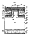
- FIG. 10 with another embodiment of the invention where a bipolar VJFET is disclosed.
- the difference between the embodiment of FIG. 10 and the embodiment of FIG. 8 is in the use of bottom drain layer and buffer layer with conductivity type opposite to that of the blocking layer in FIG. 10 .
- the bottom drain layer 220 in the specific illustration of FIG. 10 is a heavily doped p-type substrate.
- the buffer layer 230 shown in FIG. 10 is also a heavily doped p-type layer.
- the use of a bipolar drain junction results in a bipolar-mode VJFET which has a highly vertical channel with a highly uniform channel opening.
- the bipolar-VJFET is biased in the same way as a unipolar VJFET of FIG. 8 .
- the vertical channel is pinched off at zero (reverse) gate-to-source bias for normally-off (normally-on) VJFETs and the blocking voltage is supported by the reverse biased p + ( 270 )-n ⁇ ( 240 ) junction.
- an appropriate gate bias is applied to open up the vertical channel to allow current passing from the drain to the source. Because the drain-to-source is formed by a p + -n ⁇ n ++ structure in this bipolar VJFET instead of the n + -n ⁇ -n ++ structure in the unipolar VJFET, conductivity modulation due to hole injection into the thick n-type lightly doped blocking layer 240 will substantially reduce the device specific on-resistance.
- FIG. 11 shows the cross sectional view of a VJFET designed and fabricated according to the invention using a single 7 ⁇ 10 15 cm ⁇ 3 doped n-type layer for the drift layer as well as the vertical channel n layer.
- the length of the vertical part of the channel is designed to be 2.1 um and the channel opening dimension is highly uniform and is designed to be equal to 0.55 um.
- the top n ++ source contact layer is doped 1 ⁇ 10 19 cm ⁇ 3 with a large thickness of 1.6um so that self-aligned gate p + implantation can be done to form the vertical channel with a highly uniform channel opening dimension.
- the blocking layer thickness defined as the thickness of the n layer between the p+ body and n+ substrate is 9.4um when 0.2um p+ implantation tail is considered.
- the highly vertical channel is formed by first etching a deep trench of 3.2um, followed by tilted Al ion implantation onto all four sides of the mesas forming accurately controlled vertical channels of 2.1um in length and a highly uniform vertical channel opening dimension of 0.55um.
- the vertical channel length of 2.1um is the sum of 1.6um of the U-shaped trench depth and 0.5um of the p+ gate implantation depth.
- blocking layer doping density should be decreased and its thickness should be increased as well understood by those skilled in the art.
- FIG. 12 shows the experimental I-V curves for the fabricated VJFET measured at room temperature.
- FIG. 11 and FIG. 12 are copied from FIG. 1 and FIG.
- the VJFET is capable of a blocking voltage (V bl ) of 1,726V with a specific on-resistance (R sp ) of 3.6 m ⁇ cm 2 at a drain to source voltage of 3V and a gate-to-source bias of 5V, corresponding to a figure-of-merit of V bl 2 /R sp equal to 827MW/cm 2 which is the highest for any type of normally-off or normally-on SiC unipolar or bipolar power switches reported to date.
- V bl blocking voltage
- R sp specific on-resistance
- FIG. 13 shows the design of a 14 kV SiC VJFET and FIG. 14 shows the simulated I-V curves for the 14 kV SiC VJFET designed with the same 2.1 um vertical channel length of FIG. 11 , confirming that SiC VJFETs with up to 14 kV blocking voltage can be realized without changing the vertical channel length.
- FIG. 13 and FIG. 14 are copied from FIG. 8 and FIG. 9 in the paper by J. H. Zhao et al. published by IEEE ISPSD-2003, pp. 50-52.
- the vertical channels can be formed by epitaxial refilling of p+ SiC into the U-shaped trench regions to define the desired vertical channels with a highly uniform channel opening dimension.
- the conductivity type of each layer can be changed to the opposite type to form a VJFET.
- double-sided epitaxial growth or double-sided ion implantation onto both sides of a bulk wafer of an appropriate thickness in the range of 100 um to 400 um and a doping density in the range of 10 13 cm ⁇ 3 to 10 15 cm ⁇ 3 can be used to implement the invention.
- the vertical channel length while described as 2.1 um for up to 14 kV VJFETs, can be smaller in designing lower voltage VJFETs as described in a paper published by J. H. Zhao et al. entitled demonstration of a high performance 4 H—SiC vertical junction field effect transistor without epitaxial regrowth by IEE Electronics Letters, Vol. 39, No. 3, Feb. 6, 2003, pp. 321-323, cited here as reference, which reports an experimental normally-on VJFET blocking 392V achieving a very low R sp of 1.4 m ⁇ cm 2 using a vertical channel length of 1.57 um and a blocking layer of only 1.33 um.
- SiC semiconductor is used as example of illustration, other semiconductors can be equally used to form the VJFET of the invention such as GaN, AlGaN, InGaN, diamond, AlGaAsP, Si, ZnO, MgZnO and the combinations thereof.
Landscapes
- Junction Field-Effect Transistors (AREA)
Abstract
Description
Claims (20)
Priority Applications (2)
| Application Number | Priority Date | Filing Date | Title |
|---|---|---|---|
| US11/784,613 US7479672B2 (en) | 2003-09-25 | 2007-04-09 | Power junction field effect power transistor with highly vertical channel and uniform channel opening |
| US12/355,978 US20100148224A1 (en) | 2003-09-25 | 2009-01-19 | Power junction field effect power transistor with highly vertical channel and uniform channel opening |
Applications Claiming Priority (2)
| Application Number | Priority Date | Filing Date | Title |
|---|---|---|---|
| US10/671,233 US20050067630A1 (en) | 2003-09-25 | 2003-09-25 | Vertical junction field effect power transistor |
| US11/784,613 US7479672B2 (en) | 2003-09-25 | 2007-04-09 | Power junction field effect power transistor with highly vertical channel and uniform channel opening |
Related Parent Applications (1)
| Application Number | Title | Priority Date | Filing Date |
|---|---|---|---|
| US10/671,233 Continuation US20050067630A1 (en) | 2003-09-25 | 2003-09-25 | Vertical junction field effect power transistor |
Related Child Applications (1)
| Application Number | Title | Priority Date | Filing Date |
|---|---|---|---|
| US12/355,978 Continuation US20100148224A1 (en) | 2003-09-25 | 2009-01-19 | Power junction field effect power transistor with highly vertical channel and uniform channel opening |
Publications (2)
| Publication Number | Publication Date |
|---|---|
| US20070187715A1 US20070187715A1 (en) | 2007-08-16 |
| US7479672B2 true US7479672B2 (en) | 2009-01-20 |
Family
ID=34376103
Family Applications (3)
| Application Number | Title | Priority Date | Filing Date |
|---|---|---|---|
| US10/671,233 Abandoned US20050067630A1 (en) | 2003-09-25 | 2003-09-25 | Vertical junction field effect power transistor |
| US11/784,613 Expired - Lifetime US7479672B2 (en) | 2003-09-25 | 2007-04-09 | Power junction field effect power transistor with highly vertical channel and uniform channel opening |
| US12/355,978 Abandoned US20100148224A1 (en) | 2003-09-25 | 2009-01-19 | Power junction field effect power transistor with highly vertical channel and uniform channel opening |
Family Applications Before (1)
| Application Number | Title | Priority Date | Filing Date |
|---|---|---|---|
| US10/671,233 Abandoned US20050067630A1 (en) | 2003-09-25 | 2003-09-25 | Vertical junction field effect power transistor |
Family Applications After (1)
| Application Number | Title | Priority Date | Filing Date |
|---|---|---|---|
| US12/355,978 Abandoned US20100148224A1 (en) | 2003-09-25 | 2009-01-19 | Power junction field effect power transistor with highly vertical channel and uniform channel opening |
Country Status (1)
| Country | Link |
|---|---|
| US (3) | US20050067630A1 (en) |
Cited By (19)
| Publication number | Priority date | Publication date | Assignee | Title |
|---|---|---|---|---|
| US20080093637A1 (en) * | 2006-05-02 | 2008-04-24 | Semisouth Laboratories, Inc. | Vertical junction field effect transistor with mesa termination and method of making the same |
| US20110133212A1 (en) * | 2009-12-08 | 2011-06-09 | Semisouth Laboratories, Inc. | Methods of making semiconductor devices having implanted sidewalls and devices made thereby |
| US20120286325A1 (en) * | 2011-05-11 | 2012-11-15 | Analog Devices, Inc. | Apparatus for electrostatic discharge protection |
| WO2013020061A1 (en) * | 2011-08-04 | 2013-02-07 | Avogy, Inc. | Method and system for a gan vertical jfet utilizing a regrown gate |
| US8659057B2 (en) | 2010-05-25 | 2014-02-25 | Power Integrations, Inc. | Self-aligned semiconductor devices with reduced gate-source leakage under reverse bias and methods of making |
| US8969912B2 (en) | 2011-08-04 | 2015-03-03 | Avogy, Inc. | Method and system for a GaN vertical JFET utilizing a regrown channel |
| US9006800B2 (en) | 2011-12-14 | 2015-04-14 | Avogy, Inc. | Ingan ohmic source contacts for vertical power devices |
| US9087911B2 (en) | 2013-06-06 | 2015-07-21 | United Silicon Carbide, Inc. | Trench shield connected JFET |
| US9087897B1 (en) | 2014-01-31 | 2015-07-21 | International Business Machines Corporation | Semiconductor structures with pair(s) of vertical field effect transistors, each pair having a shared source/drain region and methods of forming the structures |
| US10043792B2 (en) | 2009-11-04 | 2018-08-07 | Analog Devices, Inc. | Electrostatic protection device |
| US10181719B2 (en) | 2015-03-16 | 2019-01-15 | Analog Devices Global | Overvoltage blocking protection device |
| US10199482B2 (en) | 2010-11-29 | 2019-02-05 | Analog Devices, Inc. | Apparatus for electrostatic discharge protection |
| US10396215B2 (en) | 2015-03-10 | 2019-08-27 | United Silicon Carbide, Inc. | Trench vertical JFET with improved threshold voltage control |
| US11527626B2 (en) | 2020-10-30 | 2022-12-13 | Monolithic Power Systems, Inc. | Field-plate trench FET and associated method for manufacturing |
| US11545585B2 (en) | 2020-08-21 | 2023-01-03 | Monolithic Power Systems, Inc. | Single sided channel mesa power junction field effect transistor |
| TWI858866B (en) * | 2022-08-15 | 2024-10-11 | 美商茂力科技股份有限公司 | Semiconductor device with transistor cell and associated manufacturing method |
| US12206028B2 (en) | 2020-08-21 | 2025-01-21 | Monolithic Power Systems, Inc. | Single sided channel mesa power junction field effect transistor |
| US12446270B2 (en) | 2022-08-22 | 2025-10-14 | Globalfoundries U.S. Inc. | Junction field-effect transistors implemented in a wide bandgap semiconductor material |
| US12469705B2 (en) | 2022-04-29 | 2025-11-11 | SCDevice LLC | Vertical trench device configurations for radiation-environment applications |
Families Citing this family (77)
| Publication number | Priority date | Publication date | Assignee | Title |
|---|---|---|---|---|
| JP2006005167A (en) * | 2004-06-17 | 2006-01-05 | Sumitomo Electric Ind Ltd | Semiconductor optical device |
| TWI256536B (en) * | 2004-06-25 | 2006-06-11 | Richtek Techohnology Corp | Single-chip co-drain junction FET device, step-down converter, step-up converter, inversed converter, switching device, and DC-to-DC converter applying the same |
| US7202528B2 (en) * | 2004-12-01 | 2007-04-10 | Semisouth Laboratories, Inc. | Normally-off integrated JFET power switches in wide bandgap semiconductors and methods of making |
| US7820511B2 (en) | 2004-07-08 | 2010-10-26 | Semisouth Laboratories, Inc. | Normally-off integrated JFET power switches in wide bandgap semiconductors and methods of making |
| US7598134B2 (en) | 2004-07-28 | 2009-10-06 | Micron Technology, Inc. | Memory device forming methods |
| US7812441B2 (en) | 2004-10-21 | 2010-10-12 | Siliconix Technology C.V. | Schottky diode with improved surge capability |
| US7394158B2 (en) | 2004-10-21 | 2008-07-01 | Siliconix Technology C.V. | Solderable top metal for SiC device |
| US7119380B2 (en) * | 2004-12-01 | 2006-10-10 | Semisouth Laboratories, Inc. | Lateral trench field-effect transistors in wide bandgap semiconductor materials, methods of making, and integrated circuits incorporating the transistors |
| US7834376B2 (en) * | 2005-03-04 | 2010-11-16 | Siliconix Technology C. V. | Power semiconductor switch |
| US9419092B2 (en) * | 2005-03-04 | 2016-08-16 | Vishay-Siliconix | Termination for SiC trench devices |
| US7279368B2 (en) * | 2005-03-04 | 2007-10-09 | Cree, Inc. | Method of manufacturing a vertical junction field effect transistor having an epitaxial gate |
| US7355223B2 (en) * | 2005-03-04 | 2008-04-08 | Cree, Inc. | Vertical junction field effect transistor having an epitaxial gate |
| JP4906278B2 (en) * | 2005-06-06 | 2012-03-28 | エルピーダメモリ株式会社 | Manufacturing method of semiconductor device |
| US20070029573A1 (en) * | 2005-08-08 | 2007-02-08 | Lin Cheng | Vertical-channel junction field-effect transistors having buried gates and methods of making |
| US8368165B2 (en) * | 2005-10-20 | 2013-02-05 | Siliconix Technology C. V. | Silicon carbide Schottky diode |
| JP4939797B2 (en) * | 2005-11-01 | 2012-05-30 | ルネサスエレクトロニクス株式会社 | Switching semiconductor device |
| US7521732B2 (en) * | 2005-11-18 | 2009-04-21 | General Electric Company | Vertical heterostructure field effect transistor and associated method |
| US20070152238A1 (en) * | 2005-11-18 | 2007-07-05 | General Electric Company | Heterostructure field effect transistor and associated method |
| US20070134853A1 (en) * | 2005-12-09 | 2007-06-14 | Lite-On Semiconductor Corp. | Power semiconductor device having reduced on-resistance and method of manufacturing the same |
| JP2007294716A (en) * | 2006-04-26 | 2007-11-08 | Hitachi Ltd | Semiconductor device |
| CN101506989B (en) * | 2006-07-31 | 2014-02-19 | 威世-硅尼克斯 | Molybdenum Barrier Metal and Manufacturing Process for SiC Schottky Diodes |
| US7829879B2 (en) * | 2008-02-19 | 2010-11-09 | Qimonda Ag | Integrated circuit including U-shaped access device |
| US7977713B2 (en) * | 2008-05-08 | 2011-07-12 | Semisouth Laboratories, Inc. | Semiconductor devices with non-punch-through semiconductor channels having enhanced conduction and methods of making |
| US7994548B2 (en) * | 2008-05-08 | 2011-08-09 | Semisouth Laboratories, Inc. | Semiconductor devices with non-punch-through semiconductor channels having enhanced conduction and methods of making |
| US8058655B2 (en) * | 2008-11-05 | 2011-11-15 | Ss Sc Ip, Llc | Vertical junction field effect transistors having sloped sidewalls and methods of making |
| WO2010148266A2 (en) | 2009-06-19 | 2010-12-23 | Semisouth Laboratories, Inc. | Vertical junction field effect transistors and diodes having graded doped regions and methods of making |
| KR20120032531A (en) * | 2009-06-19 | 2012-04-05 | 에스에스 에스시 아이피, 엘엘시 | Methods of making vertical junction field effect transistors and bipolar junction transistors without ion implantation and devices made therewith |
| US20120104467A1 (en) * | 2010-10-29 | 2012-05-03 | Monolithic Power Systems, Inc. | Self-aligned contact structure trench jfet |
| US8519410B1 (en) * | 2010-12-20 | 2013-08-27 | Microsemi Corporation | Silicon carbide vertical-sidewall dual-mesa static induction transistor |
| US9064808B2 (en) | 2011-07-25 | 2015-06-23 | Synopsys, Inc. | Integrated circuit devices having features with reduced edge curvature and methods for manufacturing the same |
| EP2745326A1 (en) * | 2011-08-17 | 2014-06-25 | Ramgoss Inc. | Vertical field effect transistor on oxide semiconductor substrate and method of manufacturing the same |
| US8609550B2 (en) * | 2011-09-08 | 2013-12-17 | Synopsys, Inc. | Methods for manufacturing integrated circuit devices having features with reduced edge curvature |
| US8592298B2 (en) * | 2011-12-22 | 2013-11-26 | Avogy, Inc. | Fabrication of floating guard rings using selective regrowth |
| US9224828B2 (en) * | 2011-10-11 | 2015-12-29 | Avogy, Inc. | Method and system for floating guard rings in gallium nitride materials |
| US8749015B2 (en) | 2011-11-17 | 2014-06-10 | Avogy, Inc. | Method and system for fabricating floating guard rings in GaN materials |
| WO2013071019A1 (en) * | 2011-11-10 | 2013-05-16 | Rutgers, The State University Of New Jersey | A voltage-gated bipolar transistor for power switching applications |
| US8716078B2 (en) * | 2012-05-10 | 2014-05-06 | Avogy, Inc. | Method and system for a gallium nitride vertical JFET with self-aligned gate metallization |
| US8841708B2 (en) | 2012-05-10 | 2014-09-23 | Avogy, Inc. | Method and system for a GAN vertical JFET with self-aligned source metallization |
| US9209318B2 (en) * | 2013-02-20 | 2015-12-08 | Infineon Technologies Austria Ag | Vertical JFET with body diode and device regions disposed in a single compound epitaxial layer |
| US9136397B2 (en) * | 2013-05-31 | 2015-09-15 | Infineon Technologies Ag | Field-effect semiconductor device |
| US9184281B2 (en) | 2013-10-30 | 2015-11-10 | Infineon Technologies Ag | Method for manufacturing a vertical semiconductor device and vertical semiconductor device |
| US9148139B2 (en) * | 2014-01-13 | 2015-09-29 | United Silicon Carbide, Inc. | Monolithically integrated cascode switches |
| JP6284770B2 (en) * | 2014-01-24 | 2018-02-28 | ルネサスエレクトロニクス株式会社 | Semiconductor device and manufacturing method thereof |
| KR101669987B1 (en) * | 2014-12-03 | 2016-10-27 | 서강대학교산학협력단 | SiC trench MOS barrier Schottky diode using tilt ion implantation and method for manufacturing thereof |
| WO2017071635A1 (en) | 2015-10-30 | 2017-05-04 | The Hong Kong University Of Science And Technology | Semiconductor device with iii-nitride channel region and silicon carbide drift region |
| US9653455B1 (en) | 2015-11-10 | 2017-05-16 | Analog Devices Global | FET—bipolar transistor combination |
| GB201604796D0 (en) | 2015-11-10 | 2016-05-04 | Analog Devices Global | A combined isolator and power switch |
| US9935628B2 (en) | 2015-11-10 | 2018-04-03 | Analog Devices Global | FET—bipolar transistor combination, and a switch comprising such a FET—bipolar transistor combination |
| US9698594B2 (en) * | 2015-11-10 | 2017-07-04 | Analog Devices Global | Overvoltage protection device, and a galvanic isolator in combination with an overvoltage protection device |
| US11018253B2 (en) | 2016-01-07 | 2021-05-25 | Lawrence Livermore National Security, Llc | Three dimensional vertically structured electronic devices |
| US10903371B2 (en) | 2016-01-07 | 2021-01-26 | Lawrence Livermore National Security, Llc | Three dimensional vertically structured MISFET/MESFET |
| WO2018048972A1 (en) * | 2016-09-09 | 2018-03-15 | United Silicon Carbide Inc. | Trench vertical jfet with improved threshold voltage control |
| US9716170B1 (en) | 2016-09-30 | 2017-07-25 | International Business Machines Corporation | Reduced capacitance in vertical transistors by preventing excessive overlap between the gate and the source/drain |
| CN106711207B (en) * | 2016-12-24 | 2020-02-21 | 西安电子科技大学 | SiC junction gate bipolar transistor with vertical channel and method for making the same |
| US10361128B2 (en) | 2017-01-11 | 2019-07-23 | International Business Machines Corporation | 3D vertical FET with top and bottom gate contacts |
| CN106847879B (en) * | 2017-01-19 | 2021-12-03 | 北京世纪金光半导体有限公司 | SiC MOSFET device with inclined channel and preparation method |
| US10535741B2 (en) * | 2017-01-28 | 2020-01-14 | Gangfeng Ye | GaN lateral vertical JFET with regrown channel and dielectric gate |
| US10236363B2 (en) * | 2017-03-14 | 2019-03-19 | Globalfoundries Inc. | Vertical field-effect transistors with controlled dimensions |
| US10886393B2 (en) * | 2017-10-17 | 2021-01-05 | Mitsubishi Electric Research Laboratories, Inc. | High electron mobility transistor with tunable threshold voltage |
| US10685886B2 (en) | 2017-12-15 | 2020-06-16 | International Business Machines Corporation | Fabrication of logic devices and power devices on the same substrate |
| US10332983B1 (en) | 2018-03-26 | 2019-06-25 | International Business Machines Corporation | Vertical field-effect transistors including uniform gate lengths |
| US11715774B2 (en) * | 2018-03-28 | 2023-08-01 | Cornell University | Vertical gallium oxide (GA2O3) power FETs |
| KR102406116B1 (en) * | 2018-04-27 | 2022-06-07 | 현대자동차 주식회사 | Semiconductor device and method manufacturing the same |
| US11139402B2 (en) | 2018-05-14 | 2021-10-05 | Synopsys, Inc. | Crystal orientation engineering to achieve consistent nanowire shapes |
| US11264458B2 (en) | 2019-05-20 | 2022-03-01 | Synopsys, Inc. | Crystal orientation engineering to achieve consistent nanowire shapes |
| DE102019212645A1 (en) * | 2019-08-23 | 2021-02-25 | Robert Bosch Gmbh | VERTICAL FIELD EFFECT TRANSISTOR AND METHOD OF MANUFACTURING THE SAME |
| US11031461B2 (en) * | 2019-08-25 | 2021-06-08 | Genesic Semiconductor Inc. | Manufacture of robust, high-performance devices |
| US11139394B2 (en) * | 2019-08-30 | 2021-10-05 | Semiconductor Components Industries, Llc | Silicon carbide field-effect transistors |
| DE102020004758A1 (en) * | 2019-08-30 | 2021-03-04 | Semiconductor Components Industries, Llc | SILICON CARBIDE FIELD EFFECT TRANSISTORS |
| US11626483B2 (en) | 2019-10-08 | 2023-04-11 | Arizona Board Of Regents On Behalf Of Arizona State University | Low-leakage regrown GaN p-n junctions for GaN power devices |
| US11495694B2 (en) * | 2020-07-10 | 2022-11-08 | Arizona Board Of Regents On Behalf Of Arizona State University | GaN vertical-channel junction field-effect transistors with regrown p-GaN by metal organic chemical vapor deposition (MOCVD) |
| CN114684774B (en) * | 2022-03-04 | 2024-09-10 | 无锡胜脉电子有限公司 | Silicon piezoresistive pressure sensor chip and preparation method thereof |
| CN114613861B (en) * | 2022-05-16 | 2022-08-16 | 深圳平创半导体有限公司 | Trench SiC JFET device and preparation method thereof |
| CN115602732A (en) * | 2022-08-31 | 2023-01-13 | 成都芯源系统有限公司(Cn) | Groove type silicon carbide device and manufacturing method thereof |
| CN116387348B (en) * | 2023-04-27 | 2023-10-27 | 南京第三代半导体技术创新中心有限公司 | A precisely controlled short-channel planar SiC MOSFET and its manufacturing method |
| US20260047148A1 (en) * | 2024-08-12 | 2026-02-12 | Microchip Technology Incorporated | Planar jfet with shielded source |
| CN120076377B (en) * | 2025-04-22 | 2025-11-18 | 深圳市朗帅科技有限公司 | A silicon carbide power device and its manufacturing method |
Citations (2)
| Publication number | Priority date | Publication date | Assignee | Title |
|---|---|---|---|---|
| US5903020A (en) | 1997-06-18 | 1999-05-11 | Northrop Grumman Corporation | Silicon carbide static induction transistor structure |
| US6107649A (en) | 1998-06-10 | 2000-08-22 | Rutgers, The State University | Field-controlled high-power semiconductor devices |
-
2003
- 2003-09-25 US US10/671,233 patent/US20050067630A1/en not_active Abandoned
-
2007
- 2007-04-09 US US11/784,613 patent/US7479672B2/en not_active Expired - Lifetime
-
2009
- 2009-01-19 US US12/355,978 patent/US20100148224A1/en not_active Abandoned
Patent Citations (2)
| Publication number | Priority date | Publication date | Assignee | Title |
|---|---|---|---|---|
| US5903020A (en) | 1997-06-18 | 1999-05-11 | Northrop Grumman Corporation | Silicon carbide static induction transistor structure |
| US6107649A (en) | 1998-06-10 | 2000-08-22 | Rutgers, The State University | Field-controlled high-power semiconductor devices |
Non-Patent Citations (5)
| Title |
|---|
| H. Onose, et. al., 2KV 4H-SiC junction FETs, Materials Science Forum, 2002, pp. 1227-1230, vols. 389-393, Trans Tech Publications, Switzerland. |
| J. Nishizawa, et. al., The 2.45 GHz 35 W CW SI recessed gate type SIT with high gain and high voltage operation, IEEE Trans. on Electron Devices, Feb. 2000, pp. 482-487, vol. 4, No. 2, IEEE, Piscataway, NJ, USA. |
| Jian H. Zhao et. al, 3.6 m-ohm-cm2, 1,726 4H-SiC normally-off trenched-and-implanted vertical JFETs, 2003, pp. 50-52, ISPSD, IEEE, Piscataway, NJ, USA. |
| Jian H. Zhao, et al., Demonstration of a high performance 4H-SiC vertical junction field effect transistor without epitaxial regrowth, Feb. 2003, pp. 321-323, Electronics Letters, IEE, Stevenage, SG1 2SD, UK. |
| K. Asano, et. al, 5kV 4H-SiC SEJFET with Low RonS of 69 m-ohm-cm2, Proc. of 14th Intnl. Symp. on Power Semiconductor Devices & IC 2002, Jun. 3, 2002, pp. 61-64, IEEE, Piscataway, NJ, USA. |
Cited By (28)
| Publication number | Priority date | Publication date | Assignee | Title |
|---|---|---|---|---|
| US8269262B2 (en) | 2006-05-02 | 2012-09-18 | Ss Sc Ip Llc | Vertical junction field effect transistor with mesa termination and method of making the same |
| US20080093637A1 (en) * | 2006-05-02 | 2008-04-24 | Semisouth Laboratories, Inc. | Vertical junction field effect transistor with mesa termination and method of making the same |
| US10043792B2 (en) | 2009-11-04 | 2018-08-07 | Analog Devices, Inc. | Electrostatic protection device |
| US20110133212A1 (en) * | 2009-12-08 | 2011-06-09 | Semisouth Laboratories, Inc. | Methods of making semiconductor devices having implanted sidewalls and devices made thereby |
| WO2011071973A3 (en) * | 2009-12-08 | 2011-10-27 | Semisouth Laboratories, Inc. | Methods of making semiconductor devices having implanted sidewalls and devices made thereby |
| US8466017B2 (en) | 2009-12-08 | 2013-06-18 | Power Integrations, Inc. | Methods of making semiconductor devices having implanted sidewalls and devices made thereby |
| US8659057B2 (en) | 2010-05-25 | 2014-02-25 | Power Integrations, Inc. | Self-aligned semiconductor devices with reduced gate-source leakage under reverse bias and methods of making |
| US10199482B2 (en) | 2010-11-29 | 2019-02-05 | Analog Devices, Inc. | Apparatus for electrostatic discharge protection |
| US20120286325A1 (en) * | 2011-05-11 | 2012-11-15 | Analog Devices, Inc. | Apparatus for electrostatic discharge protection |
| US8742455B2 (en) * | 2011-05-11 | 2014-06-03 | Analog Devices, Inc. | Apparatus for electrostatic discharge protection |
| US8969912B2 (en) | 2011-08-04 | 2015-03-03 | Avogy, Inc. | Method and system for a GaN vertical JFET utilizing a regrown channel |
| US9184305B2 (en) | 2011-08-04 | 2015-11-10 | Avogy, Inc. | Method and system for a GAN vertical JFET utilizing a regrown gate |
| WO2013020061A1 (en) * | 2011-08-04 | 2013-02-07 | Avogy, Inc. | Method and system for a gan vertical jfet utilizing a regrown gate |
| US9324844B2 (en) | 2011-08-04 | 2016-04-26 | Avogy, Inc. | Method and system for a GaN vertical JFET utilizing a regrown channel |
| US9006800B2 (en) | 2011-12-14 | 2015-04-14 | Avogy, Inc. | Ingan ohmic source contacts for vertical power devices |
| US9087911B2 (en) | 2013-06-06 | 2015-07-21 | United Silicon Carbide, Inc. | Trench shield connected JFET |
| US9224837B2 (en) | 2014-01-31 | 2015-12-29 | Globalfoundries Inc. | Semiconductor structures with pair(s) of vertical field effect transistors, each pair having a shared source/drain region and methods of forming the structures |
| US9087897B1 (en) | 2014-01-31 | 2015-07-21 | International Business Machines Corporation | Semiconductor structures with pair(s) of vertical field effect transistors, each pair having a shared source/drain region and methods of forming the structures |
| US10396215B2 (en) | 2015-03-10 | 2019-08-27 | United Silicon Carbide, Inc. | Trench vertical JFET with improved threshold voltage control |
| US10181719B2 (en) | 2015-03-16 | 2019-01-15 | Analog Devices Global | Overvoltage blocking protection device |
| US11545585B2 (en) | 2020-08-21 | 2023-01-03 | Monolithic Power Systems, Inc. | Single sided channel mesa power junction field effect transistor |
| US11869982B2 (en) | 2020-08-21 | 2024-01-09 | Monolithic Power Systems, Inc. | Single sided channel mesa power junction field effect transistor |
| US12206028B2 (en) | 2020-08-21 | 2025-01-21 | Monolithic Power Systems, Inc. | Single sided channel mesa power junction field effect transistor |
| US11527626B2 (en) | 2020-10-30 | 2022-12-13 | Monolithic Power Systems, Inc. | Field-plate trench FET and associated method for manufacturing |
| US11688774B2 (en) | 2020-10-30 | 2023-06-27 | Monolithic Power Systems, Inc. | Field-plate trench FET and associated method for manufacturing |
| US12469705B2 (en) | 2022-04-29 | 2025-11-11 | SCDevice LLC | Vertical trench device configurations for radiation-environment applications |
| TWI858866B (en) * | 2022-08-15 | 2024-10-11 | 美商茂力科技股份有限公司 | Semiconductor device with transistor cell and associated manufacturing method |
| US12446270B2 (en) | 2022-08-22 | 2025-10-14 | Globalfoundries U.S. Inc. | Junction field-effect transistors implemented in a wide bandgap semiconductor material |
Also Published As
| Publication number | Publication date |
|---|---|
| US20050067630A1 (en) | 2005-03-31 |
| US20100148224A1 (en) | 2010-06-17 |
| US20070187715A1 (en) | 2007-08-16 |
Similar Documents
| Publication | Publication Date | Title |
|---|---|---|
| US7479672B2 (en) | Power junction field effect power transistor with highly vertical channel and uniform channel opening | |
| US6841812B2 (en) | Double-gated vertical junction field effect power transistor | |
| US5753938A (en) | Static-induction transistors having heterojunction gates and methods of forming same | |
| CN100385676C (en) | Silicon carbide horizontal channel buffer gate semiconductor device | |
| CN103026491B (en) | Normally-off Group III Nitride Metal-Two-Dimensional Electron Gas Tunneling Junction Field Effect Transistor | |
| JP3385938B2 (en) | Silicon carbide semiconductor device and method of manufacturing the same | |
| US7989882B2 (en) | Transistor with A-face conductive channel and trench protecting well region | |
| US7202528B2 (en) | Normally-off integrated JFET power switches in wide bandgap semiconductors and methods of making | |
| KR100850026B1 (en) | III-nitride current control device and manufacturing method thereof | |
| US4636823A (en) | Vertical Schottky barrier gate field-effect transistor in GaAs/GaAlAs | |
| US8735227B2 (en) | Semiconductor devices with minimized current flow differences and methods of same | |
| EP0737365B1 (en) | Three-terminal gate-controlled semiconductor switching device with rectifying-gate | |
| US6075259A (en) | Power semiconductor devices that utilize buried insulating regions to achieve higher than parallel-plane breakdown voltages | |
| US7719080B2 (en) | Semiconductor device with a conduction enhancement layer | |
| JP2019041120A (en) | Semiconductor devices having recessed electrode structure | |
| WO2008156674A1 (en) | Improved power switching transistors | |
| TW201005944A (en) | Semiconductor devices with non-punch-through semiconductor channels having enhanced conduction and methods of making | |
| CN104067384A (en) | Method and system for gallium nitride vertical JFET with self-aligned source and gate | |
| KR102885109B1 (en) | Vertical trench type capacitively coupled gate-controlled junction field effect transistor and preparation method thereof | |
| US5917204A (en) | Insulated gate bipolar transistor with reduced electric fields | |
| KR20250115899A (en) | Vertical capacitively coupled gate-controlled junction field effect transistor and preparation method thereof | |
| US4571512A (en) | Lateral bidirectional shielded notch FET | |
| CN116895682A (en) | Vertical shielded gate accumulation field effect transistor | |
| US5923051A (en) | Field controlled semiconductor device of SiC and a method for production thereof | |
| WO1997036316A2 (en) | A FIELD CONTROLLED SEMICONDUCTOR DEVICE OF SiC AND A METHOD FOR PRODUCTION THEREOF |
Legal Events
| Date | Code | Title | Description |
|---|---|---|---|
| AS | Assignment |
Owner name: RUTGERS, THE STATE UNIVERSITY, NEW JERSEY Free format text: ASSIGNMENT OF ASSIGNORS INTEREST;ASSIGNOR:UNITED SILICON CARBIDE, INC.;REEL/FRAME:021968/0513 Effective date: 20070228 Owner name: UNITED SILICON CARBIDE, INC., NEW JERSEY Free format text: ASSIGNMENT OF ASSIGNORS INTEREST;ASSIGNOR:ZHAO, JIAN HUI;REEL/FRAME:021968/0421 Effective date: 20050305 |
|
| STCF | Information on status: patent grant |
Free format text: PATENTED CASE |
|
| AS | Assignment |
Owner name: RUTGERS, THE STATE UNIVERSITY OF NEW JERSEY, NEW J Free format text: ASSIGNMENT OF ASSIGNORS INTEREST;ASSIGNOR:UNITED SILICON CARBIDE, INC.;REEL/FRAME:022223/0622 Effective date: 20070228 |
|
| CC | Certificate of correction | ||
| FPAY | Fee payment |
Year of fee payment: 4 |
|
| FPAY | Fee payment |
Year of fee payment: 8 |
|
| FEPP | Fee payment procedure |
Free format text: MAINTENANCE FEE REMINDER MAILED (ORIGINAL EVENT CODE: REM.); ENTITY STATUS OF PATENT OWNER: SMALL ENTITY |
|
| LAPS | Lapse for failure to pay maintenance fees |
Free format text: PATENT EXPIRED FOR FAILURE TO PAY MAINTENANCE FEES (ORIGINAL EVENT CODE: EXP.); ENTITY STATUS OF PATENT OWNER: SMALL ENTITY |
|
| STCH | Information on status: patent discontinuation |
Free format text: PATENT EXPIRED DUE TO NONPAYMENT OF MAINTENANCE FEES UNDER 37 CFR 1.362 |
|
| FP | Lapsed due to failure to pay maintenance fee |
Effective date: 20210120 |
|
| FEPP | Fee payment procedure |
Free format text: SURCHARGE, PETITION TO ACCEPT PYMT AFTER EXP, UNINTENTIONAL. (ORIGINAL EVENT CODE: M2558); ENTITY STATUS OF PATENT OWNER: SMALL ENTITY Free format text: PETITION RELATED TO MAINTENANCE FEES GRANTED (ORIGINAL EVENT CODE: PMFG); ENTITY STATUS OF PATENT OWNER: SMALL ENTITY Free format text: PETITION RELATED TO MAINTENANCE FEES FILED (ORIGINAL EVENT CODE: PMFP); ENTITY STATUS OF PATENT OWNER: SMALL ENTITY |
|
| MAFP | Maintenance fee payment |
Free format text: PAYMENT OF MAINTENANCE FEE, 12TH YR, SMALL ENTITY (ORIGINAL EVENT CODE: M2553); ENTITY STATUS OF PATENT OWNER: SMALL ENTITY Year of fee payment: 12 |
|
| STCF | Information on status: patent grant |
Free format text: PATENTED CASE |